Introduction
Circular waveguides are commonly used in microwave community involving power generating and guiding, mode converting, phase shifting, radiation, and so on. Their cutoff behaviors, which depend on the boundaries and the media filled inside, are important characteristics to investigators. Besides the discussions for regular waveguides in text books [Reference Pozar1], studies on the irregular configurations have been presented in many literatures [Reference Rovetta, Bosisio and Drufuca2–Reference Faouri, Ragheb and Iqbal4]. The manipulation of cutoffs is preferred mainly for the following applications. The first one is extension of the single-mode bandwidth, namely the gap between cutoff frequencies of the two lowest modes. The increased bandwidth was reported several decades ago by using dielectric lining [Reference Meier and Wheeler5, Reference Tsandoulas6]. Besides that, ridge structures are well known to reduce the cutoff frequency of the dominant mode and thus enhance the bandwidth [Reference Qiu, Klymyshyn and Pramanick7–Reference Amari and Carteux9]. The second application is the avoidance of mode degeneration. The designs of circular waveguide bends are difficult for TE01 mode due to its energy exchange with the degenerate TM11 mode, which share the same cutoff frequency. People have been looking for effective approaches to distinguish their cutoffs so as to suppress TM11 mode while maintaining the other. Unfortunately, apart from the complex structures such as curvature variations or elliptical cross-section [Reference Denisov, Kuzikov, Sobolev and Vikharev10], very few achievements were published. The cutoff manipulation can be also used for the open-ended cavity design in the gyrotron. Besides the conventional way of radius variation, some structures with anisotropic surface impedance, such as dielectric-lined [Reference Shcherbinin, Zaginaylov and Tkachenko11] and corrugated surfaces [Reference Shcherbinin and Tkachenko12], have been proposed. In addition, the distributed surface impedance of the waveguide wall also enhances the selective properties of the gyrotron cavity, which means it can preferably trap a certain mode instead of unwanted parasitic modes.
Recently, the rapid development of metasurface [Reference Cui13–Reference Li, Luo, Wakatsuchi, Kim and Sievenpiper26] has inspired potential applications in circular waveguides [Reference Brand27–Reference Pollock and Iyer29], and the effects of the anisotropy of these novel lining materials on the waves inside should be considered. In fact, anisotropic walls of the waveguides have been investigated for a long time, but most of them focused on the hybrid modes [Reference Elsherbeni, Stanier and Hamid30–Reference Shcherbinin, Zaginaylov and Tkachenko32]. For example, characteristic equations for the hybrid modes in the circular waveguide with three kinds of walls, which were perfectly conducting wall, corrugated wall, and dielectric lined wall, were derived in [Reference Elsherbeni, Stanier and Hamid30], and the independency of the modes with the surface impedance was found for large radii. Shcherbinin et al. studied the criterion for the classification of hybrid waves in a circular dielectric waveguide with an anisotropic impedance boundary, and proposed dispersion equations for HE and EH waves separately [Reference Shcherbinin, Zaginaylov and Tkachenko31]. The two hybrid modes were treated as two independent eigenvalue problems, such as pure transverse-electric (TE) and transverse-magnetic (TM) waves, which was supposed to simplify several problems in an impedance waveguide particularly used in gyro-devices. In [Reference Shcherbinin, Zaginaylov and Tkachenko32], the common form of eigenvalue problem was found based on a close analogy between circular waveguide with anisotropic impedance surface, step-index waveguide, and perfectly conducting waveguide with dielectric-lined walls. Besides the hybrid cases, pure TE and TM modes with only two azimuthal values were discussed in [Reference Thomas and Minnett33]. Recently, Raveu et al. investigated the mode propagations in circular waveguides with anisotropic impedance boundaries [Reference Raveu, Byrne, Claudepierre and Capet34]. The authors claimed that the negative reactance values of the walls caused the same reducing effect on the cutoffs as positive values did. Inspired by the previous literatures, this paper focuses on the cutoff behaviors of the pure TE and TM modes, and proposes some potential applications of the cutoff manipulations by varying anisotropic reactances simultaneously. In contrast to [Reference Raveu, Byrne, Claudepierre and Capet34], the cutoff characteristics of TE and TM modes are demonstrated to be increased with the negative reactances, which is then validated by the convincing numerical results. Benefiting from the cutoff manipulations, the applications of single-mode bandwidth extension and mode degeneration avoidance are predicted.
The significance of this work also exists in the simulation methodology. Because the commercial solver ANSYS High Frequency Structure Simulator (HFSS) does not allow anisotropic impedance settings on curved surfaces, COMSOL was utilized to validate the theoretical results in [Reference Raveu, Byrne, Claudepierre and Capet34], where an additional layer with thickness of l, variable relative permeability, and a metallic boarder was added to the outer boundary of the hollow waveguide. The surface impedance seen from the interface of the two layers was calculated with the permeability by assuming a normal incidence. Since the incidence was not exactly normal in the waveguide, errors occurred between the assumption and the real case. Fortunately, since l was chosen small, very slight discrepancies below 0.002 and 2% for TE and TM surface impedances, respectively, were obtained between the cases of oblique and normal incidence. In this paper, an effective model that approximates the curved anisotropic impedance boundary is proposed for HFSS simulation for the first time, which is a relatively simple and direct boundary setting, and of great help in providing accurate results. Thanks to it, the cutoff and transmission performances of the waveguide can be obtained conveniently with the anisotropic condition, from which the controllable cutoffs of the first five modes are clearly observed. It should be mentioned that the boundaries are ideal and the reactance values are frequency independent at the current stage. For real applications, the ideal boundaries are supposed to be fulfilled by artificial lattices of metal-dielectric or all-metal subwavelength unit cells. As a starting point, this study will be followed by implementations of curved anisotropic reactance surfaces with dispersion characteristics.
This paper is arranged as follows. Section “Theoretical derivations” reviews the theoretical modal derivations briefly for the circular waveguide with an anisotropic reactance boundary, and gives cutoff properties of five typical modes with varying reactance values. Section “Simulation validations” contains two parts. The first part presents the cutoff-tuning effect of the anisotropic reactance obtained from eigenmode simulations using HFSS, where the approximate modeling method for the curved anisotropic reactance surfaces is also introduced. The second part presents the transmission performances of the waveguides achieved from driven modal simulations, from which the transmission coefficients and field distributions of the modes are observed. The applications of single-mode bandwidth enhancement and mode degeneration avoidance are clearly demonstrated. Afterward, the implementation issues and challenges are discussed in Section “Implementation discussions”. Finally, conclusions are drawn in Section “Conclusion”.
Theoretical Derivations
The circular waveguide under consideration is depicted in Fig. 1. It is invariant along the z direction, and the radius of its cross-section a = 8 mm. The medium filled inside is air, so its permittivity and permeability are ε = ε0 and μ = μ 0 respectively.

Fig. 1. The circular waveguide coated with anisotropic reactance boundary. The radius of its cross-section is a. The reactances in the azimuthal and axial directions are Z ϕ and Z z, respectively.
For a TEnm mode, the electric field (E-field) in the axial direction E z is zero. Assume that the magnetic field is H z(ρ, ϕ, z)e jωt = h z(ρ, ϕ)e −jβze jωt, which satisfies the wave equation
 $$\nabla ^2H_ze^{\,j\omega t} + \mu \varepsilon \displaystyle{\partial \over {\partial t^2}}H_ze^{\,j\omega t} = 0$$
where ω is the angular frequency. Equation (1) can be transformed in the cylindrical coordinates as
 $$\left( {\displaystyle{{\partial^2} \over {\partial \rho^2}} + \displaystyle{1 \over \rho} \displaystyle{\partial \over {\partial \rho}} + \displaystyle{1 \over {\rho^2}}\displaystyle{{\partial^2} \over {\partial \phi^2}} + k_c^2} \right)h_z(\rho, \phi ) = 0$$
where  $k_c = \sqrt {k^2-\beta ^2} $ is the cutoff wave number,
  $k = \omega \sqrt {\mu \varepsilon} $ is the wave number in free space, and β is the propagation constant. Solving equation (2), the general solution of H z can be obtained as
 $$H_z(\rho, \phi, z) = (A\sin n\phi + B\cos n\phi )J_n(k_c\rho )e^{-j\beta z}e^{\,j\omega t},$$
where J n is Bessel function of the first kind. Expand the Maxwell's equations in cylindrical coordinates, we obtain
 $$E_\phi = \displaystyle{{-j} \over {k_c^2}} \left( {\displaystyle{\beta \over \rho} \displaystyle{{\partial E_z} \over {\partial \phi}} -\omega \mu \displaystyle{{\partial H_z} \over {\partial \rho}}} \right).$$
Inserting equation (3) into equation (4) gives
 $$E_\phi = \displaystyle{{\,j\omega \mu} \over {k_c}}(A\sin n\phi + B\cos n\phi ){J}^{\prime}_n(k_c\rho )e^{-j\beta z}e^{\,j\omega t}.$$
For an anisotropic boundary in the cylindrical coordinates, the surface impedances are presented as [Reference Quarfoth and Sievenpiper24, Reference Thomas and Minnett33–Reference Fong, Colburn, Ottusch, Visher and Sievenpiper35]
 $$Z_\phi = -\left. {\displaystyle{{E_\phi} \over {H_z}}} \right \vert _{\rho = a},$$
 $$Z_z = \left. {\displaystyle{{E_z} \over {H_\phi}}} \right \vert _{\rho = a}.$$
Z ϕ and Z z should be complex, but here lossless cases are considered, so they indicate reactance values. Substituting equations (3) and (5) into equation (6) gives
 $$Z_\phi J_n(k_ca) = -\displaystyle{{\,j\omega \mu} \over {k_c}}{J}^{\prime}_n(k_ca).$$
Since  $\omega \mu = \omega \sqrt {\mu \varepsilon \cdot (\mu /\varepsilon )} = k\cdot Z_0$, where Z 0 is the wave impedance of the free space, equation (8) can be transformed into
 $$Z_\phi k_cJ_n(k_ca) + jkZ_0{J}^{\prime}_n(k_ca) = 0.$$
k = k c is the critical cutoff point, which means that β = 0, so equation (9) can be simplified as
 $$Z_\phi J_n(k_ca) + jZ_0{J}^{\prime}_n(k_ca) = 0.$$
From equation (10), the cutoff wavenumber k c-TE can be calculated, which depends on the azimuthal reactance Z ϕ. In the same manner, the cutoff wavenumber k c-TM for a TMnm mode can be calculated by
 $$Z_0J_n(k_ca) + jZ_z{J}^{\prime}_n(k_ca) = 0.$$
From equations (10) and (11), it is found that Z ϕ determines the cutoff characteristics of TE modes, and Z z affects TM modes. As examples, cutoff frequencies of TE11, TE21, and TE01 modes with Z z = 0 and varying Z ϕ and those of TM01 and TM11 modes with Z ϕ = 0 and different Z z values are plotted in Figs 3(a) and 3(b), respectively. It can be observed that, when the reactance values are positive, the cutoff frequencies are below the ones of the conducting waveguide, which agrees well with the conclusion in [Reference Raveu, Byrne, Claudepierre and Capet34]. But we remark that, while the reactance values are decreasing, the cutoff frequencies increase, and they go beyond the normal cutoffs when the values become negative. This is opposite to the statement made in [Reference Raveu, Byrne, Claudepierre and Capet34] that the cutoff frequency would be also reduced by a negative reactance boundary. In the next section, the theoretical results will be verified by the eigenmode simulations in HFSS using a delicately designed waveguide model.
Simulation Validations
Eigenmode simulations
In this section, simulations are conducted using HFSS to investigate the cutoff features of the circular waveguide loaded with an anisotropic reactance lining. It is well known that software does not support an anisotropic impedance boundary on a curved surface, so we cannot directly create it for the circular waveguide. Here an alternative structure is created to approximate the circular waveguide boundary, such that eigenmode simulations can be performed.
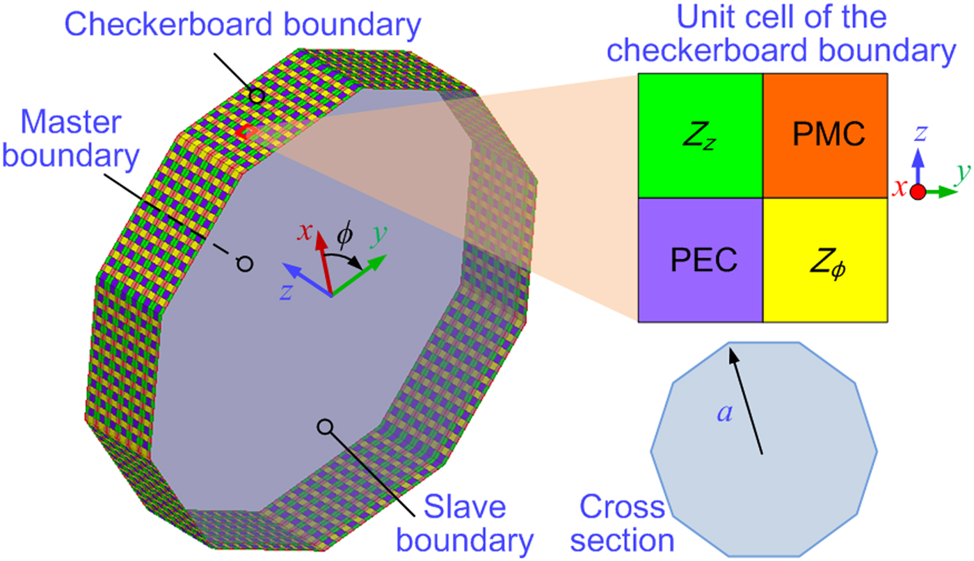
The model is illustrated in Fig. 2. It is a hollow waveguide structure with decagonal cross-section. Ideally, a structure with more side faces is closer to a circular waveguide, which is more helpful in getting accurate results, but it also increases the model complexity. Here the model with ten side faces is proved to be accurate enough. For every side face, the checkerboard structure is utilized to model the anisotropic boundary [Reference Quarfoth and Sievenpiper24]. The checkerboard structure is an array consisting of periodic unit cells. Each unit cell includes four ideal boundaries, which are perfect electric conductor (PEC), perfect magnetic conductor (PMC), and two isotropic impedance boundaries Z ϕ and Z z. The size of the cell is 0.5 mm, much less than the wavelength of our interest, so the effective surface reactance can be obtained by averaging over the cells according to the direction of a considered mode. For the waves propagating in the azimuthal direction, the PEC and Z ϕ boundaries are in series and average to a surface of Z ϕ/2. The PMC and Z ϕ are also in series and average to infinite value since the impedance of PMC is infinity. Using the harmonic mean, an impedance of Z ϕ in the azimuthal direction can be obtained by averaging Z ϕ/2 and infinity in parallel. The same analysis is used for the waves propagating in the axial direction, and gives an impedance of Z z. The boundaries are assumed to be lossless, so only reactance values are set for them. The length of this waveguide is set to be 3 mm, so a lattice of 6 × 10 cells is distributed on each side face. Master and slave boundaries are respectively set on the two ends of the waveguide, and phase delay between them is set. In this way, an equivalent structure with infinite length is solved in the eigenmode solver, and the boundary can be regarded as anisotropic on a macroscopic level with distinct reactances in the azimuthal and axial directions.

Fig. 2. Model in HFSS eigenmode solver. It is a waveguide structure with decagonal cross-section. Each side face distributes the checkerboard boundary that comprises an array of unit cells in subwavelength scale. Each cell consists of four ideal isotropic boundaries, which are PEC, PMC, Z ϕ, and Z z. Two ends of the waveguide are set to be master and slave boundaries.
The cutoff frequencies of the modes, which correspond to the phase delay of zero, with varying surface reactance values are plotted in Fig. 3. The first five modes are analyzed, which are TE11, TE21, TE01, TM01, and TM11 modes. Figure 3(a) shows the cutoffs of the modes when Z ϕ varies from −j400 to j400 Ω and Z z remains zero. Figure 3(b) shows the cutoffs when Z z changes from −j400 to j400 Ω and Z ϕ remains zero. Comparing the cutoff frequencies of these modes predicted by the theoretical equations in the last section and the simulated results, one can easily find that the simulated ones with discrete cutoff values match quite well with the theoretical continuous curves. It is interesting to observe that the curves of TE01 and TM11 modes intersect at the points where Z ϕ = 0 and Z z = 0, implying their same cutoff behaviors as degenerate modes in a normal waveguide with a conducting boundary.

Fig. 3. Cutoff frequencies of the first five modes obtained from eigenmode simulations, in comparison with the theoretical results. The decreasing trends of the cutoff frequencies with increasing reactances are observed. (a) Z ϕ varies from −j400 to j400 Ω, and Z z remains zero. (b) Z z varies from −j400 to j400 Ω, and the other remains zero.
Observing the results, it is clear that the cutoff frequencies decrease with the increasing reactance values. Particularly, when the reactances are negative, the cutoff frequencies are higher than those of a conducting waveguide; when the reactances become larger, the cutoffs drop and become lower than the ones of the normal waveguide. Z ϕ has significant effects on the cutoff properties of the TE modes, but hardly impacts TM modes. On the contrary, Z z strongly affects the TM modes, but barely affects TE modes. To be a control, a similar waveguide with circular cross-section, instead of decagonal, is also simulated in the solver. Its side wall is directly set to be an isotropic boundary, which is permitted in HFSS. Its reactance value is swept, which means the reactance components in the two directions vary simultaneously. It turns out that the cutoffs of the modes change in accordance with their behaviors shown in Fig. 3 with the corresponding reactance values, demonstrating the validation of our modeling methodology. Certain surface modes are also noticed with the increasing reactance terms, but their coupling effects with the considered modes can be negligible, which will be proved by the transmission analysis in the next section.
Changing the reactance value in a specific direction is therefore suggested to be an effective approach to manipulate the cutoffs of the modes, thus to enhance the single-mode bandwidth extension and avoid the mode degeneration for the waveguide. Positive Z ϕ is helpful in reducing the cutoff frequency of the dominant TE11 mode, which was proposed for the bandwidth extension. Now we know that the cutoff frequency of TM01 mode, which is the second lowest mode of the circular waveguide, can be raised by reducing Z z values, so the single-mode bandwidth should be further enlarged. Similarly, the cutoff frequencies of TE01 and TM11 mode can be purposely separated, such that a bandgap can be created where only TE01 mode propagation is supported but the other suppressed.
Driven modal simulations
To demonstrate further the manipulating effect of the anisotropic lining on the cutoffs, transmission performances of the modes are examined through driven modal simulations using HFSS. The model is illustrated in Fig. 4. It is a hollow waveguide with the decagonal cross-section. The checkerboard boundaries with 15 rows of the unit cells are fitted along the axial direction on each side face. Two ends of the waveguide are set as port 1 and 2, respectively. In order to reduce the coupling effect between the boundaries and the ports, two sections set as PEC boundaries are placed between them. During the simulations, port 1 is excited, and transmission coefficients, or S 21, of the modes through the waveguide are calculated.

Fig. 4. Model in HFSS driven modal solver. The checkerboard boundary with 6 × 10 cells are fitted on each side face of the waveguide. Two ends of the waveguide are set as ports 1 and 2. Between the ports and the checkerboard boundaries are PEC. During the simulations, port 1 is excited with the first five modes, and transmission coefficients of the modes are calculated.
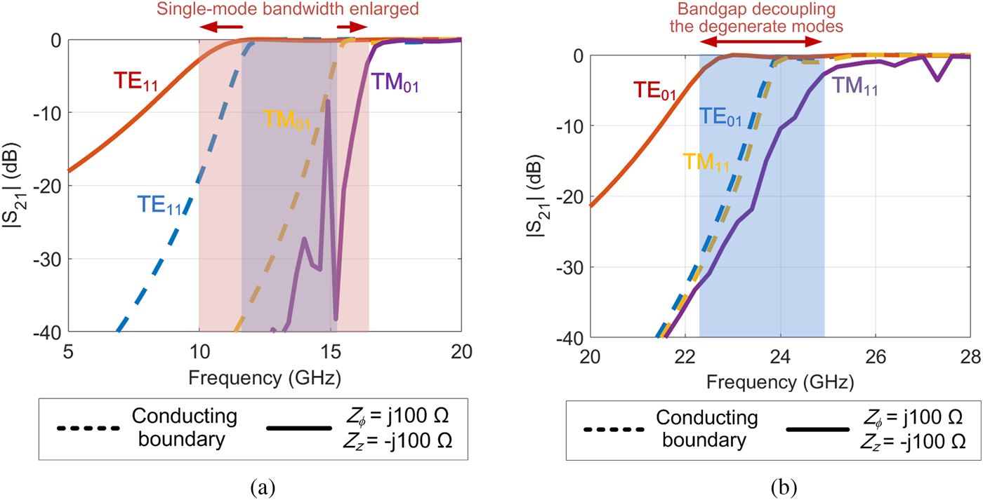
To begin with, the decagonal waveguide is analyzed with conducting boundaries, which are realized by either setting Z ϕ and Z z to be j0.01 Ω, or removing the checkerboard structures and setting the side walls of the waveguide to be PEC directly. The results with the two settings turn out to be exactly the same, which are plotted in Fig. 5 as dashed lines. Observing Fig. 5(a), it is clear that the −3-dB points of TE11 and TM01 modes locate at about 11.5 and 15.1 GHz, respectively, denoting a single-mode bandwidth of 3.6 GHz.

Fig. 5. Simulated magnitudes of the transmission coefficients affected by the anisotropic reactance boundary. (a) TE11 and TM01 modes. Owing to the boundary, the single-mode bandwidth is significantly enlarged. (b) TE01 and TM11 modes. With the boundary settings, the two degenerate modes are decoupled within a noticeable bandgap.
Theoretically, any positive imaginary values assigned to Z ϕ would reduce the cutoff frequency of TE11 mode, and any negative imaginary values given to Z z would raise that of TM01 mode. However, as the reactance values become higher, the EM fields would be confined closer to the boundaries, causing unexpected surface modes. In the simulations here, therefore, Z ϕ and Z z are set to be j100 and −j100 Ω, respectively. The results are shown in Fig. 5(a) as solid curves. It is seen that the −3-dB point of TE11 mode moves downward to about 10 GHz, while that of TM01 mode rises to 16.5 GHz, which means that the bandwidth is enlarged significantly from 3.6 to 6.5 GHz (by 80.5%). The results agree well with the eigenmode simulations and theoretical predictions.
The avoidance of the degenerate TE01 and TM11 modes are demonstrated as we examine the transmission coefficients of the two modes, as depicted in Fig. 5(b). With the conducting boundary, the dashed transmission curves are almost overlapping, since they share the same propagation constant and thus transmission property. With the anisotropic boundary condition, the −3-dB point of TE01 mode decreases from 23.5 to 22.2 GHz, while that of TM11 mode increases to 24.8 GHz. This implies that a frequency gap of 2.6 GHz (9.1%) is created by the anisotropic boundary, within which the waveguide permits TE01 mode but blocks TM11 mode.
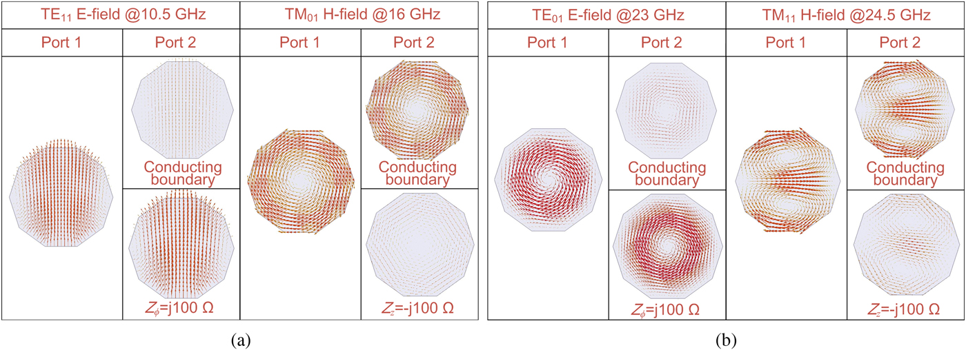
Figure 6 illustrates the field distributions of the modes on ports 1 and 2 at typical frequency points with the reactance boundaries. They look almost the same as the ones in a normal circular waveguide. Reading the E-field distributions of TE11 mode at 10.5 GHz shown in Fig. 6(a), it is seen that its propagation is blocked by the waveguide with PEC boundary, but it is permitted by the reactance boundary with Z ϕ = j100 Ω. This means that its cutoff frequency moves downward across 10.5 GHz because of the boundary. As for TM01 mode, its transmission efficiency at 16 GHz deteriorates when Z z becomes −j100 Ω, implying that its cutoff frequency rises to be higher than 16 GHz. Similar phenomena are also shown in Fig. 6(b), proving that the cutoff frequency of TE01 mode becomes lower than 23 GHz, and the one of TM11 mode increases to be higher than 24.5 GHz. Together with the curves, the manipulating effect of the reactance lining on the cutoffs is convincingly demonstrated.

Fig. 6. Field distributions of the modes on the two ports, showing the changes of transmission efficiency. The mechanism behind the transmission change is the cutoff frequency movement caused by the anisotropic boundary. (a) TE11 and TM01 modes. (b) TE01 and TM11 modes.
Implementation Discussions
In this paper, a lattice of checkerboard structures consisting of ideal isotropic boundary cells are employed to model the anisotropic lining of the circular waveguide. However, the structures are not practical in real designs. So far, a large number of anisotropic metasurfaces have been studied theoretically and experimentally, and led to applications in transmission lines [Reference Gok and Grbic36, Reference Elek, Tierney and Grbic37], waveguides [Reference Quarfoth and Sievenpiper38–Reference Quarfoth and Sievenpiper40], scattering manipulations [Reference Hou, Long, Wang and Sievenpiper41], antennas [Reference Li, Xiao and Sievenpiper17, Reference Fong, Colburn, Ottusch, Visher and Sievenpiper35, Reference Minatti, Faenzi, Martini, Caminita, Vita, González-Ovejero, Sabbadini and Maci42, Reference Selvanayagam and Eleftheriades43], and so on. These artificially engineered surfaces were implemented by periodic arrangement of “meta-atoms,” which are subwavelength-scaled configurations composed of metal textures on dielectric substrates based on the printed-circuit-board (PCB) technique.
Several challenges are required to be considered when a PCB metasurface is utilized as a lining in the circular waveguide. First, the reactance characteristics of the boundaries in this article are assumed to be constant disregarding the frequency. This approximation is promising for the theory validation. But for a real metasurface, the properties are dispersive, so care should be taken to make sure appropriate reactance values occur within the frequency region of interest. It should be noticed that several common-used frequency selective surface elements with inductive terms, such as wire grid, ring slot, and, of course, conducting ground, as well as those with capacitive terms, such as square patch, square loop, and Jerusalem cross, were reviewed in [Reference Li, Xiao and Sievenpiper44]. Specifically, a modified bow-tie-like cell topology was proposed to support TM and TE modes simultaneously within a frequency region, which can be an inspiration for anisotropic linings with positive or negative reactance characteristics. Second, a curved metasurface fit inside a cylindrical geometry may cause unexpected distortion to the impedance properties, which is normally extracted in advance from a planar lattice with infinite cell distributions. Therefore, particular techniques may be needed for an accurate design of a wrapped surface. Third, loss is always believed to be an issue induced by the use of lining, so dielectric materials with low loss tangent are required. In addition, as mentioned above, unwanted surface modes would be inevitably caused by a lining if the reactance values are large, which may deteriorate the transmissions, so proper reactance values should be carefully chosen.
Conclusion
To summarize, we have reported the manipulating effects of the anisotropic reactance linings on the cutoff behaviors of a circular waveguide as well as its potential applications of single-mode bandwidth enhancement and degenerate mode avoidance. Modal derivations are at first presented to predict the cutoff features of the modes. It is found that TE modes are affected by Z ϕ, whereas TM modes are impacted by Z z. When the reactances vary from negative to positive, cutoffs of the modes move from high frequencies, across the ones of a normal conducting waveguide, to lower frequencies. The theoretical results are then validated by the eigenmode simulations using HFSS, where a decagonal waveguide structure with checkerboard boundary settings is utilized for the first time to model the curved anisotropic impedance boundary. This cutoff-controlling mechanism can lead to some potential applications by lowering the cutoff frequencies of TE modes and raising those of TM modes at the same time. As proved by the driven modal simulations, the single-mode bandwidth is obviously broadened, and a band region decoupling the degenerate TE01 and TM11 modes is achieved with proper anisotropic reactance values. It should be noted that at the moment the reactance boundary is ideally frequency independent. With the implementation considerations discussed in this paper, our next steps would be designing curved tensor reactance metasurfaces and their cutoff manipulating investigations on a waveguide prototype in our frequency range of interest.
Acknowledgements
This work was supported in part by the National Natural Science Foundation of China (Grant No. 61801117), in part by the China Postdoctoral Science Foundation (Grant No. 2018M642139) and in part by the Postdoctoral Research Funding of Jiangsu Province (Grant No. 2018K290C). The thoughtful comments from the reviewers are appreciated.
Author ORCIDs
Zhangjie Luo 0000-0003-4866-9187
 Zhangjie Luo received his B.S. degree in electronic and information engineering and his Ph.D. degree in radio physics from Sichuan University, Chengdu, China, in 2008 and 2015, respectively. From 2012 to 2014, he was with the Applied Electromagnetics Group, University of California, San Diego, La Jolla, CA, USA, as a Visiting Ph.D. student. From 2015 to 2017, he was with the Institute of Electronic Engineering, China Academy of Engineering Physics, Mianyang, China, as a Research Staff. Currently he is a post-doctoral fellow with the State Key Laboratory of Millimeter Waves, School of Information Science and Engineering, Southeast University, Nanjing, China. He was one of the finalists for the “Best Paper Award” in ISAP 2018 Busan and an awardee of the “Young Scientist Award” in PIERS 2018 Toyama. His research interests include metasurfaces and antenna technologies.
 Tie Jun Cui received his B.Sc., M.Sc., and Ph.D. degrees in electrical engineering from Xidian University, Xi'an, China, in 1987, 1990, and 1993, respectively. In 1993, he joined Xidian University, and was promoted to an Associate Professor in November 1993. From 1995 to 1997 he was a Research Fellow with the Institut fur Hochstfrequenztechnik und Elektronik (IHE) at the University of Karlsruhe, Germany. In 1997, he joined the Center for Computational Electromagnetics, Department of Electrical and Computer Engineering, University of Illinois at Urbana-Champaign, as a Postdoctoral Research Associate and later worked as a Research Scientist. In 2001, he became a Cheung-Kong Professor in the Department of Radio Engineering, Southeast University, Nanjing, China. He has published over 400 peer-review journal papers in Science, PNAS, Nature Communications, Physical Review Letters, Advanced Materials, etc., which have been cited more than 18 000 times (H-factor 69). His research interests include metamaterials, computational electromagnetic, etc.
 Hui Feng Ma received his B.S. degree in electronic engineering from the Nanjing University of Science and Technology, Nanjing, China, in 2004, and his Ph.D. degree from the State Key Laboratory of Millimeter Waves, Southeast University, Nanjing, China, in 2010. In 2010, he joined the School of Information Science and Engineering, Southeast University, Nanjing, China, and was promoted to Associate Professor in 2011 and to full Professor in 2015. His current research interests include metamaterial antennas, spoof surface plasmon polaritons, and other novel metamaterial functional devices including theoretical design and experimental realization. Dr. Ma was a recipient of the Second Prize of National Award for Natural Science, China, in 2014, and the First Prize of Natural Science from the Ministry of Education, China, in 2011. His research of 3-D ground carpet cloak realized by using metamaterials has been selected as one of the “10 Breakthroughs of Chinese Science in 2010.”