


I. INTRODUCTION
Carbon nanotubes (CNTs) [Reference Dragoman1, Reference Ijima2] are made of grapheme-rolled sheets. CNTs can either be multi-walled (MWCNTs) or single walled (SWCNTs). The small-diameter CNTs have a 2/3 semiconductor behaviur, whereas those with a large diameter always have a metallic behavior. MWCNTs with an outer diameter greater than 25 nm have radio frequency (RF) metallic properties at high frequencies (≥40 GHz) [Reference Jun3] and can support high current densities of about 108 A/cm2. The MWCNTs also have exceptional physical properties: an electrical conductivity of 7.78 × 10⁴ S/m [Reference Grimes4], a high elasticity, and high thermal conductivity ranging from 20 to 400 GPa [Reference Poncharal5] and from 1800 to 3000 W/m K [Reference Kim6], respectively. There are three different switch geometries using CNTs: the cantilever, the bridge, and the tweezer geometry [Reference Jang7]. In this paper, PECVD (plasma-enhanced chemical vapor deposition) is used to make carbone nanotubes at a middle-range temperature of about 600–800°C.
II. DESIGN, MODELING, AND CHARACTERIZATION OF NEMS
A) NEMS design
The goal of our work was to perform two NEMS structures in tweezer configuration, one with an ohmic contact and another with a capacitive contact. The ohmic-contact switch uses a metal–metal contact (Fig. 1(a)), whereas the capacitive-contact switch uses a metal–dielectric contact (Fig. 1(b)). The NEMS switching is realized in two steps. During the first step, a low potential (<1 V) is applied between the two MWCNTs. Then a high DC polarization is applied on one or both pull-in electrodes (Fig. 1). One pull-in electrode and its nearest MWCNT have the same electrostatic charging (positive or negative) and hence contribute to the NEMS switching. This method allows us to minimize the potential V 1 and to transport higher current through the contact without any damage for the device.

Fig. 1. NEMS switches using ohmic contact (a) and using capacitive contact (b).
We also report on the realization of a capacitive NEMS based on MWCNT coated with a SiO2 dielectric layer, a first building block for further RF filter realization.
B) NEMS theoretical considerations
The MWCNT motion in an NEMS switch is defined by [Reference Dequesnes8]
where W is the MWCNT motion, E the Young's modulus, I the inertia moment, F elec the applied electrostatic force, F vdW the van der Waals force attraction between atoms, and F elast the elastic force of MWCNT.
The electrostatic force is defined by [Reference Dequesnes8]

where V is the pull-in voltage between the MWCNTs (F elec + F elast = 0), ɛ 0 the vacuum permittivity, L the length of the MWCNT, R the outer diameter of MWCNT, and r the distance between the MWCNTs.
In the tweezer configuration, the elastic force is defined by [Reference Dequesnes8]
with

where D ext and D int are, respectively, the outer and inner diameter of the CNTs.
The van der Waals interaction between close MWCNTs is given by the relation [Reference Dequesnes8]
where ρ 1 and ρ 2 are the volume densities of the two materials in contact (ρ CNT = 1.4 g/cm3) [Reference Rols9], C 6 the attraction between two atoms (C CNT = 15.2 eV Å6) [Reference Dequesnes8], and L C the contact length when the MWCNTs are pulled in. The van der Waals force must be estimated when the NEMS switch is pulled in. The dimensions of this component are defined in order to have F elast/F vdW >1.
C) MWCNTs growth by PECVD
The preferred method for synthesizing vertically aligned CNTs is dc plasma-enhanced chemical vapour deposition (dc-PECVD), using transition metal catalyst films/particles to seed and sustain the growth [Reference Melechko10, Reference Cojocaru11]. The plasma can be operated in the diode mode or in the triode mode, the latter bringing more flexibility to the process. The growth temperature typically ranges from 600 to 750°C depending on plasma chemistry.
In triode configuration, during the process, a plasma is created between two electrodes and an electric field is applied between the plasma region and the substrate (negatively polarized) (Fig. 2(a)). Using this configuration, we have developed [Reference Cojocaru12] a water vapor-assisted growth process where H2O is employed (instead of NH3 generally used) for the purpose of etching excess a-C during growth. This new process yields very long tubes and the growth rate shows no sign of saturation, even after long plasma exposure times. Figure 3 shows an example of localized growth, obtained from Ni pads (~1 µm in diameter), using a classical optical lithography aligner. For this particular experiment, we have used a mixture of C2H2 and H2O at a temperature of 650°C. CNTs over 10 µm long can be observed, corresponding to a 90-min growth time. Another advantage of this new H2O-based process is that the growth temperature can be lowered (down to 500°C) without inducing a significant degradation of the CNT's crystalline quality.

Fig. 2. Schematic (a) and SEM picture (b) of PECVD growth.

Fig. 3. MWCNTs growth by PECVD (C2H2 + H2O) on TiN/Ni dots of 1 µm diameter.
D) NEMS fabrication
The NEMS design requires CNTs growth on metallic electrodes (Fig. 1) which must support the growth temperatures from 600 to 800°C. The tweezer NEMS switch realized by Jang et al. [Reference Jang7] have been made on niobium at 600°C. Optimized PECVD growth conditions require in particular a growth temperature of about 700°C. This implies the use of a metal with a higher electric conductivity than niobium at growth temperature. Figure 4 shows some metals that have a greater melting temperature and a higher electric conductivity than niobium.

Fig. 4. Melting temperatures in °C (a) and electric conductivities in S/m (b) [Reference Kittel13], for different bulk transition metals.
Molybdenum has two main advantages: firstly, Fig. 4(b) shows that it has the best electric conduction with tungsten, and secondly, it is deposited by evaporation allowing a better alignment of successive technology levels. Javey et al. [Reference Javey14] have already used the molybdenum grown by PECVD at 800°C.
The fabrication process is summarized in Fig. 5 where all technology levels allowing NEMS realization are shown. By using both equations (2) and (3), we obtained a voltage of 13 V on the pull-in electrode. Figures 6(a) and 6(b) show the NEMS switching when a voltage of about 14 V is applied on the pull-in electrode (V electrode) with a bias of 0.01 V between the nanotubes commuted. Figure 6(c) shows an increase of current for a pull-in voltage on the electrode of 14 V leading to a corresponding increase of current from 0 A to 4 nA. This behavior is characteristic of a pull-in between two conductive elements and confirms our theoretical result of 13 V on the pull-in electrode. After the switching, the nanotube length has decreased by 200 nm, proving the contact and the nanotube fragility to current crossing between two nanotubes in contact.
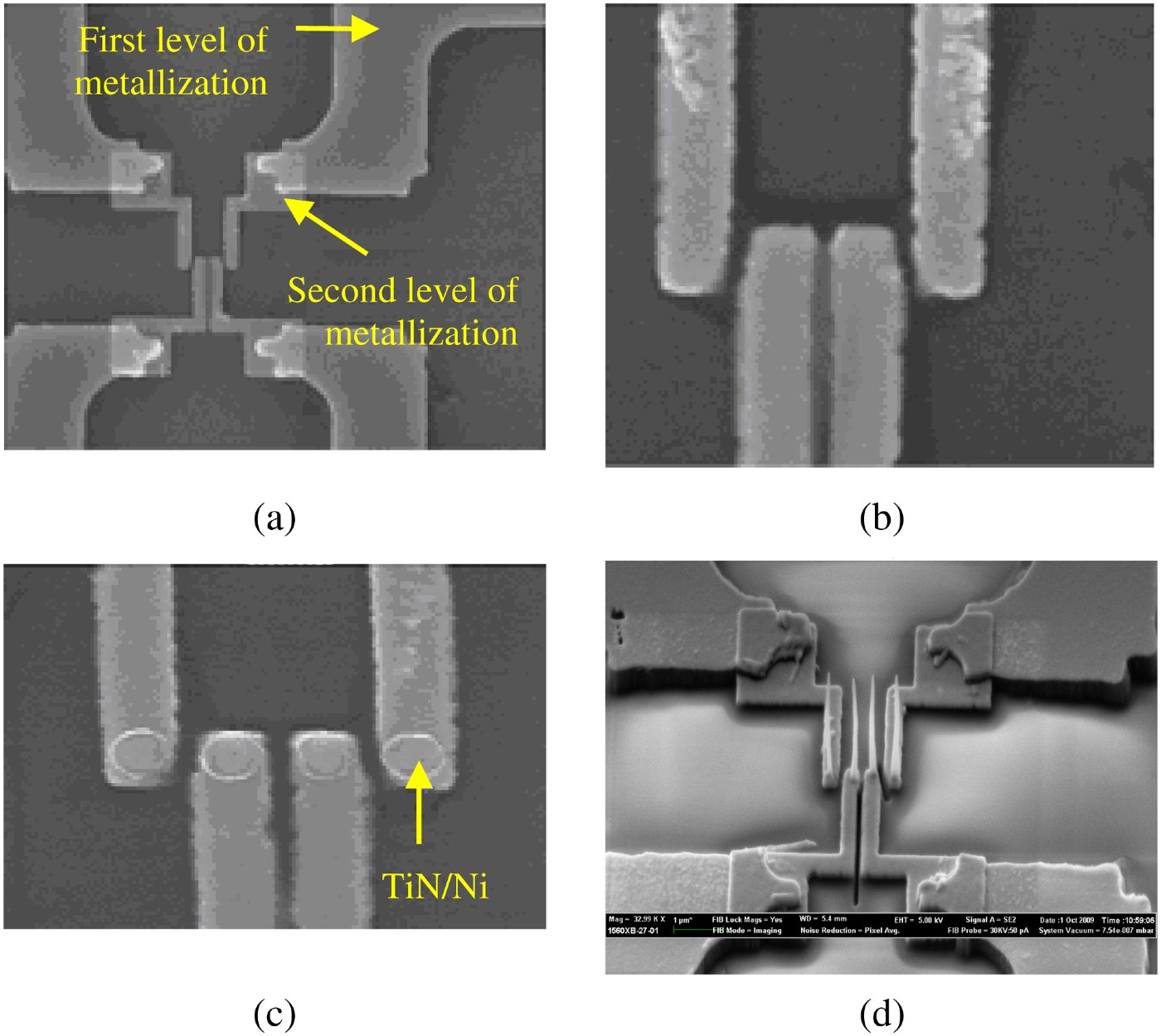
Fig. 5. (a) SEM pictures of the first metallization level (Mo) realized by optic lithography and (b) second metallization level by electronic lithography (e-beam) with nanobeam LTD (c) SEM pictures of TiN/Ni dots after sputtering and evaporation depositions realized by e-beam. (d) SEM picture after the MWCNTs growth at 700°C.
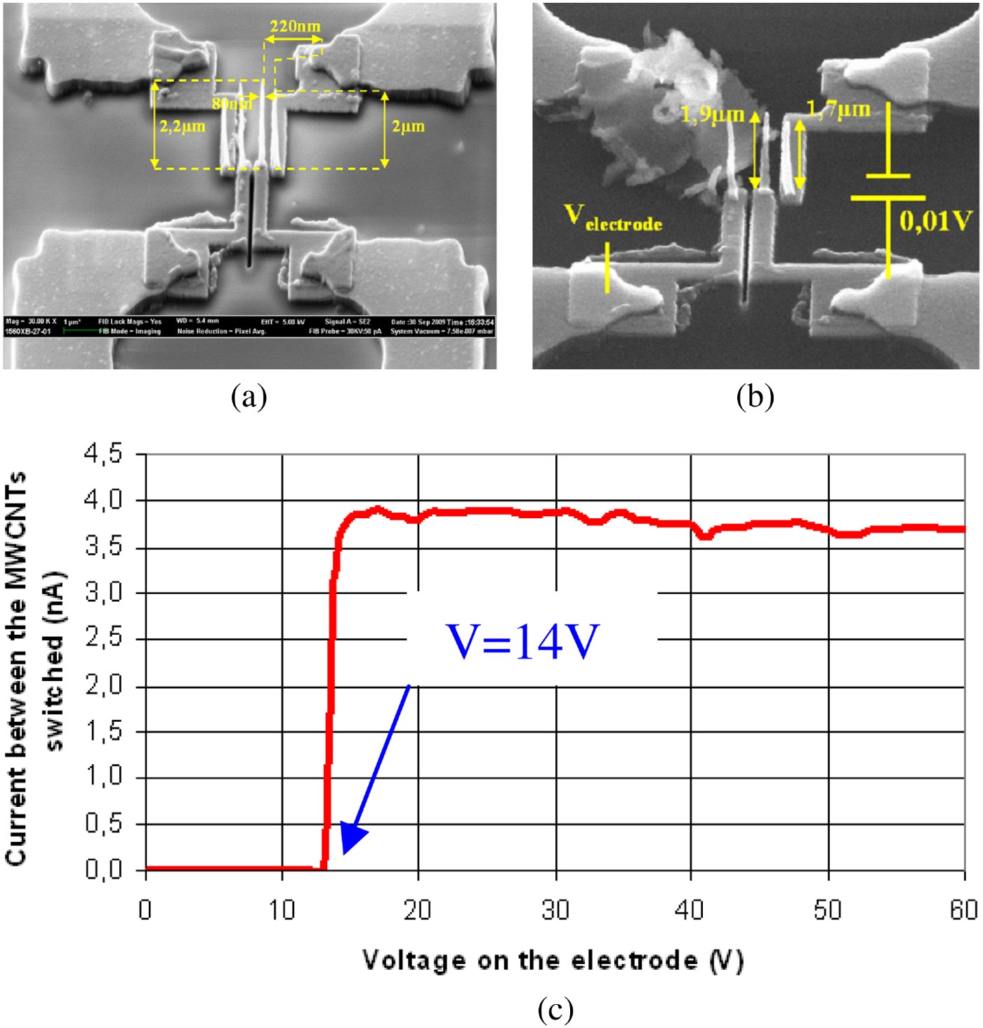
Fig. 6. SEM pictures of NEMS before (a) and after(b) pull-in voltage. Current dependence on voltage (c).
E) Towards capacitive NEMS
To design the capacitive NEMS switch (Fig. 1b), a MWCNT has to be coated with a dielectric SiO2 layer. The coating method (electron beam induced deposition (EBID)) is realized using the focused ion beam). Diaceto-di-tert-butxysilane is injected near the MWCNT, molecules of which are broken by the gallium ion flux (Fig. 7), owing SiO2 to be locally deposited.
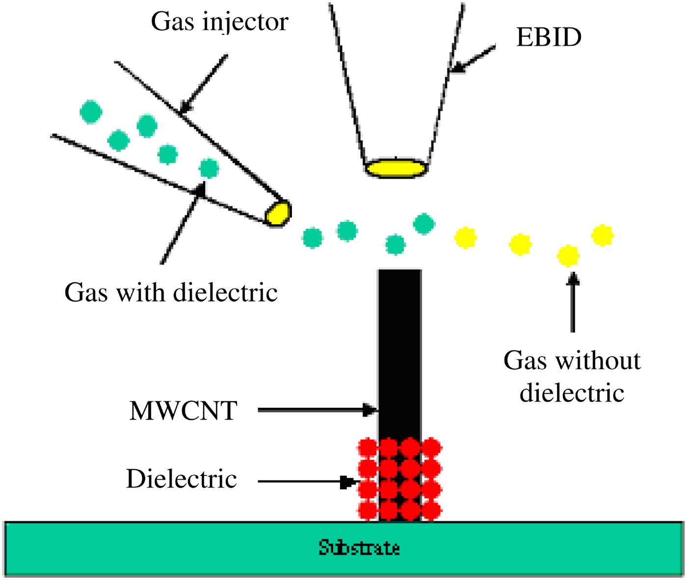
Fig. 7. Schematic of the EBID method.
Figure 8 shows the SiO2 deposition around the MWCNT resulting in an increase in both its diameter and length. With this method, a metallization layer (platinum, tungsten, etc.) can also be deposited to improve the ohmic contact.
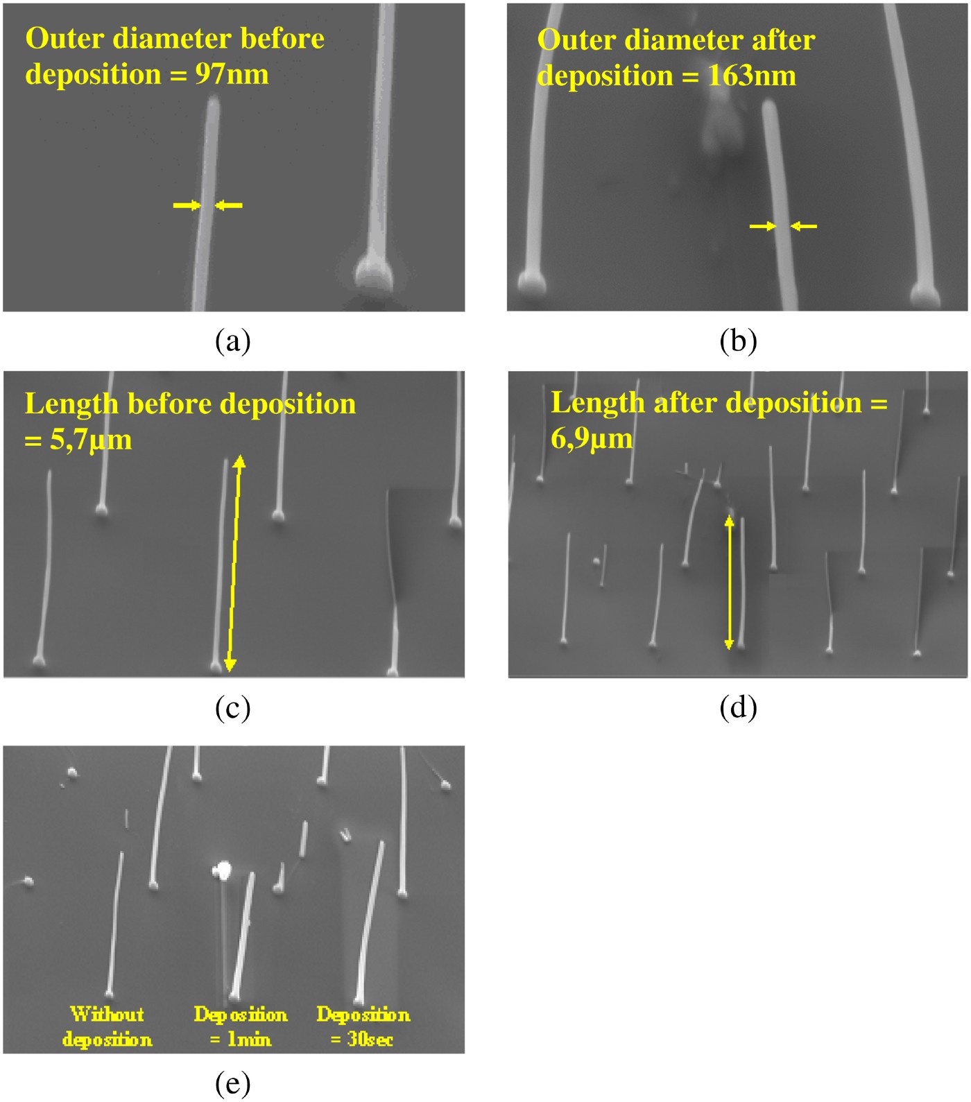
Fig. 8. SEM pictures of MWCNT before SiO2 deposition (a and c) and after SiO2 deposition during 3 min by EBID (b and d). (e) SEM comparison of three MWCNT diameters, without deposition and after deposition (30 s and 1 min).
III. RF SIMULATION RESULTS
Hyper-frequency simulations have been realized with the RF simulation software HFSS developed by Ansoft on a parallel RF NEMS design (Fig. 9(a)) and a molybdenum metallization. The MWCNT frequency data [Reference Jun3] and the molybdenum metallization give the possibility to define the coplanar wave guide dimensions. At frequencies equal to or higher than 40 GHz, the molybdenum skin thickness is 600 nm [Reference von Hippel15]. In order to obtain a 50 Ω adaptation, the line width and the distance between the signal line and the ground lines are 36 and 27 µm, respectively. Figure 9(b) shows the design of one switch; the more they are drawn up in parallel, the better are the RF results. Figures 9(c) and 9(d) show RF NEMS in the on and off states, respectively.
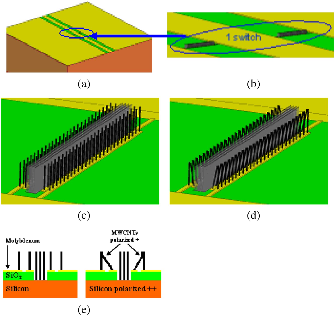
Fig. 9. Design of RF parallel NEMS (a); blow-up of one switch (b); ohmic contact: on state (c), off state (d); schematic view of the RF switch polarization (e).
The switching is realized by high DC polarization of the substrate which also polarized the CNT forest (Fig. 9(e)). Thus, the substrate is used as a pull-in electrode.
Figure 10 shows the first RF simulation results from a metal–metal contact. With insertion losses lower than 2 dB at 50 GHz (Fig. 10(b)) from eight switches at the “on” state, and isolation higher than 7 dB (Fig. 10(d)) from eight switches, this ohmic RF NEMS design allows future applications. Figure 10(e) also presents one encouraging data with the insertion losses (“on” state) on isolation (“off” state) ratio in percent. This graphic shows at 50 GHz a ratio of 26% from eight switches.

Fig. 10. Insertion losses of ohmic RF-NEMS (a) and capacitive RF-MEMS (b) switches in the ON state; isolation of ohmic RF-NEMS (c) and capacitive RF-MEMS (d) switches in the OFF state; IL/I ratio of the NEMS (e).
Figure 11 shows the capacitive RF NEMS in the on state (Fig. 11(a)) and in the off state (Fig. 11(b)), with the MWCNTs on the molybdenum ground coated with a SiO2 dielectric layer. As for the ohmic RF NEMS, the switching is realized by high DC polarization of the substrate which also polarized the CNT forest (Fig. 11(e)).

Fig. 11. On state for a capacitive contact (a) and off state for a capacitive contact (b).
Figure 12 shows the results of RF simulations from a metal–dielectric contact. With 50 GHz insertion losses lower than 1.5 dB (Fig. 12(b)) from eight switches in the on state, and an isolation higher than 8 dB (Fig. 12(d)) from eight switches, such a capacitive RF NEMS design is promising for future applications just like the insertion losses on-state on isolation (off-state) ratio of 17% at 50 GHz for eight switches (Fig. 12(e)).

Fig. 12. Adaptation (a) and insertion losses of capacitive RF NEMS switch in the “on” state (b); reflection (c) and isolation of capacitive RF NEMS switch in the “off” state (d); insertion losses on isolation ratio in % units (e).
IV. CONCLUSION
The NEMS fabrication success using vertically MWCNTs gives a pull-in voltage of 14 V close to the simulation value of 13 V. The material deposition by EBID makes possible the capacitive NEMS fabrication. The simulation results of ohmic RF NEMS and capacitive RF NEMS allows one to consider their fabrication for specific applications in the near future.
 Afshin Ziaei received the B.S. degree in Electronics Engineering from the University of Paris XI (Orsay) in 1997 and the M.S. degree in Electronics and Microwaves Engineering from the University of Paris VI (Jussieu) in 1998 and he received Ph.D. degree in microwave from the Department of Electronics Engineering at CNRS-IEMN (Institut d'Electronique et de Microélectronique et de Nanotechnologie) in 2001. He joined the research engineer at Thales Research & Technology, France, in 1999. His research interests include the development, design, fabrication, and characterization of RF MEMS (Micro Electro Mechanical Systems) components such as mechanical switches, transmission lines, etc. He was involved or in charge of many French or European Projects (such as ARHMS (coordinator of project), ARESSAT, MEMS2, PEA MEMS, FLAME). He is a member of IEEE. Role in the project: (coordinator of project).
 Michaël Charles received the M.S. degree in Electronics and Microwaves Engineering from the University of Paris-Est Marne-la-Vallée in 2006 and he received Ph.D. degree in microwave from the Department of Electronics Engineering at CNRS-IEMN (Institut d'Electronique et de Microélectronique et de Nanotechnologie) in 2010. He joined the research engineer at LNE (Laboratoire National de métrologie et d'Essais) for the microwave department, France, in 2010. His research interests include the maintains of the RF power standards.
 Matthieu Le Baillif received the B.S. degree in Electronics Engineering from the University of Lille I in 2003 and the M.S. degree in Electronics and Microwaves Engineering from the University of Limoges (XLIM) in 2005. He joined the research engineer at Thales Research & Technology, France, in 2005. His research interests include the development, design, fabrication, and characterization of RF MEMS (Micro Electro Mechanical Systems) and other RF components such as mechanical switches, transmission lines, etc.
 Stéphane Xavier received his Master in thin layer and surface engineering from the University Louis Pasteur de Strasbourg (France) in 2005. He then pursued his scientific career with a Research and Technological Diploma from the University d'Evry-Val-d'Essonne (France) in 2007. He joined Thales Research & Technology in 2007 and his specialist field has been cold cathodes based on carbon nanotubes for field emission and microwave tubes applications. Currently in the Technological and Submicronic Process Lab, he is responsible of the electron-beam lithography equipment and the associated research development. Over the past 4 years, he has been heavily involved in several european and national projects (Spiders, Copernicus, Technotubes, Sims, Gospel, Opther… .)
 Amaël Caillard is a permanent research fellow at the Centre National de la Recherche Scientifique (CNRS, French research Centre) in Orléans from 2009. He received a M.S. degree in electronics and optics from the University of Orléans in 2003 and he received a PhD in plasma physics from the University of Orléans in 2006 and from the Australian National University in 2007. He joined the laboratory « Laboratoire de Physique des Interfaces et Couches Minces » at the Ecole polytechnique in 2008 as a postdoctoral fellow for one year. His research interests include the development of low pressure plasma techniques for preparing new designs of fuel cell electrode, Li-Ion batteries electrode and microelectronics and optoelectronics based on carbon nanotubes. Over the past 3 years, he has been involved in several european and national projects.
 Cojocaru Costel Sorin (1974) received his physics engineer degree from the University of Bucharest, Romania, in 1996. From 1996 to 2001 he joined as assistant researcher the National Institute for Laser, Plasma and Radiation Physics (Bucharest), Romania. He received his PhD degree in Physics from the University Louis Pasteur (Strasbourg), France in 2003. He joined CNRS in 2005 at LPICM-Ecole Polytechnique where he is presently leader of the NanoMaDe-NanoMaterials and Devices Group. Since 1996 his research area focuses on the nanostructured materials synthesis and nanotechnologies. He is presently involved in carbon nanotubes, graphene and semiconductor nanowires synthesis and collective organisation for advanced electronics and novel devices (energy storage/harvesting, CNTs/NWs based FETs, gas/biological sensors, NEMS, field emission devices…).


