I. INTRODUCTION
The continuous growth of the demand for broadband high-capacity communications and services has recently increased the interest for the possible exploitation new frequency bands. As far as satellite telecommunications are concerned, the Q/V band (35–75 GHz) represents an inviting free spectrum resource beyond the widely used Ka band [Reference Aloisio, Angeletti, Coromina and De Gaudenzi1–Reference Rossi3]. This frequency band is suitable for the development of broadband satellite communication systems that would provide high-capacity services, as, for example, broadband multimedia, interactive internet protocol (IP) applications, and Television multicasting [Reference Aloisio, Angeletti, Coromina and De Gaudenzi1–Reference Rossi3]. This type of systems would be able to provide such services also to remote rural locations or mobile users, as ships, aircrafts, and trains. Another possible application for Q/V band telecom satellites are secure communications between space platforms [Reference Aloisio, Angeletti, Coromina and De Gaudenzi1]. In addition to offering a wider available bandwidth, compared to the lower frequency bands, the use of Q/V spectrum has also the advantage of enabling the generation of smaller satellite beams for a given fixed antenna aperture, and of implementing user terminals with reduced dimensions [4]. Clearly the development of Q/V band telecommunication satellite systems demands for highly integrated space-qualified microwave circuits microwave monolithic integrated circuit (MMICs) for the implementation of the communication front-ends. As a confirmation of this growing interest, the implementation of Q/V band MMICs is also a target included in the priority activities of the Advanced Research in Telecommunications Systems program (ARTES 5.1 [4]) of the European Space Agency, which is a long-term initiative funded to support innovative concepts and technologies for satellite telecommunications. In this context, this paper describes the design, implementation, and characterization of an MMIC frequency converter circuit for Q-band satellite communications. This circuit was developed in the framework of an industrial research program dedicated to small-medium enterprises, funded by the Italian Space Agency (ASI), named SALINT – “Development of High Integrated MMIC for Satellite Telecommunication Antennas in Ka and Q/V Bands”.
II. TECHNOLOGY
The technology selected for the design is the space-qualified PH25 process from the European foundry United Monolithic Semiconductor. This process is based on a 0.25 µm gate-width GaAs/InGaAs/AlGaAs pHEMT technology, featuring a T-shape aluminum gate obtained by double electron-beam lithography. The final thickness of the wafer is 100 µm. Typical field effect transistor (FET) characteristics are: V TH = −0.75 V, I dss = 340 mA/mm (measured at V ds = 2.5 V), g m = 500 mS/mm (measured at V ds = 2.5 V, V gs = 0 V), 7 V breakdown voltage. The transistors' cut-off frequency is 90 GHz. The transistors can be used for power amplification, with typical power density of 250 mW/mm, or for low-noise applications, with minimum NF = 0.6 dB at 10 GHz, NF = 0.9 dB at 20 GHz, and NF = 2 dB at 40 GHz. Diode components are available in the process for mixer and detector applications. Schottky diodes are obtained from the pHEMT structure by short-circuiting source and drain terminals. These devices are designed for low junction capacitance and low series resistance, thus obtaining a cut-off frequency as high as 330 GHz. The process offers two metal interconnect layers and a complete set of passive components: 330 pF/mm2 silicon nitride metal-insulator-metal (MIM) capacitors, spiral inductors, via holes, air bridges, metal, and GaAs resistors.
III. MMIC MIXER DESCRIPTION AND DESIGN
The circuit was designed exploiting active and passive device models provided in the foundry design kit. Both electrical linear and nonlinear (harmonic balance) simulations and electromagnetic (EM) simulations were employed in the design. Electrical simulations were performed using Agilent ADS software, whereas Sonnet EM suite was exploited for EM simulations, which were fundamental for the design of the passive balun structures.
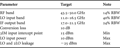
The main target specifications for the design are shown in Table 1 and were identified with the support of the ASI and Thales Alenia Space Italy. These specifications set the choices for the mixer type and topology:
(1) Subharmonic operation was chosen to enable the use of an X-Ku band LO.
(2) An LO buffer was included to minimize the LO power requirements.
(3) A double-balanced structure was needed to maximize the port-to-port isolations and also for the unfeasibility to use a single-balanced structure with the same balun for LO and RF frequencies, since they are largely spaced due to the subharmonic operation. It is worth noticing that, due to the subharmonic operation, the diodes' conductances at 2LO are all in phase, thus the circuit does not have all the same balancing properties of a fundamentally pumped double-balanced mixer [Reference Maas5], even though its operation still ensures a 2LO leakage within the specification limits (Table 1), as shown with the characterization measurement in Section IV.
(4) Unbiased diode mixer is practically the only possible choice to implement a compact double-balanced structure with the necessary symmetry [Reference Maas5]. Indeed, other possible balanced active solutions (e.g. Cold FET, transconductance mixer, Gilbert cell) would require complex topologies (also for the distribution of bias lines), which are ineffective in terms of performance (due to parasitic effects and spurious couplings) and space occupation at such high frequency, using this type of technology.
Table 1. Main target specifications.

RBW, relative bandwidth.
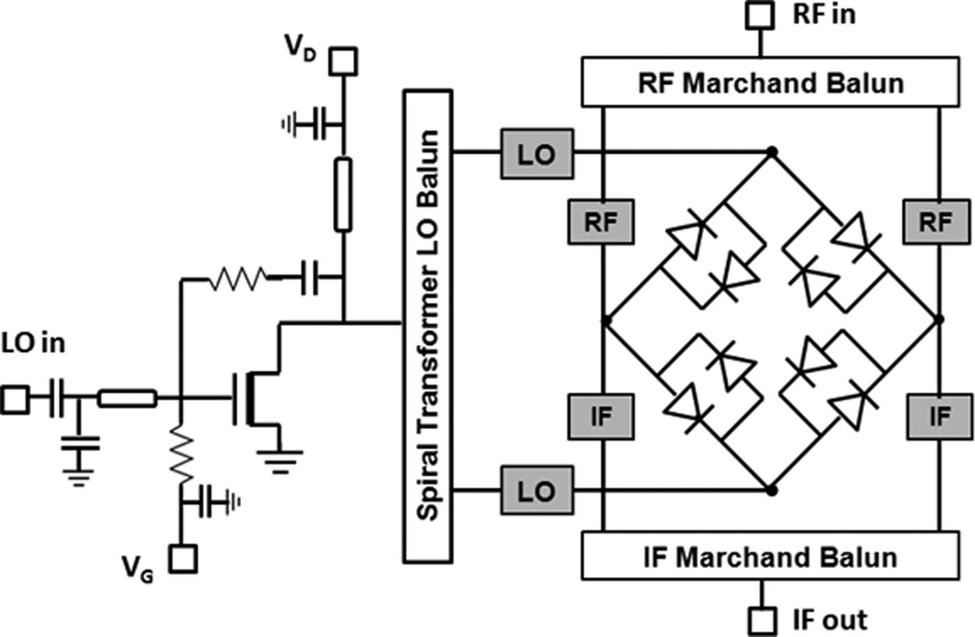
The functional schematic of the circuit is displayed in Fig. 1. The core of the mixer is composed of four antipodal diode pairs in a ring structure. Antipodal diode pairs are used to obtain the desired subharmonic operation, since due to symmetry, the large-signal conductance of the pair has a first harmonic contribution at twice the pumping LO frequency [Reference Maas5]. In Fig. 2, the detailed layout of the eight diodes implementing the mixer nonlinear core is shown: two air bridges (in the upper part of the layout) are used for the crossovers of the LO connections with RF and IF lines, whereas other two bridges (bottom part) are inserted to maintain the symmetry of the structure. Owing to the high application frequency, the layout of the diodes' connections was kept as compact as possible and accurately simulated (EM simulations) to take into account in the design any possible spurious couplings which may cause asymmetric behavior. Also the airbridge crossovers of the LO balun branches with the IF/RF balun feed lines (see Fig. 2) have been accurately EM simulated: even though the two crossover structures are clearly asymmetric (see Fig. 2), the coupling between microstrip lines is so weak (<−45 dB) that none appreciable effects were found on simulated circuit performance.
Fig. 1. Functional schematic of the circuit.
Fig. 2. Layout of the mixer core.
The diode choice is a compromise between different constraints: conversion loss, linearity (p1 dB, IP3), and LO power requirements. Indeed transconductance, parasitic capacitive effects, and power handling capability vary with the diode active area; moreover, diode impedances also vary with dimensions and introduce another compromise with matching network losses and bandwidth. Considering these trade-offs, 4 × 6 µm diodes were selected for the ring mixer design.
The LO buffer amplifier was designed exploiting a 6 × 75 µm pHEMT in common source configuration, with a drain to gate Resistor-capacitor (RC) feedback network for extending the bandwidth. The buffer operates in class A and is dimensioned to provide the power level needed to properly pump the eight diodes (four antipodal pairs) of the ring, when operating in linear condition with V D = 2.8 V and I D = 80 mA.
The RF and IF balancing structures are implemented as traditional coupled-lines Marchand baluns, whereas the LO balun is synthesized exploiting a bifilar planar transformer-lumped structure, similar to the one in [Reference Huang, Chen and Horng6], since a λ/4 distributed structure was too large at the LO frequency. In Fig. 3, the layout of the LO balun is shown. The two bifilar windings are implemented by means of 5 µm width microstrips with 5 µm spacing: the length of each winding is λ/4 at the LO central bandwidth; the second end of input microstrip is terminated with an open circuit, whereas the output (coupled) microstrips are terminated at one end with a via hole to ground (the other two ends being the balun-balanced outputs). Each winding is formed by 4.5 turns. Even-mode and odd-mode impedances of the baluns were synthesized to optimize their balancing and matching performance. Distributed microstrip networks are used to match the balun impedances to the diodes at the different frequencies (see picture of the MMIC in Fig. 6). Air bridges allow the overcrossing between different matching networks necessary to access the diodes' ring.
Fig. 3. Layout of LO balun: bifilar planar transformer.
Devices' operative currents and voltages were monitored to ensure their operation with a proper derating with respect to maximum safe levels, which is compulsory for high reliability space applications. Particular attention was devoted to the operative junction temperature (T j) and maximum DC forward current (I g). Simulated values of T j = 110°C and I g = 0.5 mA per diode finger were well below the process's maximum ratings of T j = 175°C and I g = 1 mA/finger, respectively.
IV. CHARACTERIZATION MEASUREMENT
In addition to the overall MMIC, also some cut-outs of circuit subsections were inserted in the foundry run in order to test the accuracy of the design. As an example in Fig. 4 (on the left-hand side) the picture of the cut-out of the LO balun is shown: ground-signal-ground (GSG) pads are included in the structure to access the balun with microwave probes for its measurement. The same structure is simulated with a three-dimensional planar EM simulator (right-hand part of Fig. 4). In Fig. 5, the measured performance of the balun is shown along with a comparison with the simulated data. Within the application bandwidth (11–16.5 GHz) the phase error stays below 6° and the amplitude error is <0.5 dB. The maximum insertion loss is 1.8 dB and the input return loss (RL) is better than 12 dB. The fitting between simulations and measurements is very good, considering the frequency and the complexity of the structure.
Fig. 4. Left: picture of the cut-out of the LO balun. Right: three-dimensional view of the LO balun for EM simulations.
Fig. 5. Comparison between simulations and measurements of the LO balun (port 3 is the Balun input port). Measured phase error is below 6°, amplitude unbalance below 0.5 dB and insertion loss 1.8 dB maximum in the application frequency band 11–16.5 GHz.
The MMIC was mounted in a test jig (Fig. 6) for its characterization: the MMIC accesses at RF, LO, and IF are connected to external GSG probes on alumina substrate by means of 100 µm width wide gold ribbons, that are necessary for the circuit integration in the front-end module and were taken into account in the design. Ribbons are preferred to bonding wires since they are clearly less inductive at such high frequencies.
Fig. 6. Picture of the actual MMIC (2.33 × 2.33 mm2) and picture of the measurement test jig with GSG accesses including ribbons.
Measured RLs at the three mixer ports with the LO frequency fixed at 13 GHz are shown in Fig. 7 along with the simulations data. Matching performances are quite good and fairly similar to simulations.
Fig. 7. MMIC port matching for LO frequency at 13 GHz: measured and simulated data.
Measured and simulated MMIC conversion gain with fixed LO and variable RF is shown as a function of IF frequency in Fig. 8 with a comparison with simulations: small differences within 1 dB are observed between the measured and simulated data. In Fig. 9, different measurements at three fixed IF (selected at the IF bandwidth edges and center) while sweeping RF and LO frequencies along the entire specification bandwidth are shown: the conversion loss stays between 8 and 12 dB for all the possible frequency conversion plans.
Fig. 8. Measured and simulated MMIC conversion gain with fixed LO and variable RF.
Fig. 9. Measured and simulated MMIC conversion gain with fixed IF and varying the RF and LO frequencies across the entire application bandwidth.
Also the linearity performances of the circuit were characterized. A minimum input referred P1 dB = 2 dBm was measured for every mixer conversion plan; as an example, in Fig. 10 measured data of the mixer nonlinear conversion gain with LO = 13.25 GHz are shown. The IP3 test was performed with two tones with 0.5 MHz frequency spacing, whose power was varied between −30 and 1 dBm (see Fig. 11): the LO frequency was kept fixed at 13.25 and 14.5 GHz, while the tones' central frequency was swept over the RF bandwidth. In those conditions, a minimum input IP3 = 15 dBm was measured, as shown in Figs 11 and 12 for the two different frequency plans.
Fig. 10. Measured gain compression of the MMIC mixer.
Fig. 11. Measured IF fundamental and intermodulation mixer products of the two-tone linearity test with LO = 13.25 GHz, RF = 43.5 ± 0.25 GHz, and IF = 17 ± 0.25 GHz.
Fig. 12. Measured input IP3 of the MMIC mixer.
The LO and 2 × LO leakage at the IF port were measured for all the possible operative conditions: as can be seen in Fig. 13, these power levels are always below −25 and −35 dBm, respectively. Since the incident LO power at the diode ring is PLO = 16 dBm, the isolation given by the subharmonic balanced mixer structure is about 41 and 51 dB for LO and 2LO, respectively: this high level of suppression is also an indication of the good performances of the IF Marchand balun (the LO performances were already separately proved with the dedicated measurements on the cut-out shown in Fig. 5).
Fig. 13. Measured MMIC LO and 2LO leakage with PLO = 10 dBm.
Finally also both in-band and out-of-band spurious have been measured in the IF frequency band (15–25) GHz, with LO frequency at 15 GHz. Both types of spurious are below −67 dBc, when the input RF signal power is at −26 dBm, which is satisfactory for the application.
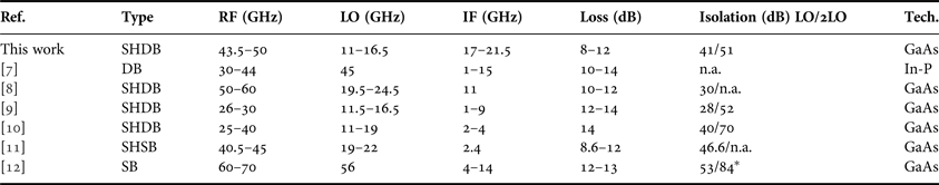
A comparison with similar products in the literature is not an easy task due to the quite peculiar frequency conversion plan from Q to Ku-K band (usually lower IF bands are exploited). For the same reason, similar commercial off the shelf products are not available for a comparison. Nonetheless in Table 2 a benchmark with published circuits, which have some similarities with the proposed mixer, is presented. The conversion loss obtained by the proposed mixer can be certainly considered at the state of the art for MMIC diode mixers at similar frequencies.
Table 2. Comparison with similar mixers.
SH, subharmonic; DB, double balanced; SB, single balanced.
*Simulated results.
Also the obtained LO and 2LO isolation of 41 and 51 dB, respectively, are within the best performance obtained by similar products in Table 2. By analyzing the layout of the circuits proposed in Table 2, it is interesting to note that different choices are made for the topology of the balun structures: balun solutions exploiting λ/4 line structures (Marchand balun [Reference Yu, Walden, Schmitz and Lui7], Lange coupler + λ/4 line [Reference Zelley, Barnes and Ashcroft8], and Rat-Race balun [Reference Florian, Scappaviva, Feudale, Monaco and Filicori12]) occupy more chip space, but tend to ensure slightly more isolation properties compared to bifilar planar transformer baluns, which clearly minimize space occupation [Reference Lai, Lin, Chang, Lin and Wang9, Reference Blount and Trantanella10]. These very compact structures should be the choice for both RF and LO balun when space saving is the primary target [Reference Lai, Lin, Chang, Lin and Wang9, Reference Blount and Trantanella10]. Another possible solution exploited in [Reference Chiou, Lian and Yang11] with excellent isolation results is the use of reduced-size Marchand baluns, whose dimensions are decreased due to the use of lumped-element capacitive loading [Reference Guo, Zhang, Ong and Chia13].
V. CONCLUSION
An MMIC doubly balanced subharmonic diode ring mixer was designed exploiting a European space-qualified GaAs pHEMT Technology. The mixer performs the down-conversions from Q (43.5–50 GHz) to Ku-K band (17–21.5 GHz) exploiting a (11–16.5 GHz) LO signal, due to subharmonic operation. The mixer core is a ring structure of eight diodes in antipodal pairs configuration for subharmonic operation. A single-stage LO buffer using a pHEMT in common source configuration with an RC feedback network is also integrated in the chip. Lumped and distributed microstrip-based balun structures and matching networks at the three ports of the circuit enable to obtain very good suppressions of LO harmonics and spurious products at the IF output port. The extensive use of EM simulations and a detailed nonlinear design allowed to be compliant with the target specifications with a single foundry run.
ACKNOWLEDGEMENTS
This work was supported by the Italian Space Agency (ASI) under the contract – SALINT – “Development of High Integrated MMIC for Satellite Telecommunication Antennas in Ka and Q/V Bands”, contract number I/030/11/0. The authors from MEC would like to thank Andrea Suriani and Francesco Vitulli from Thales Alenia Space Italy for their support in the definition of the MMIC specifications.
Davide Resca was born in Bologna, Italy, in 1979. He is currently a Senior Microwave Design Engineer at MEC srl, Bologna (Italy). He joined MEC in January, 2009, as a MMIC designer after his Ph.D. and post doc studies with the Department of Electronics, Computer Science and Systems (DEIS) of the University of Bologna. He is responsible for MMIC design, hybrid module design, passive and active device characterization, and modeling. His current research interests are advanced CAD techniques for microwave-integrated circuit design, EM sub-circuit advanced modeling, and planar filter design synthesis and analysis.
Rafael Cignani was born in Ravenna, Italy, in 1975. He received the Laurea degree in Telecommunications Engineering from the University of Bologna, Bologna, Italy, in 2000 and the Ph.D. degree in Information Engineering from the University of Ferrara, Ferrara, Italy, in 2004. During his doctoral studies, he collaborated with the Department of Electronics, Computer Science and Systems (DEIS), University of Bologna. He is currently a Graduated Technician with the Department of Electrical, Electronic, and Information Engineering (DEI), University of Bologna. His research activity is mainly oriented to MMIC design and nonlinear circuit modeling and design techniques.
Corrado Florian (S'02–M'04) was born in Forlì, Italy, in 1975. He received the M.S. degree in Electronic Engineering from the University of Ferrara, Ferrara, Italy, in 2000 and the Ph.D. degree in Electronic and Computer Science Engineering from the University of Bologna, Bologna, Italy, in 2004. He is currently a Research Associate with the Department of Electrical, Electronic, and Information Engineering (DEI), University of Bologna. During his academic career, he has been a Lecturer of the Electronics for Communications and Power Electronics. His main research activity is in the areas of microwave monolithic circuit design, hybrid RF circuit design, nonlinear dynamic system characterization and modeling, microwave, and millimeter-wave device characterization and modeling.
Andrea Biondi was born in Italy in 1982. He received the Laurea degree in Electronic Engineering from the University of Bologna, Bologna, Italy, in 2009. In 2009, he joined the MMIC research group of the Department of Electronics, Computer Science, and Systems (DEIS) of the University of Bologna, as a Research Assistant. Since 2011 he has been employed by MEC srl, Bologna, Italy, as the RF designer with his activities mainly oriented to hybrid and monolithic microwave-integrated circuit design and characterization. His main research interests are in the field of RF power amplifiers and microwave circuits for space applications and communication systems.
Francesco Scappaviva was born in Italy in 1978. He received the Laurea degree in Electronic Engineering and the Ph.D. degree in Electronic Engineering from the University of Bologna, Bologna, Italy, in 2004 and 2009, respectively. In 2004, he joined academic spin-off MEC – Microwave Electronics for Communication, Bologna, Italy, as the RF Research Engineer with his activities mainly oriented to hybrid and monolithic microwave-integrated circuit design and characterization. In the same company, where he is currently working, in 2009 he was appointed Technical Manager and in 2012 he became a member of the Board of Directors. His main research interests are in the field of RF power amplifiers and microwave circuits for space applications and communication systems. Since 2010 he is involved in the managing of Industrial and Research programs.