I. INTRODUCTION
RF-MEMS technology is considered to be one of the most promising solutions for advanced frequency agile RF architectures. Combining this technology with the impressive performances of BiCMOS's in a single process represents a switching paradigm in RF systems design. Even though process dispersions in CMOS technology are known to be very small, they may yield significant deviation in the behavior of MEMS devices. Therefore, it is very important to study the relationship between the fabrication process parameters and the effects of the variation on RF performance, which allow the Design for Reliability implementation. An accurate and versatile model would significantly help to predict the process variation effects in design level.
In terms of reliability, all of the failure mechanisms have already been studied and classified by means of the Failure Mode and Effect Analysis (FMEA) [Reference De Wolf1, Reference Lucyszyn2]. Literature has shown different design solutions in order to implement Design for Reliability in RF-MEMS. For example, the use of carbon nano tubes (CNT) [Reference Bordas3], UNCD [Reference Goldsmith4], and proximity switches [Reference Goldsmith5] in order to avoid dielectric charging. Also, the use of hard materials such as ruthenium [Reference Feixiang6] has improved the resistive switches lifetime. Finally, in commercial applications, the design of Built-In Self-Test (BIST) circuits [Reference Nguyen7] in order to compensate for degradation during the lifetime has been presented as a very effective solution for co-integrated MEMS-CMOS processes.
In order to implement BIST circuits to enhance lifetime, standard methodology and failure criteria definition are missing nowadays in the community. One of the key issues is to detect after manufacturing which parameter of the device (electrical or mechanical) can be used as an indicator of possible future failure mechanisms in each specific application. This could eliminate the default switch due to infant mortality over the wafer defining the yield of the process regarding reliability. This is the purpose of the present work developed in the framework of aerospace application.
II. DESCRIPTION
A) Brief technology description
Figure 1 illustrates the RF-MEMS switch integration in IHP's 0.25 µm SiGe BiCMOS process (SG25H1) based on five aluminum metal layers [Reference Kaynak8]. The capacitive switch is built between the two metal layers (M2 and M3). M3 is the membrane and it is realized by using a stress controlled Ti/TiN/AlCu/Ti/TiN stack. The RF line is built in M2 and the high-voltage electrodes are formed by using the bottom metal layer (M1). The additional RF-MEMS switch process only adds one more mask to the standard BiCMOS flow in order to release the RF-MEMS device. Thus, it does not increase the mask cost significantly (while the full BiCMOS process costs about 1k€, the additional mask costs 700€), which is one of the main concerns of these technologies.

Fig. 1. Switch (top) and cross-section (bottom) with a zoom of the contact region of the BiCMOS-MEMS fabrication process.
All of the fabricated devices use the same movable part (thus contact region) [Reference Kaynak9] and the target operating frequency is tuned by adding series inductances at the anchors of the switch [Reference Kaynak10] creating different versions of the switch. The main advantage of this solution is that the membrane is mechanically optimized only once in order to yield high reliability, while different switches can be designed to work at different frequencies without affecting the mechanical performance. On the other hand, the bandwidth (BW) of the switch is reduced at lower frequencies because of the higher values of the inductances (hence higher losses and lower Q-factor) that are needed. For this reason, these switches are typically suitable for applications at frequencies higher than 40 GHz.
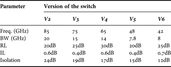
As an example, Table 1 shows the measured RF performance (RL, IL, and Isolation) of five versions of the shunt switch at the working frequency (Freq). The BW is established at ±20% of the maximum isolation. As described before, the movable part is the same in all of the versions, only the inductors are added at each anchor (out of the etched area) keeping the same mechanical properties in all of the versions.
Table 1. RF Performance of de-embedded switches.
Although the pull-in occurs around 37 V, 40 V actuation voltage is applied in order to ensure a stable contact of the membrane in down position and hence a stable value of the isolation at the working frequency.
III. LUMPED-ELEMENTS-BASED MODEL
A scalable lumped-elements model is proposed for the different switches presented in [Reference Torres Matabosch11]. The importance of the proposed model is that all of the the lumped-elements are associated to a constitutive part (shape and size) of the device, which provides a complete and detailed electrical description. This allows it to trace back and to detect possible manufacturing flow or deviation due to technological dispersion. In addition, it provides information about the quality of the fabricated devices since it can be directly correlated to the performance of the device.
In Fig. 2, the model of the switch is presented with the values of the associated elements. This equivalent circuit is based on two parallel resonant circuits. The main resonance which determines the working frequency is due to the down state capacitance and the inductors in the arms of the switch (Z MEMS and L anchor). The secondary resonance is associated to the capacitance between the membrane and the electrodes, and the inductance of the bias lines (C M1–M3 and L electrode). In both cases, an additional series resistor is added in order to compute the losses of the inductors (R anchor and R electrode). The inductor L anchor is modeled using a pi-network as proposed in [Reference Dickson12]. The UP/DOWN capacitance ratio is suitable for phase shifting applications, for example.
Fig. 2. Lumped-elements based model of the switch with the substrate coupling network (red) and the model of the transmission line (black). Z MEMS is the contact zone model in UP and DOWN states.
The transmission line is an RLCG model combined with a substrate coupling network well-known in the BiCMOS process modeling. The reason for using this approach is due to its simplicity in being used in network simulators (Spice) and the substrate losses already known can be easily added. The values of each parameter of the substrate coupling network (C ox2, C ox1, R subs, and C subs) are deduced from the process specifications as in (1) where C Mi-subs is the coupling from Metal i (M1 or M2) to substrate per μm2 (defined by the process), A line is the surface of the line, C subs is measured and σ Si is the resistivity of the substrate. R, L, and C are deduced from the standard modeling of CPW [Reference Simons13].
 $$\eqalign{C_{oxi}& =A_{line} \cdot C_{Mi - subs}\comma \; \quad i=1\comma \; 2\comma \; \cr R_{subs}& =\displaystyle{{\varepsilon _r \varepsilon _0 \sigma _{Si} } \over {C_{subs} }}=405\; \Omega\comma \; \cr \varepsilon _r& =11.9\quad C_{subs}=170fF\comma \; \quad \sigma _{Si}=0.5\, \Omega {\rm m}.}$$
In Fig. 3, the measured RF performance of all of the presented switches (V2–V6) is compared with the model adapted with its corresponding L anchor value. The measurement results were taken over an 8-inch wafer for more than 50 samples; therefore, it also shows the dispersion of the RF performance over the wafer. These results show very good agreement between the model and the measurements within the entire frequency band (30–110 GHz). The difference between the model and the measurement is due to the model of the substrate, which is not adapted in the entire band but it can be considered that at the working frequency the equivalent circuit agrees with the measurements
Fig. 3. Measured RF performance (colored) and model (black): V2 (red), V3 (blue), V4 (pink), V5 (cyan), and V6 (purple).
A) Fabrication process deviations characterization
Owing to the nm-range thickness variations and the non-uniform deposition of the metals, the stress gradient of the suspended membrane varies over the wafer changing the distance between the metals (~4%) which yields significant variation (5–6%) on the MEMS capacitance (C MEMS) in both states. The same stress variation also affects directly the membrane to actuator capacitance (C M1–M3) which turns out to be responsible for the device BW. It is therefore apparent that the understanding of these two capacitances, and their variation, enables the direct monitoring of the device RF behavior.
In order to verify the relationship between RF deviation and C MEMS variation, LF measurements (at 1 MHz) using an impedance analyzer (Agilent 4294A Precision) of the UP and DOWN state capacitance (C MEMS) are conducted. The parasite capacitances of the substrate and C MIM are de-embedded by means of specific test structures (identical devices without the bridge part). These measurements show a Gaussian distribution from the mean value in both states (Fig. 4 (top)). By applying the computed deviations to the lumped-elements circuit model shown above, the effect of the fabrication tolerances can be reproduced in the entire band. A Monte Carlo analysis of the model with 50 trials is performed and compared with the measurements of the 50 devices under test showing very good agreement (Fig. 4 (bottom)).
Fig. 4. Deviation in LF measurements of C MEMS in UP (C UP_dev) and DOWN (C DOWN_dev) state (top) and comparison between measured (red) and model (gray) RF performance with the computed fabrication process deviations.
It is noteworthy is that the relation between, C M1–M3 and the RF performance can only be established by using the equivalent circuit since this capacitance cannot be measured experimentally. In fact, in order to be measured it would need extra test structures to de-embed the coupling effects with other metal layers. These extra structures and additional measurements would hamper real time monitoring. For this reason, a rough first estimation of C M1–M3 is extracted from the model by exploiting the parallel plate capacitance formula followed by more accurate identification based on curve fitting of the isolation around the secondary resonance.
B) Versatility of the proposed model
It has already been seen in the previous section that when the designer changes the working frequency (increasing or decreasing the inductance of the anchors), the proposed model can easily describe it. This section demonstrates that the model can be used to carry out the design of a new component based on the same technology.
The series switch is conceived by modifying the metal layer interconnection layout of the V4 switch (48 GHz). The membrane is disconnected from the ground in order to connect it to the output Fig. 5.
Fig. 5. Cross-section of the shunt (left) and series (right) switch used for the experiment.
The model of the series switch is presented in Fig. 6. In comparison with the shunt model, only a new transmission line is added in order to consider the connection of the inductances to the anchors. To alleviate this effect and improve the isolation, a shunt inductor is added.
Fig. 6. Layout (left) and adapted model (right) of the series switch.
With respect to the shunt version introduced in Section 2 this new design differs for two main parts: (1) The transmission line that connects the membrane with the output (TL1); and (2) the inductor (L shunt) that resonates with CUP and yields better isolation at the desired frequency (40 GHz). For both of the components the same modeling method presented in the previous section is used.
The comparison between the model and the measurements of the series switch is shown in Fig. 7. The series switch present 1.7 dB of IL and 13 dB of isolation at the working frequency (45 GHz) and the model fits well with the measurements in the whole band. The disagreement comes to the lower Q-factor of the parallel inductances. This result proves the versatility of the model allowing the design of new components just by modifying the equivalent circuit and translating the changes in the layout. This is possible thanks to the accurate RF modeling of each constitutive element of the structure including the MEMS part.
Fig. 7. Comparison of RF performance between measurements (red) and model (black).
IV. RELIABILITY OF THE DEVICE
From the manufacturer's point of view, the availability of an effective screening procedure is paramount. The definition of the selection criteria depend on the capability of the component to satisfy the targeted application performance, for the given working conditions. This paper uses the industrial requirements for the space application presented in [Reference Vendier14] by Thales Alenia Space. According to them, a maximum deviation of 10% in V PIN and V POUT and an increase of 1 dB in IL for 1 h of continuous stress are assumed as the failure threshold criteria. The actuation profile has been monitored through the S 12(V) measurements since the DOWN state (contact) position is reached below the mechanical pull-in.
The 8-inch wafer is divided into cells within which the switches are replicated (Fig. 8) (96 switches per cell). From each cell only three devices have been selected for the reliability analysis assuming that the manufacturer ensures uniformity inside the cell (coming from the BiCMOS process). One quarter of the wafer is used for the presented results since horizontal and vertical symmetry applies. The availability of a large number of devices allows a fair monitoring of the process dispersion and it is instrumental to assess the reliability of the device for given industrial specifications. Another important point is that the reliability study presented hereafter can be extended to any type of switches using the same movable part.
Fig. 8. Quarter of 8-inch wafer studied for the reliability tests.
A) Definition of selection criterion
Preliminary tests using the same protocol determined that the V POUT and V PIN could be indicators of failure [Reference Torres Matabosch15]. Afterwards, devices having the best and worst performance over the wafer were selected in order to prove the hypothesis. Three devices (30, 40, and 50 G) of each cell have been held in DOWN position (40 V) during 1 h measuring the IL and the pull-in/out voltage every 10 min. Figure 9 plots the deviation after stress of the pull-out voltage for several identical devices (15) with different initial V POUT. The difference between the devices remains in fabrication process deviations since the etching time is not the same in the entire wafer as will be demonstrated in Section IV-B.
Fig. 9. Relation between the deviation after 1 h of stress and the initial V POUT. The size of the disk (numerically specified) represents the difference between V PIN and V POUT. The black point represents the devices that succeeded the tests.
It is demonstrated that the higher the V POUT, the lower is the deviation after stress. Moreover, the difference between V PIN and V POUT plays also an important role and it should be also as low as possible. Applying the aforementioned industrial requirements (10% deviation in V POUT) on devices taken on the entire wafer, very few devices succeeded the tests. These devices (in black in Fig. 9) have a V POUT > 36 V and |V PIN− V POUT| ≤ 1, which correspond to the selection criteria.
An important remark is that |V PIN− V POUT| should be as low as possible but the measurements show 1 V of difference since setup resolution is 1 V when performing S 12(V).
The condition (|V PIN− V POUT| ≤ 1) is due to the short distance between the different metal layers used for the electrodes and the transmission line. It is well known that the relationship between the gap (g) and the applied voltage (V) is related to the stiffness (k), the initial gap between actuator and membrane (g 0), and the size of the actuator (surface (S), thickness (t d), and material (ε d)) by mean of the following relation (2) [Reference Rebeiz16]:
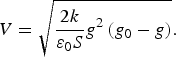 $$V = \sqrt {\displaystyle{{2k} \over {\varepsilon _0 S}}g^2 \left({g_0 - g} \right)} .$$
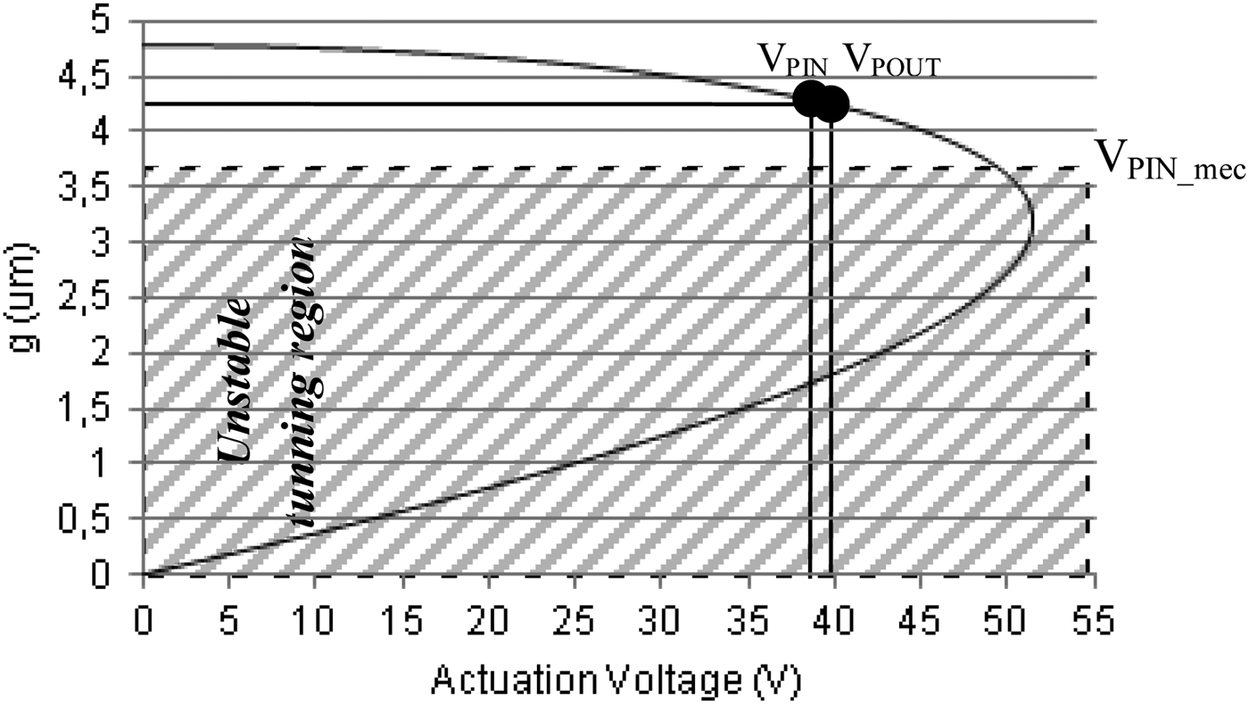
Plotting the g(V) curve of the successfully tested devices (Fig. 10) using (2) (g 0 = 4.8 µm, k = 4.56, S = 80 × 80 µm2), it becomes evident that the correspondent actuation voltage is placed in the quasi-linear region (below mechanical pull-in V PIN_mec) meaning that the V PIN and V POUT are very similar. The distance between membrane and line is smaller than one-third of the distance between the membrane and the electrode (g 0).
Fig. 10. g(V) of a succeeded device showing the computed pull-in and -out voltage and the mechanical pull-in
The monitoring of the performance during the test has shown that the failure occurs during the first 30 min. For this reason, it is concluded that infant mortality is the reason of failure and it is important to predict which devices will suffer from this defect.
It must be pointed out that the values indicated above as V POUT and V PIN do not correspond to actual pull-in and pull-out occurrence. They rather represent the value of potential voltage, at which, the mechanical contact of the membrane with the underneath signal line is achieved. Now, since this contact is obtained far below the pull-in of the actuator (the actual electrostatic driving force is on the lateral electrodes), these two values should be coincident in a well-functioning device. If this is not the case, this deviation can be used to detect a failure mechanism likely associated to the membrane actuation
B) Failure mechanism study
Once the selection criterion has been established, the next step is to develop a technique in order to predict which devices have V POUT > 36 V. The proposed screening protocol is based on distance measurement between different metal layers. This approach is cost-effective (very quick), non-intrusive (no activation of the device is needed) and can be implemented over the whole wafer (also in TCV – Technology Characterization Vehicles specific cells).
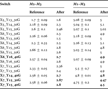
In Table 2 the measurements of the gap between membrane and electrode (M1–M3) and between membrane and line (M2–M3) for the tested devices in UP state (OFF) are depicted and compared with the reference including the dispersion over the same cell. This result demonstrates the possibility to detect with profilometer measurements weather the device is compliant with the targeted performances. Distances about 2.8 and 4.7 µm from M2–M3 and M1–M3, respectively, coincide with pull-out voltages above 36 V which is one of the established criteria.
Table 2. Distance between metals before and after stress.
The name of the switch is given by: Xx_Yy_fG where x,y are the position over the wafer and f is the working frequency.
Comparing both distances (M1–M3 and M2–M3) with the reference value extracted from the devices of the same cell, it has been observed that the failure mechanism is due to fatigue and creep. Since the electrostatic force is applied on the lateral part of the membrane, the creep effect turns out to decrease the distance M1–M3, which implies an increase of the distance between M2 and M3 (Fig. 11). Owing to the design of the device the dielectric charging cannot occur. In the contact area, no difference of electrical potential is applied between the membrane and the line. The electrodes are not covered with dielectric.
Fig. 11. Schema of the mechanical deformation before (black) and after (red) stress.
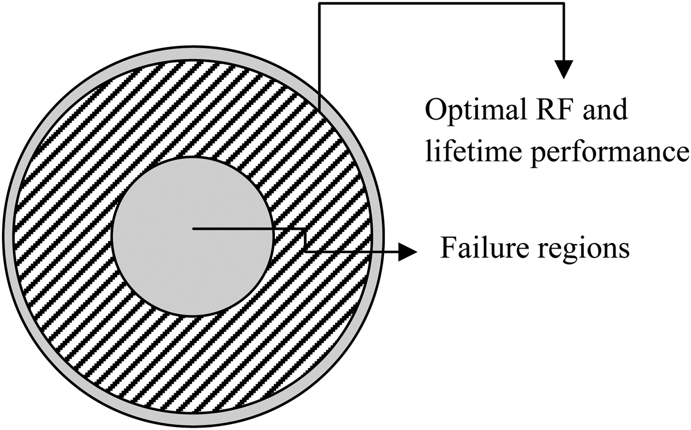
Regarding the distribution over the wafer, it is observed that the regions placed at the exterior part of the wafer succeed the tests (Fig. 12). The reason of this result is that the etching of the cavity is not uniform in the whole wafer reaching the optimal etching time in the region highlighted in Fig. 12 as was confirmed by the IHP. The difference of the needed etching time between regions is due to the different thickness of SiO2 over the wafer coming from the dispersion of the CMOS process. More accurate etching techniques are currently under development to increase the optimal area. Figure 12 represents only indicatively the region where the good compromise of etching rate over the wafer is achieved. This result is very useful for the manufacturer since it allows a performance-based (RF and lifetime) monitoring and analysis of the wafer yield.
Fig. 12. Area of the wafer with optimal RF and lifetime performance.
The occurrence of fatigue phenomena was also observed by comparing the S-parameters in UP state before and after the test (Fig. 13). By using the equivalent circuit model of the device described in Section III, the undesired resonance found at 35 GHz has been properly modeled and attributed to the likely breaking of one of the suspending arms. A clear evidence of this failure mechanism is given by the excellent agreement between the measurement of the defective device (after stress) and the equivalent circuit model modified in order to accounts for this failure (broken arm). This fracture was observed in four devices while the others presented a decrease of M1–M3 and M2–M3 distance described by the model with an increase of the C MEMS and C M1–M3 values.
Fig. 13. Comparison of IL before (black) and after (red) stress with the model (triangle).
With respect to the schematic of Fig. 2, beside the effect of the broken arm on the L anchor, the parameters that have been also modified are the capacitances C MEMS and CM1–M3. In fact, due to the fatigue, the distance between the metals has decreased and both values of capacitance should be modified using (3) and (4), respectively.
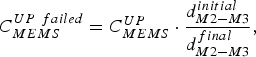 $$C_{MEMS}^{UP\ failed}=C_{MEMS}^{UP} \cdot \displaystyle{{d_{M2 - M3}^{initial} } \over {d_{M2 - M3}^{final} }}\comma$$
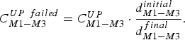 $$C_{M1 - M3}^{UP\ failed}=C_{M1 - M3}^{UP} \cdot \displaystyle{{d_{M1 - M3}^{initial} } \over {d_{M1 - M3}^{final} }}.$$
In order to avoid failure mechanisms associated with fatigue and creep three possible approaches are typically envisioned. Going in order of growing implementation difficulties they are: to increase the effective Young's modulus by material engineering, to increase the membrane thickness and finally to redesign the membrane (anchors) shape. An optimal solution may pass through a combination of them.
V. CONCLUSION
This paper has showed a versatile wide band lumped-elements model for capacitive RF-MEMS switches based on a 0.25 µm BiCMOS process. The excellent agreement between the model and the measurements of five different switches shows that the geometrical variations are accurately taken into account and predicted in the design phase. This flexibility and versatility of the model is demonstrated by proposing a series switch obtained from a model based synthesis and exploiting a rerouting of the metal layer of the same technology. The proposed model can significantly enhance the final performance of the device in design/simulation phase and is very promising for fast optimization of MEMS-based circuits. Finally, this paper has proposed a quick and non-intrusive reliability monitoring technique such to predict creep and/or fatigue induced phenomena and avoid the infant mortality. The method is based on the identification of the indicators of future failures and their optimal values (V POUT > 36 V and |V PIN− V POUT| ≤ 1). The proposed reliability approach has demonstrated its validity and effectiveness in observing and analyzing the MEMS process yield, be it within the same wafer or wafer to wafer. This is a very important achievement for future commercialization of RF-MEMS devices and circuits.
ACKNOWLEDGMENT
The authors would like to thank the IHP pilot line and Christian Wipf for the technical support during manufacturing and RF measurement, respectively, and the partial financial and technical support provided by Thales Alenia Space in Toulouse.
 Dr. Núria Torres Matabosch born in Cerdanyola del Vallès in 1985. She received an engineering degree in Telecomunications from the Polytechnic University of Catalonia in 2009 and received her Ph.D. degree in Micro and NanoSystems 2013 by Université Paul Sabatier – Toulouse III collaborating with the MINC group in LAAS-CNRS. Her main research interests are design and optimization of RF-MEMS devices and reconfigurable circuits towards its commercialization. She has collaborated in the organization ofthe International RF-MEMS Summer School in Toulouse and published more than ten conference papers and four international journals. Since May 2013 she has been with the Radio Navigation Group in Airbus (EADS).
Dr. Fabio Coccetti received the Laurea (MS) degree in Electrical Engineering from the University of Perugia, Perugia, Italy and the Ph.D. title in High Frequency Engineering at the Lehrstuhl für Hochfrequenztechnik at the Technische Universität München (TUM) in Munich Germany, in 1999 and 2004, respectively. In 2000, he spent 7 months, as visiting scientist, at the Radiation Laboratory at the University of Michigan USA. Since September 2004 he has worked as research scientist at the Laboratoire d'Analyse et d'Architectures des Systèmes at the Centre National de la Recherche Scientifique (LAAS-CNRS) in Toulouse, France. During this period he has led numerous research projects going from design and modeling to theoretical and experimental investigation of topics such as power handling and reliability RF Micro and Nanosystems. Dr. Coccetti has been the coordinator of the FP6 projects (European Network of Excellence on RF-MEMS and RF Microsystems – AMICOM NoE) and is currently serving as reviewer of the FP7-ICT projects. In 2008 he joined the company Novamems (Fialab from 2013) as RF-MEMS specialist and R and D project manager. Dr. Coccetti's research interests include numerical techniques optimization, multiphysics (concurrent electrical and thermomechanical), design and modeling of reconfigurable circuits for microwave and millimeter applications, and reliability assessment of RF-MEMS components. Dr. Coccetti has been guest editor of the Transaction on Microwave Theory and Technique and of the International Journal of Microwave and Wireless Technologies. He is currently serving as reviewer of several journals and letters (IEEE-MTT, -TED, -EDL -MWCL, IJMWT, JMEMS, etc.) and he is a member of the technical program committees of international events (IMS, EuMW, ESREF, and Memswave). Dr. Coccetti is a member of the IEEE society and the European Microwave Association (EUMA). Since January 2009 he has been vice-chair of the IEEE MTT-S TC-25 on RF-Nanotechnology and cofounder of the Topical Group on RF-Microsystem Technology within the European Microwave Association (EUMA).
 Jean-Louis Cazaux was born in 1960. He got a Ph.D. in Physics and Electronics in Toulouse in 1985, and then was Post-Doc research fellow at the University of Michigan, Ann Arbor, USA in the field of advanced transistors and circuits for microwave electronics. In December 2003, he obtained a Habilitation (for Researches Steering) from Université Paul Sabatier, Toulouse. He joined Alcatel Space in 1988 as MMIC (Microwave Monolithic Integrated Circuit) designer. From 1996 to 2012, he was the head of the Microwave Advanced Studies within the Microwave Department of what is now Thales Alenia Space. Since January 2013, he has acted as Technology Manager for the Competence Center Electronics of Thales Alenia Space – France. He represents Thales Alenia Space at the EuRAMIG (European Microwave Interested Group) meetings. He represents EUROSPACE, on behalf of Thales Alenia Space, at the SCSB (Space Component Steering Board) and at the Plenary CTB (Component Technology Board) two bodies of the ECSS (European Space Components Coordination) led by the European and National Space Agencies. In 2006, he founded AXIS, a Research Joint Lab between his company and XLIM-University of Limoges, for which he has acted as co-Director till date. He authored or co-authored 300 technical papers in journals or conferences and holds 6 technical patents. He acted as reviewer and expert for the European Commission (FP7) and the French ANR (VERSO in 2008/9) and AERES. He belonged to the Board of Directors (BoD) of the European Microwave Association in 1999/2002 (representing France) and in 2010/2012 (representing Industry). He was the French representative at the General Assembly of EuMA (2003/06), to the Technical Com. of EuMC, of French JNM (Journées Nationales Microondes) and of MEMSWAVE Conference. He was the co-editor of one special issue of the Proceedings of EuMA. He was the Chairman of the European Microwave Conference 2005 (Paris).
 Mehmet Kaynak received his B.S. degree from the Electronics and Communication Engineering Department of Istanbul Technical University (ITU) in 2004, and took the M.S. degree from the Microelectronic program of Sabanci University, Istanbul, Turkey in 2006. He joined the technology group of IHP Microelectronics, Frankfurt (Oder), Germany in 2008. He is currently working on the development and integration of embedded MEMS technologies and leading the MEMS group in IHP.
 Beatrice Espana earned her Engineering degree in microelectronics & telecommunications from the Conservatoire des arts et métiers in Toulouse in 2004. From 2004 to 2009 she worked as an equipment design engineer in the Microwave Product Line of Thales Alenia Space (formerly Alcatel Space). She is now in the advanced microwave study group where she is in charge of various studies and projects dedicated to RF MEMS devices.
 Prof. Bernd Tillack received his Ph.D. degree from University Halle-Merseburg in 1980. In 1981, he joined IHP Frankfurt (Oder), Germany, as a staff member of process technology. He had been the project leader of different IHP Si/SiGe technology projects. His research interests include SiGe BiCMOS technology development following the “More than Moore” strategy for embedded system applications. Since 2004, he has been in charge of the Si/SiGe process and device technology in IHP. In 2008, he got a professorship for Si-based high-frequency technologies at the Berlin Institute of Technology (TU Berlin).