


INTRODUCTION
For a long time, micro- and nano-patterning of solid surfaces was motivated by a progress in microelectronics, which, following Moore's (Reference Moore1975) law (doubling every two years the transistor-count that can be placed inexpensively on integrated circuit), commandsFootnote 1 a continuous upgrade of lithography.Footnote 2 Such upgrade indirectly influences processing speed, memory capacity, number and size of pixels in sensors, etc. However, at present the pre-competitive cooperation phase in extreme ultraviolet (EUV) lithography is over and a few main players solve, how to expose 300-millimeter-diameter wafers with throughput about 100 wafers/h; in other words, how to ensure on these wafers an energy density 15–20 mJ/(cm2 · shot of EUV radiation), i.e., average EUV power 200 W at the source. This is beyond possibilities of any EUV laser.Footnote 3 However, even now, when Moore' law still holds, there is a notion that some other limit is behind the door (Hecht, Reference Hecht2011): in the mid-2000s, microprocessor clock rates stalled near 3 GHz because faster processors generated more waste heat than they could dissipate. Manufacturers got around that performance wall by designing chips with multiple cores, processors that operated in parallel. Yet the new paradigm of multi-core processing cannot be extended too far without major changes in software and hardware. Software that now performs operations serially must be rewritten to execute operations in parallel on chips with more than 8 or 16 cores (Fuller & Millett, Reference Fuller and Millett2010), and integrated photonics hardware must provide that massive interconnectivity. Optics has inherently high bandwidth density, which advanced modulation formats and wavelength-division multiplexing can increase to levels far beyond the reach of electronics. Fiber-optic links are already used commercially on backplanes of high-performance computers. The next step is to bring them to the circuit board, where they are expected to be within a couple of years; integration of photonics on electronic chips would follow. Therefore, basic research will continue even in this well developed line and it is worth having a tool for fast nanopatterning that can assist electron beam lithography in production of research-oriented units. This trend has been confirmed at the end of 2010, when the Defence Advance Research Agency (USA) kicked off new Gratings of Regular Arrays and Trim Exposures program. Its goal is to develop methodologies enabling simplified circuit designs using high-resolution grating patterns that can be fabricated using either mask-based or mask-less interference lithography. Namely this attitude should ensure a low volume fabrication at advanced nodes at prices affordable e.g., for the United States Department of Defence (Freebody, Reference Freebody2011).
Simultaneously, there are other branches, where low-volume nanofabrication needs periodic nanostructures. One of them is plasmonics (see e.g., Maier, Reference Maier2007; Zouhdi & Sihvola, Reference Zouhdi and Sihvola2009; Klimov, Reference Klimov2009), which belongs to most rapidly growing areas of physics, with possible applications ranging from sensing and biomedicine to imaging and nanotechnology (Baumberg et al., Reference Baumberg, Kelf, Sugawara, Cintra, Abdelsalam, Bartlett and Russell2005; Hill, Reference Hill2009; Noginov et al., Reference Noginov, Zhu, Belgrave, Bakker, Shalaev, Narimanov, Stout, Herz, Suteewong and Wiesnar2009; Schuller et al., Reference Schuller, Barnard, Cai, Jun, White and Brongersma2010; Wu et al., Reference Wu, Bonakdar and Mohseni2010), and which amply uses nanoparticles, nanorods, and nanostructures. The nanostructures consisting of multiple metallic elements with controlled relative placements (down to distances of the order of about 10 nm) provides a simple yet compelling way not only to tune the resonance frequencies of the system, but also to change the interaction strength with radiation (due to near-field coupling between neighboring units).Footnote 4 Among other research items that need nanostructures belong photonic crystals and nanophotonic materials (Campbell et al., Reference Campbell, Sharp, Harrison, Denning and Turberfield2000; Fan, et al., Reference Fan, Zhang, Malloy and Brueck2005), high density magnetic memories (Chou & Krauss, Reference Chou and Krauss1996; Heyderman et al., Reference Heyderman, Solak, David, Atkinson, Cowburn and Nolting2004), miniaturized radio-frequency oscillators (Mancoff et al., Reference Mancoff, Rizzo, Engel and Tehrani2005), ultraviolet polarizer (Scing et al., 1995; Pelletier et al., Reference Pelletier, Asakawa, Wu, Adamson, Register and Chaikin2008), dense gratings (for determination of ultimate resolution of new photo-resists (Hoffnagle et al., Reference Hoffnagle, Hinsberg, Sanchez and Houle1999, Reference Hoffnagle, Hinsberg, Houle and Sanchez2003; Anderson & Naulleau, Reference Anderson and Naulleau2009; Naulleau et al., Reference Naulleau, Anderson, Chiu, Dean, Denham, George, Goldberg, Hoef, Jones, Koh, La Fontaine, Ma, Montgomery, Niakoula, Park, Wallow and Wurm2009). Currently these nanostructures are fabricated by electron beam lithography and focused ion beam lithography, which is very precise, but simultaneously very slow (point-by-point etching) and expensive. That is why any alternative method is warmly welcomed.
This work presents our first step to nanostructure a solid surface by EUV radiation. We used for that a natural-pattern (laser induced periodic surface structure (LIPSS) on the bottom of ablated crater, or two-dimensional (2D) diffraction pattern in the windows of in-contact standing grid) created by single imperfectly-focused EUV laser beam.
At the next step a two-beam interaction (interference) pattern will be used, where the fringe spacing could be changed. A design work is in progress.
APPARATUS
Device
Experiments with nanostructuring of PMMA were performed on our older apparatus with capillary experiment (CAPEX, see Fig. 1 and for more detail see Kolacek et al. (Reference Kolacek, Schmidt, Bohacek, Ripa, Frolov, Vrba, Straus, Rupasov and Shikanov2008a, Reference Kolacek, Schmidt, Prukner, Frolov and Straus2008b) and Schmidt et al. (Reference Schmidt, Kolacek, Straus, Prukner, Frolov and Bohacek2005)).

Fig. 1. Apparatus. For nanostructuring experiments the CAPEX device was extended for vacuum tube with fast shutter and quadrodiode, for vacuum chamber with multilayer mirror, and for interaction tube with sample.
The CAPEX device consists of (1) Marx generator, eight stages, erected capacity 12.5 nF, erected voltage 400 kV, stored energy 1 kJ; (2) Spacer, SF6 filled, which separates oil filled Marx generator and water filled fast capacitor; (3) Fast coaxial capacitor, dimensions Ø262 × Ø158 × 675, capacitance 6 nF, characteristic impedance 3.37Ω; (4) Spark gap working in a self-breakdown regime; (5) Ceramic capillary, dimensions Ø3.2 × 232, Ar filled; (6) Ar filling and pumping assembly, which maintains the optimum Ar pressure in the capillary and sufficient vacuum in the diagnostic and interaction part of the apparatus.
The CAPEX device is capable to deliver the current amplitude of about 50 kA after the current quarter-period lasting about 50 ns. For nanostructuring experiments the CAPEX apparatus was extended for (1) Vacuum tube with (a) fast mechanical shutter, which allows radiation to pass, but blocks particles and debris ejected from the capillary (due to their longer time-of-flight), (b) Quadrodiode, which enables after two or three shots to find the EUV beam axis and adjust accordingly the vacuum chamber; (2) vacuum chamber with multilayer mirror mechanically controlled from atmospheric side by double Cardan joints with Wilson vacuum seals; (3) interaction tube with mechanically controlled sample.
Multilayer Mirror
The design of multilayer mirror was split into two parts. The first one compared focusing properties of spherical mirror with those of off-axis parabola. It turned out that for our configuration (focal length 1050 mm, angle of incident and reflected beams 7.6°) is the diameter of focal spot (where 85% of the beam-energy is concentrated) for spherical configuration about 1.5-times larger than that for the parabolic one, what was considered as acceptable for these measurements (taking also into account higher price and longer production time of the off-axis parabola).
The second part of the design concerned the Sc-Si multilayer reflecting structure. From available three references for refraction index of Si (Palik, Reference Palik1985; Nielsen et al., Reference Nielsen, Jankowski, Friedman and Walton2004; NIST, 2005) and four references for index of refraction of Sc (Vinogradov, Reference Vinogradov2002; Uspenskii et al., Reference Uspenskii, Seely, Popov, Vinogradov, Pershin and Kondratenko2004; Nielsen et al., Reference Nielsen, Jankowski, Friedman and Walton2004; Fernandez-Perea et al., Reference Fernandez-Perea, Larruquert, Aznarez, Mendez, Poletto, Malvezzi, Giglia and Nannarone2006) those published in Nielsen et al. (Reference Nielsen, Jankowski, Friedman and Walton2004), were used, namely

Reflectivity curves of multilayers were calculated with the modified software developed by Holy (FMP ChU Prague). They indicated that the best are not the layers of equal optical thickness (n Sc*h Sc = n Si*h Si, n being Re-part of index of refraction, h being thickness of the layer), but equal geometrical thickness (h Sc = h Si) — namely 13 nm with the tolerance +0.2 nm and −0.0 nm. The optimum number of double-layers turned to be 20 (see Fig. 2). After next two iterations that took into account production and technological possibilities our design resulted in layers of equal geometrical thickness (13.15 ± 0.3) nm, and in 14 double-layers with theoretical reflectivity 45% for perpendicular incidence.

Fig. 2. (Color online) Reflectivity as a function of grazing incidence angle; parameter of curves is thickness of Sc-Si layers in Å.
ABLATION OF PMMA BY Ar8+ LASER BEAM
Direct Irradiation and Irradiation through a Large Grid
The sample was irradiated a few times in different positions and simultaneously photographed by photographic camera. The focused visible light emitted from the capillary was clearly visible on the PMMA surface. These spots on photographs should have assist at identification of position of ablated area. Nevertheless even at this assistance the identification of this position was extremely difficult.
The first ablated spots in PMMA (see Fig. 3) were seen in optical microscope at observation in geometrically reflected light. On the other hand, a similar observation with sample between crossed polarizers did not indicate any residual stress caused by local heating; therefore, it seems confirmed that the ablation is not a result of thermal effects of radiation, but of quantum ones only. This finding is in accord with earlier statement (Juha, et al., Reference Juha, Bittner, Chvostova, Krasa, Kozlova, Pfeifer, Polan, Prager, Rus, Stupka, Feldhaus, Letal, Otcenasek, Krzywinski, Nietubyc, Pelka, Andrejczuk, Sobierajski, Ryc, Boody, Fiedorowicz, Bartnik, Mikolajczyk, Rakowski, Kubat, Pina, Horvath, Grisham, Vaschenko, Menoni and Rocca2005b; Mocek, et al., Reference Mocek, Rus, Stupka, Kozlova, Prag and Polan2006) that energy of EUV quanta (26.45 eV for our Ar8+ EUV laser) is sufficient not only for fragmentation of polymer chain, but also for releasing of atoms/fragments (mostly methyl methacrylate and CO2) from the PMMA surface. A more detail (even still phenomenological) analysis of this process was given recently by Chalupsky, et al. (Reference Chalupsky, Juha, Hajkova, Cihelka, Vysin, Gautier, Hajdu, Hau-Riege, Jurek, Krzywinski, London, Papalazarou, Pelka, Rey, Sebban, Sobierajski, Stojanovic, Tiedtke, Toleikis, Tschentscher, Valentin, Wabnitz and Zeitoun2009). Interaction of short pulses of EUV lasers with wide band gap insulators (LiF) is described by Inogamov et al. (Reference Inogamov, Anisimov, Petrov, Khokhlov, Zhakhovski, Faenov, Pikuz, Fortov, Skobelev, Kato, Shepelev, Fukuda, Tanaka, Ishino, Nishikino, Kando, Kawachi, Kishimoto, Nagasono, Tano, Ishikawa, Ohashi, Yabashi, Togashi and Senda2011).

Fig. 3. (Color online) (Left) PMMA ablated by one shot of Ar8+ laser. (Middle) PMMA ablated by five shots. (Right) PMMA ablated through Ni grid (step 100 × 100 µm, free windows 70 × 70 µm, traverses 30 µm) by five shots; all these three pictures are in the same scale and with false colors.
Analysis of these spots by scanning electron microscope was not successful; however, for this analysis, the PMMA sample was covered by a thin (transparent) layer of gold. Fortunately, already the first test shots at this layer showed not only that laser energy is sufficient for ablation of this layer, but also that the laser-beam-footprints are excellently visible even with the naked eye (especially if the sample is indirectly slightly back-illuminated). In this arrangement, we z-scanned the laser-beam-footprint trying to find the best focus (see Fig. 4). Despite focus of the visible light seemed to be at first glance perfect, it turned out that astigmatism of EUV radiation is very strong, astigmatic difference being about 16 mm.

Fig. 4. (Color online) Z − scan of laser beam footprint on gold-covered PMMA; apparent astigmatism is visible with astigmatic difference ~16 mm; the pictures were taken at blue illumination through microscope the measuring objective of which had grid 125 × 125 µm/div.
Finally the laser-beam footprint was analyzed by atomic force microscope (AFM). For this analysis, two parts of the spot shown in the middle of the Figure 3 (ablation by 5 shots, about 8 mm from the central plane, i.e., in the more distant astigmatic focus) were selected: part “A” (150 × 150 µm) is located in the right corner of the ablated region, while part “B” (150 × 150 µm) is located in the middle-bottom part of that region. Part “A” as well as part “B” contains both the ablated and the not-ablated regions (see Fig. 5). It is visible that each ablated part has on its surface more or less contrast periodic structure with period about 2.8 µm and with peak-to-peak depth about 5–10 nm. It offers to attribute these structures to laser-induced periodic surface structure (LIPSS; Sipe et al., Reference Sipe, Young, Preston and Vandriel1983; Young et al., Reference Young, Preston, Vandriel and Sipe1983, Reference Young, Sipe and Vandriel1984). However, on the one side, LIPSS I (LIPSS of the first type) is typically created by a polarized laser light (Sipe et al., Reference Sipe, Young, Preston and Vandriel1983; representing material response to interference of the incidence radiation and the radiation scattered along the surface); contrary, amplified spontaneous emission of our mirror-less laser is not polarized and its reflection from multilayer mirror at nearly normal incidence practically does not change this fact. On the other side, the mechanism responsible for LIPSS II (LIPSS of the second type) formation is attributed to melting effects (Young et al., Reference Young, Sipe and Vandriel1984): at low fluences, the structure develops when thin molten strips resolidify on the solid substrate, while at high fluences, the structure results from freezing of capillary waves which are generated on the surface that the laser pulse has uniformly melted. Contrary, we expect that in our case the quantum ablation plays a dominant role and the thermal effects are negligible. Therefore, despite two types of LIPSS have been already classified, none of them is fully fitting to our case.
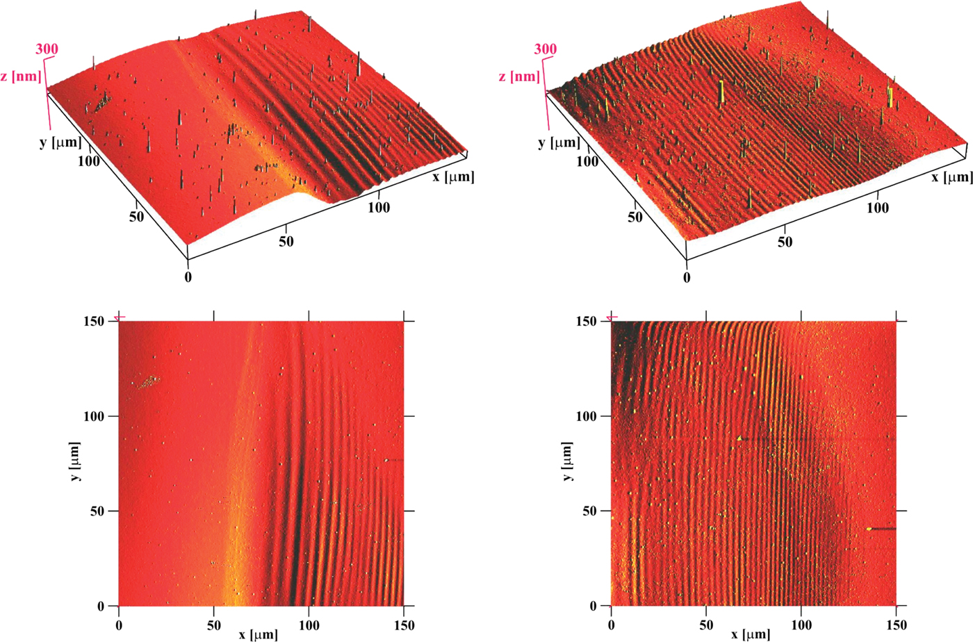
Fig. 5. (Color online) Spot ablated by five laser shots in the more distant astigmatic focus. (Left) region in the right corner. (Right) region in the middle-bottom part of the spot. (Top) 3D images. (Bottom) 2D images.
Similarly, ablation of PMMA samples with about 40 nm gold layer have also been analyzed by AFM (see Fig. 6). Left column of fields shows the upper part of the laser-beam-footprint. Both fields in this column were taken with AFM in taping mode; the upper field shows height, while the lower one shows phase contrast. Both fields indicate that in this case no periodic surface structure is created. Instead, units-of-micrometers-wide lighter part around the laser-beam-footprint in the lower field is interpreted as PMMA deposited on not-ablated gold layer. The same lighter surrounding around the laser-beam-footprint is visible in an enlarged scale in the middle-bottom-field (taken by AFM in current mode indicating local conductivity). Contrary, in the most enlarged scale (right column of the Fig. 6) no individual particles/grains/solidified-droplets of PMMA on Au were distinguishable (either in the upper field taken by AFM in taping mode measuring height, or in the lower field taken by AFM in current mode measuring local conductivity).

Fig. 6. (Color online) Analysis of laser-beam footprint on the gold (40 nm)-covered PMMA by AFM. (Left Column) upper part of the laser-beam-footprint; (Upper Field) AFM in taping mode indicating height; rectangle defines area shown in the middle column; (Lower Field) taping mode, phase contrast; (Middle Column: Upper Field) taping mode, height; rectangle defines area shown in the right column; (Lower Field) current mode. (Right Column: Upper Field) taping mode, height; (Lower Field) current mode.
Irradiation through a Small Grid
Finally, a surface of bare PMMA was irradiated through a small grid (step 12.5 × 12.5 µm, windows 7.5 × 7.5 µm) closely attached to this surface (see Fig. 7) with intention to see, if some structure similar to LIPSS is generated even in a limited space like a small grid window.

Fig. 7. (Color online) Bare PMMA ablated through the attached Au grid (step 12.5 × 12.5 µm, windows 7.5 × 7.5 µm). (Left) ablation by one shot. (Right) ablation by five superimposed shots. False colors.
Also this pattern was analyzed by AFM. It turned out that in each grid window a well-developed 2D diffraction pattern was created (see Fig. 8). The period of diffraction pattern changes from about 800 nm (at the edge of window) down to about 125 nm (in the middle of the window). One ridge (possibly a part of LIPSS) can be seen in the mid of the window.

Fig. 8. (Color online) AFM analysis of the ablated pattern in one grid window (dimension 7.5 × 7.5 µm). (Left) 3D plot. (Right) 2D plot.
Comparison of the ablated pattern with a theoretical profile of diffraction on a rectangular hole (see Fig. 9) confirms that the ablated pattern is really the result of diffraction.

Fig. 9. (Color online) Diffraction on the rectangular hole 7.5 × 7.5 µm; horizontal profile 5.3 µm.
CONCLUSION
It was demonstrated that our EUV Ar8+ laser (λ = 46.88 nm), the energy of which has not yet been reliably measured, but is estimated to be tens or hundreds of μJ is capable with focused beam to ablate PMMA (similarly to Juha et al., Reference Juha, Bittner, Chvostova, Krasa, Otcenasek, Prag, Ullschmied, Pientka, Krzywinski, Pelka, Wawro, Grisham, Vaschenko, Menoni and Rocca2005a), even if in our case the focus is significantly influenced by astigmatisms.
If the beam-footprint on a bare PMMA surface is large, the ablated area is covered by periodic surface structure with periodicity about 2.8 µm. However, it still remains to be proved, whether this pattern can be attributed to LIPSS.
If the beam-footprint on a PMMA, covered by a thin (about 40 nm) gold-layer, is large, no periodic surface structure has been observed. Instead, around the laser-beam-footprint a few micrometers wide composite area is created, where gold is intermixed with PMMA.
If the beam-footprint on a bare PMMA surface is small and limited by some obstacle, a diffraction pattern is created, the periodicity of which spans down to about 125 nm.
It should be mentioned that there is only a limited possibility to change the periodicity of these surface structures (if they are created). Therefore, a new interferometer is designed, which will be able to create controlled periodic structures with periodicity approaching the laser wavelength (about 50 nm in our present case, but with perspective of further reduction Kolacek et al., Reference Kolacek, Schmidt, Bohacek, Ripa, Frolov, Vrba, Straus, Rupasov and Shikanov2008a, Reference Kolacek, Schmidt, Prukner, Frolov and Straus2008b, Reference Kolacek, Prukner, Schmidt, Frolov and Straus2010).
ACKNOWLEDGMENTS
The experimental part of this work was performed under auspices and with the support of the Grant Agency of the Academy of Sciences CR (contract KAN300100702), the theoretical part of this work was supported by the Ministry of Education, Youth, and Sports of the Czech Republic (contracts LA08024 and LC528).


