


Introduction
In modern wireless and mobile communication systems, filters are always playing important and essential roles. To be suitable for application in modern communication systems, planar filters with compact size, high performance, and low cost are highly demanded [Reference Gan, He, Sun, Wei, Tang and Shi1]. Recently several microstrip bandpass filters (BPFs) have been reported. In [Reference Xu, Wang, Xu, Chen, Yu and Geng2], a capacitive gap and a Koch-shaped extended complementary single-split ring resonator pair have been used to suppress undesired harmonics and to enhance the frequency selectivity in the diplexer. As a result, an additional transmission zero is inserted above the upper edge passband of the left-handed transmission line (LH TL). Mezaal and Ali [Reference Mezaal and Ali3] describe a BPF using stepped impedance resonator (SIR) in order to isolate the second harmonic frequency in output frequency response of the filter. In [Reference Jantree and Akkaraekthalin4], it is noted that by using a cross-coupled structure, and a 0° feed structure (which has a 0° difference between the electric delays of the lower and upper paths), two transmission zeros in the stopband can be generated to improve the selectivity of the filter. However, these resonators have a large size and still exhibit harmonic responses. To overcome these problems, various methods have been investigated to suppress spurious harmonics and to reduce the overall circuit size by using a compact design. For example, based on composite right-handed transmission line/LH TL, fractal geometry in [Reference Xu, Wang and Liang5] and fractal shape in [Reference Xu, Wang and Zhang6] have been used to design BPFs. Based on the coexisting degenerate modes, two dual-band ring BPFs using four and eight open-circuited stubs loaded symmetrically along the ring have been achieved [Reference Luo, Zhu and Sun7]. The excitation angle is selected to be 45°. However, these two filters exhibit poor stopband rejection performance. SIR method can be used in the filter design in order to achieve a planar structure with compact size, to adjust the spurious passband to the higher frequency, and to isolate the harmonic frequencies [Reference Makimoto8]. Therefore, SIR method has been employed to achieve dual-band BPFs, such as SIR with the sinuous configuration in [Reference Sun and Zhu9]. Unfortunately, this dual-band BPF suffers from a poor selectivity in the stopband between its two bands. Thus, to compensate this deficient selectivity, a quarter-wavelength SIR implemented by an interdigital configuration in [Reference Chiou, Hsieh and Kuo10] and λ/4 SIR in [Reference Zhang and Zhu11] have been used to achieve dual-band BPFs. To generate extra transmission zero, researchers have paid attention to the coupling structures. For instance, mixed electromagnetic and capacitive source-load coupling have been used in [Reference Xiao, Li, Zhu, Zhao, Tian and Zhu12] to achieve single-band and dual-band BPFs in which the locations of transmission zeros are adjusted by controlling the magnitude of the electric and the magnetic couplings. Moreover, numerous approaches have been reported in the literature for multi-order spurious-mode suppression. Such as Hilbert-shaped complementary single-split ring resonator [Reference Xu, Wang, Zhang and Peng13], triangular SIR [Reference Chin and Chen14], cross-coupled spiral SIR [Reference Won, Bae and Myung15], split-mode excitations [Reference Lin, Li, Lin, Chen and Houng16], and composite series and shunt resonators [Reference Li and Wu17] have been used in microstrip BPFs. Dual-mode BPF, using slot superline technique [Reference Liu, Lei, Wan, Wang, Yang and Peng18], and meander resonator with rectangular-loop perturbation [Reference Chu, Mao and Zhou19] have been proposed. BPF filter, using discriminating coupling technique for extending out-of-band suppression has also been reported [Reference Li, Zhang and Xue20]. All the aforementioned works have the main objectives of reducing the occupied area and achieving high performances. However, nowadays these kinds of challenges are still existing in microwave passive circuit designs. Therefore, dual closed-loop stepped-impedance resonator is proposed to be investigated for application in the design of compact BPF.
In this paper, compact microstrip BPF using double dual closed-loop stepped impedance resonator (DCLSIR) is investigated and presented. The presented filter operates at X-band (9.3 GHz) with a fractional bandwidth (FBW) of 9.25%. Analysis based on the odd-mode equivalent transmission-line model of the presented resonator is given and design formulas are deduced. Different positions of the fundamental frequency, obtained by varying certain parameters of the resonator, are presented.
This paper is organized as follows. In the section “Design procedure”, the characteristics of the proposed resonator, the coupling coefficient, and the external quality factor of the DCLSIR are studied. Tuning of the center frequency, the position of the transmission zeros, and the bandwidth (BW) using physical dimensions of DCLSIR are also studied. In the section “Experimental results and discussion”, experimental results, discussions, and performance comparison between the presented work and the previous works are given. Finally, the conclusion is demonstrated in the section “Conclusion”.
Design procedure
Analysis of the proposed resonator
Figure 1(a) shows the basic structure of the DCLSIR. The proposed resonator is composed of two closed-loop SIRs connected together by a microstrip line L 1. The equivalent lumped-element circuit model of the proposed resonator in Fig. 1(a) is given in Fig. 1(b), where L 1 and L 2 are inductances, and C is a capacitance. Based on Fig. 1(a) and using the perfect electric and magnetic walls (A–A′), the odd- and even-mode equivalent transmission-line models are depicted in Figs 1(c) and 1(d), respectively. The odd-mode resonant frequency f o and even-mode resonant frequency f e of the proposed resonator are functions of the line lengths L o and L e, respectively, which can be expressed as:
 $$f_o = \displaystyle{c \over {L_o\sqrt {\varepsilon _{eff}}}}, $$
 $$f_e = \displaystyle{c \over {L_e\sqrt {\varepsilon _{eff}}}}, $$
where
 $$L_o = L_1/4 + (L_2 + L_3)/2,$$
 $$L_e = L_1/2 + (L_2 + L_3),$$
c is the light speed in free space and εeff is the effective dielectric constant of the substrate.
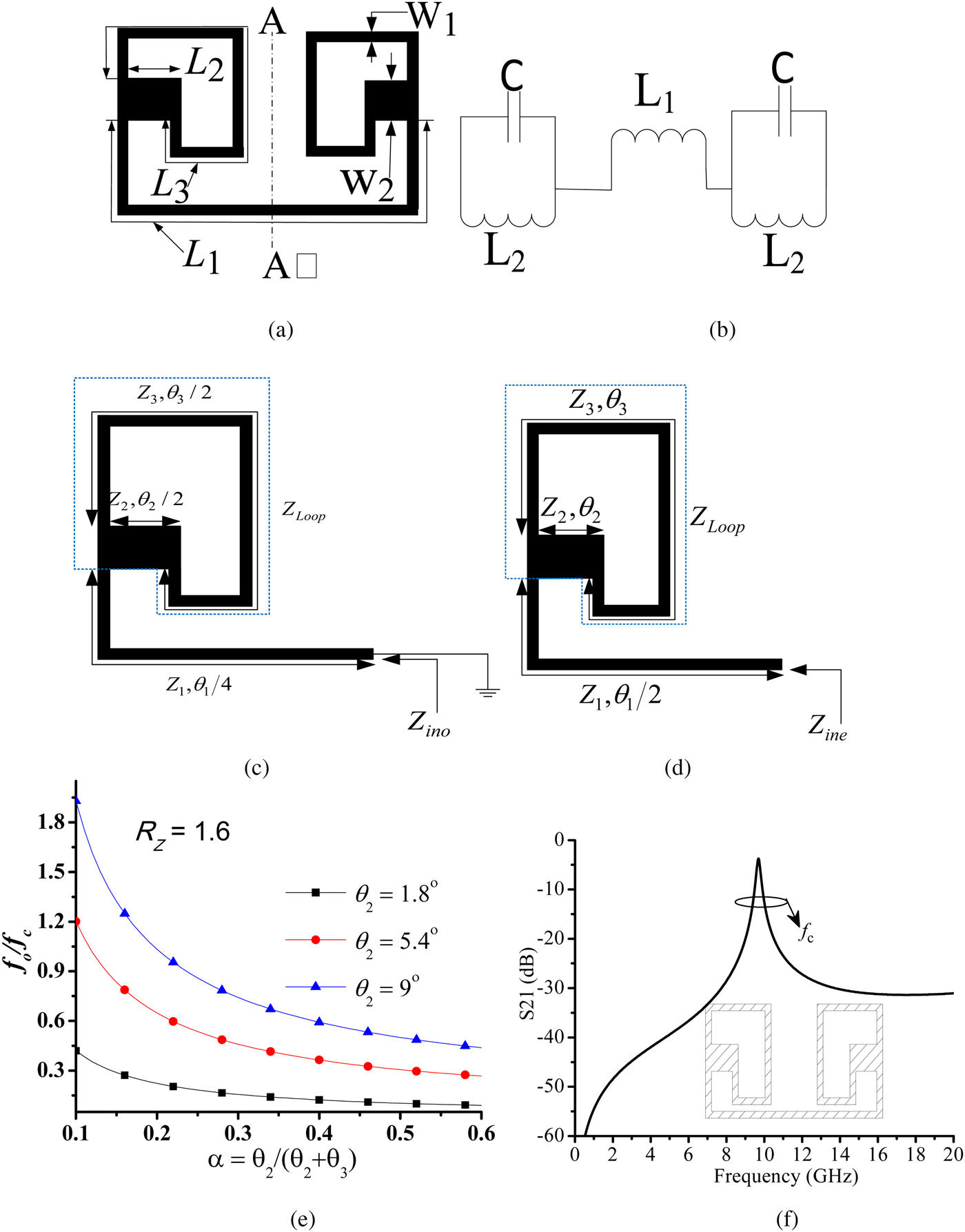
Fig. 1. (a) The proposed resonator, (b) equivalent circuit, (c) odd-mode equivalent circuit, (d) even-mode equivalent circuit, (e) normalized ratio f o/f c of the DCLSIR with R Z = 1.6, and (f) single-mode plotting.
Thereafter, only the odd mode has been considered to analyze the equivalent circuit and to deduce its resonant mode. By exciting odd-mode equivalent circuit from the perfect electric wall, the input impedance Z ino is deduced as [Reference Gan, He, Sun, Wei, Tang and Shi1]:
 $$Z_{ino} = Z_1\displaystyle{{Z_{loop} + jZ_1\tan \left( {\theta _1/4} \right)} \over {Z_1 + jZ_{loop}\tan \left( {\theta _1/4} \right)}}.$$
Inspecting Fig. 1(c), the loop part of the circuit consists of lower and upper sections that are composed of θ 2 and θ 3, respectively. The ABCD transfer matrices [Reference Yu and Chang21] for lower and upper sections (θ 2 and θ 3, respectively) are given in the following:
 $$\left[ {\matrix{ A & B \cr C & D \cr}} \right]_{lower} = \left[ {\matrix{ {\cos \theta _2} & {\,jZ_2\sin \theta _2} \cr {(\,j/Z_2)\sin \theta _2} & {\cos \theta _2} \cr}} \right],$$
 $$\left[ {\matrix{ A & B \cr C & D \cr}} \right]_{upper} = \left[ {\matrix{ {\cos \theta _3} & {\,jZ_3\sin \theta _3} \cr {(\,j/Z_3)\sin \theta _3} & {\cos \theta _3} \cr}} \right].$$
The Y-admittance matrices [Reference Yu and Chang21] for the lower and upper sections using the ABCD matrices are given in the following:
 $$\eqalign{& \left[ {\matrix{ {Y_{11}} & {Y_{12}} \cr {Y_{21}} & {Y_{22}} \cr}} \right]_{lower} = \left[ {\matrix{ {\displaystyle{D \over B}} & {\displaystyle{{BC - AD} \over B}} \cr { - \displaystyle{1 \over B}} & {\displaystyle{A \over B}} \cr}} \right]_{lower} \cr & \quad = \left[ {\matrix{ { - jY_2\cot \theta _2} & {\,jY_2\csc \theta _2} \cr {\,jY_2\csc \theta _2} & { - jY_2\cot \theta _2} \cr}} \right],} $$
 $$\eqalign{& \left[ {\matrix{ {Y_{11}} & {Y_{12}} \cr {Y_{21}} & {Y_{22}} \cr}} \right]_{upper} = \left[ {\matrix{ {\displaystyle{D \over B}} & {\displaystyle{{BC - AD} \over B}} \cr { - \displaystyle{1 \over B}} & {\displaystyle{A \over B}} \cr}} \right]_{upper} \cr & \quad = \left[ {\matrix{ { - jY_3\cot \theta _3} & {\,jY_3\csc \theta _3} \cr {\,jY_3\csc \theta _3} & { - jY_3\csc \theta _3} \cr}} \right].} $$
The resultant Y loop-admittance matrix is obtained by summing equations (7a) and (7b):
 $$\eqalign{& \left[ {\matrix{ {Y_{11}} & {Y_{12}} \cr {Y_{21}} & {Y_{22}} \cr}} \right]_{loop} = \cr & \quad \left[ {\matrix{ { - j\left[ {Y_2\cot \theta _2 + Y_3\cot \theta _3} \right]} & {\,j\left[ {Y_2\csc \theta _2 + Y_3\csc \theta _3} \right]} \cr {\,j\left[ {Y_2\csc \theta _2 + Y_3\csc \theta _3} \right]} & { - j\left[ {Y_2\cot \theta _2 + Y_3\cot \theta _3} \right]} \cr}} \right],} $$
then, the input admittance Y loop [Reference Yu and Chang21] (see Fig. 1(c)) can be deduced as:
 $$Y_{loop} = \displaystyle{{Y_{11}Y_{22} - Y_{12}Y_{21}} \over {Y_{22}}}.$$
Therefore, the characteristic impedance Z loop is deduced as:
 $$Z_{loop} = \displaystyle{{ - j\left( {Z_2\tan \theta _2 + Z_3\tan \theta _3} \right)} \over \matrix{\left( {(Z_2/Z_3) + (Z_3/Z_2)} \right)\left( {1 - {\tan} ^2\left( {\theta _2/2} \right)} \right) \hfill \cr \left( {1 - {\tan} ^2\left( {\theta _3/2} \right)} \right) + 4\left( {{\tan} ^2\left( {\theta _2/2} \right) + {\tan} ^2\left( {\theta _3/2} \right)} \right) \hfill}}. $$
By substituting Z loop in equation (5), the input impedance Z ino is deduced in the following:
 $$Z_{ino} = jZ_1\displaystyle{\matrix{\left( {1 + R_Z^2} \right)\left( {1 - {\tan} ^2\left( {\theta _2/2} \right)} \right)\left( {1 - {\tan} ^2\left( {\theta _3/2} \right)} \right) \hfill \cr \tan \left( {\theta _1/4} \right) + 4R_Z\left( {{\tan} ^2\left( {\theta _2/2} \right) + {\tan} ^2\left( {\theta _3/2} \right)} \right) \hfill \cr \tan \left( {\theta _1/4} \right) - \left( {\tan \theta _2 + R_Z\tan \theta _3} \right) \hfill} \over \matrix{\left( {1 + R_Z^2} \right)\left( {1 - {\tan} ^2\left( {\theta _2/2} \right)} \right)\left( {1 - {\tan} ^2\left( {\theta _3/2} \right)} \right) + \hfill \cr 4R_Z\left( {{\tan} ^2\left( {\theta _2/2} \right) + {\tan} ^2\left( {\theta _3/2} \right)} \right) + \hfill \cr \left( {\tan \theta _2 + R_Z\tan \theta _3} \right)\tan \left( {\theta _1/4} \right) \hfill}}, $$
where R Z is the impedance ratio, which is expressed as:
 $$R_Z = \displaystyle{{Z_3} \over {Z_2}} = \displaystyle{{Z_1} \over {Z_2}}.$$
Based on the resonance condition (Z ino = ∞), the resonant frequency of the proposed DCLSIR is deduced as equation (13):
 $$\eqalign{& \left( {1 + R_Z^2} \right)\left( {1 - {\tan} ^2\left( {\displaystyle{{\theta _2} \over 2}} \right)} \right)\left( {1 - {\tan} ^2\left( {\displaystyle{{\theta _3} \over 2}} \right)} \right) \cr & \quad + 4R_Z\left( {{\tan} ^2\left( {\displaystyle{{\theta _2} \over 2}} \right) + {\tan} ^2\left( {\displaystyle{{\theta _3} \over 2}} \right)} \right) + \cr & \quad \left( {\tan \theta _2 + R_Z\tan \theta _3} \right)\tan \left( {\displaystyle{{\theta _1} \over 4}} \right) = 0,} $$
where θ 1, θ 2, and θ 3 are the electric lengths of the DCLSIR.
From equation (13), by setting f o as the odd-mode resonant frequency and f c as the design frequency, then the design simplicity can be set as follows:
 $$f_o/f_c = 4\theta /\pi, $$
 $$\theta = \left( {\theta _2 + \theta _3} \right)/2 = \theta _1/4,$$
 $$\alpha = \theta _2/\left( {\theta _2 + \theta _3} \right),$$
where f o/f c and α are the normalized frequency ratio and electrical length ratio, respectively. It is found that from equations (13)–(16), there are several solutions for θ 2 and θ 3, which depend on the choice of impedance ratio R Z and electrical length ratio α. Figure 1(e) indicates the normalized ratio (f o/f c) versus the electrical length ratio (α) for the DCLSIR.
The proposed resonator is obtained by using the following steps:
Step 1, according to the specification frequencies of the design, choose f o/f c in Fig. 1(e) and then determine α.
Step 2, according to the known f o/f c, the design electrical length θ can be determined by equation (14).
Step 3, after knowing θ, the two electrical lengths (θ 1 and θ 3) can be determined by using equation (15).
In this work, f o/f c = 1.2 with R Z = 1.6 (Z 1 = Z 3 = 132.5 Ω, Z 2 = 83.99 Ω), and α = 0.17 (θ 1 = 108°, θ 2 = 9°, θ 3 = 45°) are fixed for generating the passband frequency response as shown in Fig. 1(f).
Design of BPF
With the center frequency f c = 9.3 GHz and the characteristic impedance Z 0 = 50 Ω I/O ports, the choice of the initial physical length of the proposed DCLSIR can be determined by the following equation [Reference Mezaal and Ali3]:
 $$\lambda _g = \displaystyle{c \over {\,f_c\sqrt {\varepsilon _{eff}}}}, $$
where λ g, c, and εeff are the guided wavelength, the light speed in free space, and the effective dielectric constant of the substrate, respectively. Figure 2(a) shows the initial layout of the proposed BPF, where the initial parameters (all in mm) are given as: W 0 = 1.1, L 1 = 3.81, L 2 = 0.65, L 3 = 3.74, L 4 = 2.71, L C = 1.8, W 1 = 0.1, W 2 = 0.4, S = 0.1, S 1 = 0.1, S 2 = 0.1. Figure 2(b) shows the EM simulated frequency response of the proposed BPF with initial parameters. As seen in Fig. 2(b), the center frequency f c has been shifted to 10.10 GHz and a spurious frequency response at the multiple of the center frequency f c has been observed in upper stopband at 21.70 GHz. Thus, to improve the performance at the upper stopband, two bended microstrip feed lines (BMFLs) at the input/output ports have been added as shown in Fig. 3(a). By cascading two DCLSIRs, a second-degree BPF is achieved. The two cascaded resonators are then coupled with the BMFLs. Figure 3(b) shows the coupling and routing scheme of the proposed filter in which the black circles 1 and 2 indicate resonators 1 and 2, respectively. The circles S and L indicate source and load, respectively, which are normalized to unity (g S = g L = g 0 = 1). The coupling coefficients between resonators (resonators 1 and 2) and BMFLs (source and load) are indicated by M 1S and M 2L, respectively. M 12 indicates the coupling coefficient between the two resonators, while M SL indicates the cross-coupling between source and load. The filter is designed based on approximate synthesis formulas [Reference Hong and Lancaster22] of the standard Chebyshev low-pass prototype filter, the elements are defined as: g 0 = 1, g 1 = 0.94286, g 2 = 1.36971, J 1 = −0.09019, and J 2 = 1.01563. According to the relationships between the bandpass design parameters and the standard Chebyshev low-pass prototype filter elements [Reference Hong and Lancaster22], the coupling matrix M ij of the filter is deduced as:
 $$M_{ij} = \left[ {\matrix{ {M_{SS}} & {M_{S1}} & {M_{S2}} & {M_{SL}} \cr {M_{1S}} & {M_{11}} & {M_{12}} & {M_{1L}} \cr {M_{2S}} & {M_{21}} & {M_{22}} & {M_{2L}} \cr {M_{LS}} & {M_{L1}} & {M_{L2}} & {M_{LL}} \cr}} \right],$$
 $$M_{ij} = \left[ {\matrix{ 0 & {0.0814} & 0 & { - 0.00885} \cr {0.0814} & 0 & {0.06859} & 0 \cr 0 & {0.06859} & 0 & {0.0814} \cr { - 0.00885} & 0 & {0.0814} & 0 \cr}} \right],$$
where M ij is the coupling coefficient of M 12 = M 21 = FBW × J 2/g 2, M SL = FBW × J 1/g 1, and  $M_{S1} = M_{2L} = FBW/\sqrt {g_1g_2} $. Thus, the coupling coefficient and external quality factor are found to be M 12 = 0.06859 and Q e = 10.81, respectively. By using full-wave EM simulation software, the coupling coefficient, as shown in Fig. 4(a), can be extracted using the following expression [Reference Hong and Lancaster23]:
 $$M_{12} = {{\left( {\,f_m^2 - f_e^2} \right)} / {\left( {\,f_e^2 + f_m^2} \right)}},$$
where f e and f m are the two splitting resonant frequencies obtained from full-wave EM simulation of the two identical coupled DCLSIRs. Also, the external quality factor, as indicated in Fig. 5, can be extracted using the following expression [Reference Hong and Lancaster22]:
 $$Q_e = {{\,f_c} / {\Delta f_{ - {\rm 3dB}}}},$$
where f c indicates the resonant frequency, and Δf −3dB is a 3 dB BW of the input or output resonator when it is alone excited externally. As seen in Fig. 4(a), for the fixed coupled length (L C = 1.7 mm), the coupling coefficient is decreased when the space coupling (S) is increased. The lower spacing coupling leads to mode splitting as shown in Fig. 4(b). The required space coupling can be set by choosing a large space between the two resonators as shown in Fig. 4(a). The external quality factor of the proposed filter can be set when the gap (S 1) is large enough as depicted in Fig. 5. The center frequency, the position of transmission zeros, and the FBW are functions of parameter L 1. By changing L 1 not only the center frequency but also the position of transmission zeros, and the FBW are changed as shown in Fig. 6. As indicated in Fig. 7, source-load coupling method has been employed to generate three transmission zeros. When the gap (S 2) between the source and the load is increased, TZ 2 and TZ 3 change their position, which means that the two transmission zeros can be affected by varying the value of S 2. According to the coupling matrix defined in equation (18), transmission zero TZ 1 has been created. Transmission zeros TZ 2 and TZ 3 are created due to the gap (S 2) between source and load.
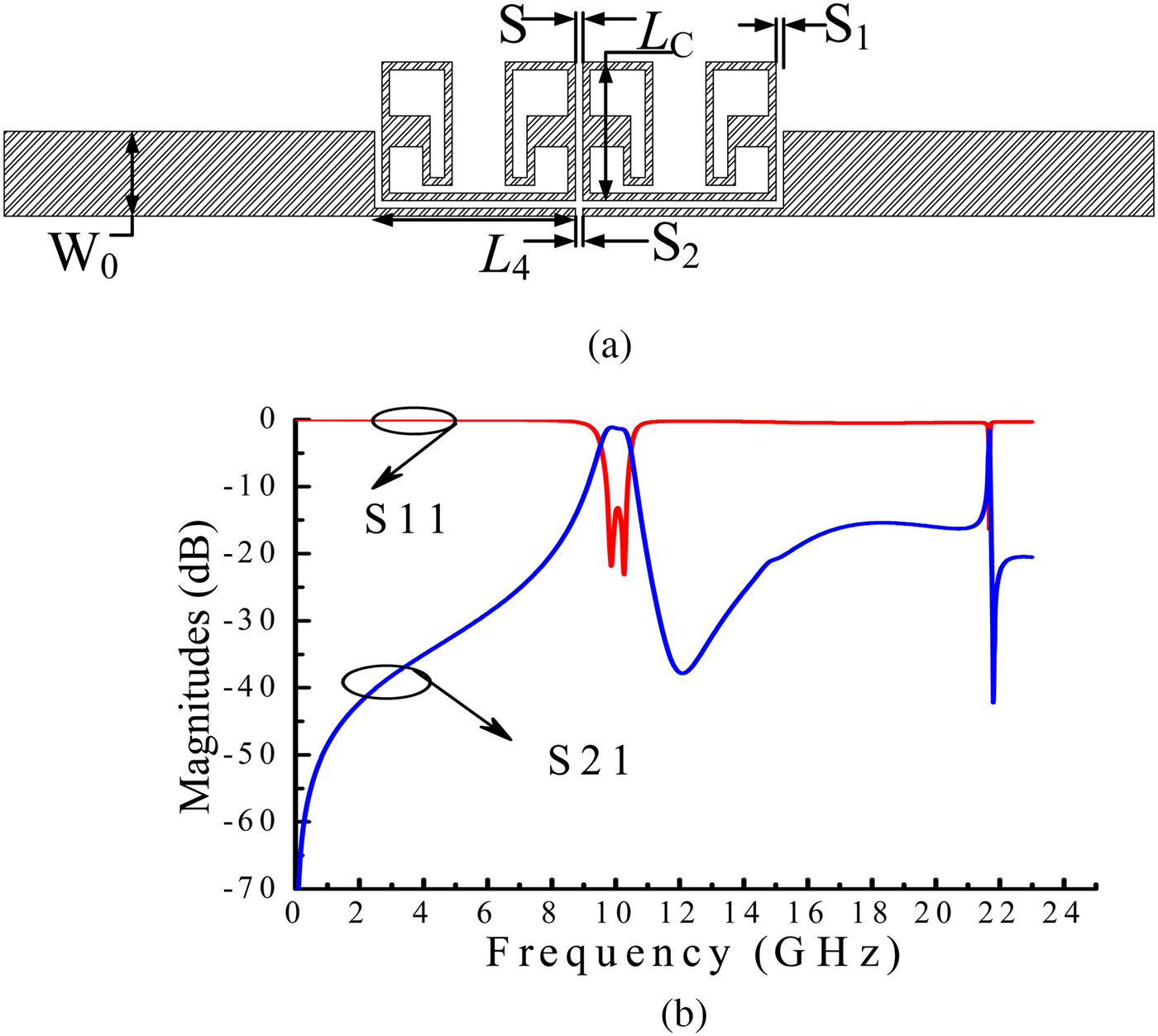
Fig. 2. (a) Layout of the proposed DCLSIR filter with initial parameters, (b) its EM simulated frequency response.

Fig. 3. The proposed DCLSIR filter: (a) layout, (b) its coupling scheme.

Fig. 4. (a) Coupling coefficient with varied coupling space (S), (b) frequency response of S 21 magnitudes with varied coupling space (S) under loose coupling.

Fig. 5. External quality factor with varied gap (S 1) between feeding line and resonator.

Fig. 6. EM simulated results with varied L 1, the inset part shows a close view of the passband.

Fig. 7. EM simulated results with varied S 2, the inset part shows a close view of the passband.
Experimental results and discussion
For verification of the predicted design defined above, a compact microstrip BPF using DCLSIR is designed and implemented on the Rogers RO4350 (tm) substrate with a height of 0.508 mm, a relative dielectric constant of 3.66, and a loss tangent of 0.004. The photograph of the proposed fabricated filter is given in Fig. 8. The structure of the proposed BPF is simulated by using HFSS software, the optimized physical dimensions (all in mm) are extracted as, L 1 = 4.2, L 2 = 0.655, L 3 = 3.965, L 4 = 7.07, L C = 1.7, W 1 = 0.1, W 2 = 0.4, S = 0.1, S 1 = 0.1, S 2 = 0.2. The measured results of the proposed filter are performed using Agilent E8363B Network Analyzer. The measured FBW is 9.25% at the center frequency of 9.3 GHz. The measured minimum insertion loss |S 21| including the loss from SMA connectors is 1.58 dB, while the measured return loss |S 11| is >17.7 dB. The insertion loss at ripple level ε and the return loss can be expressed in the following [Reference Hunter24]:
 $$IL = 10\log \,(1 + \varepsilon ^2) = 10\log \left( {\displaystyle{1 \over {{\left \vert {S_{21}} \right \vert} ^2}}} \right),$$
 $$RL = 10\log \left( {\displaystyle{1 \over {{\left \vert {S_{11}} \right \vert} ^2}}} \right) = L_R = 17.7{\kern 1pt} {\rm dB}{\rm.} $$
Fig. 8. Fabricated photograph of the proposed filter.
Then, from equation (22),
 $$\left \vert {S_{11}} \right \vert ^2 = 10^{ - L_R/10} = 0.01698$$
and
 $$\left \vert {S_{21}} \right \vert ^2 = 1 - \left \vert {S_{11}} \right \vert ^2 = 0.983.$$
Thus, the ripple level in the passband can be controlled by the level of ε, which can be deduced from equation (21) as:
 $$1 + \varepsilon ^2 = \displaystyle{1 \over {{\left \vert {S_{21}} \right \vert} ^2}}.$$
By using equations (24) and (25), the ripple level of the passband of the proposed filter is found as ε = 0.1315. Three transmission zeros TZ 1, TZ 2, and TZ 3 located at 10.7, 13.87, and 21.45 GHz, respectively, are created. Upper stopband attenuation |S 21| is better than 17 dB from 10.7 to 21.45 GHz. As illustrated in Fig. 9, the simulated and measured results are in good agreement. The observed slight deviation in the passband and stopband between the simulated and measured results might be due to the fabrication errors. The prototype DCLSIR BPF with a compact size of 0.17λ g × 0.031λ g (λ g is the guided wavelength of 50 Ω microstrip line on the substrate at the center frequency) satisfies the overall performances for X-band application. Table 1 illustrates the performance of the proposed filter with other previous reported works. As seen in Table 1, the proposed filter using DCLSIR has demonstrated a compact size as the major contribution of this work and lower insertion loss in the passband compared with [Reference Liu, Lei, Wan, Wang, Yang and Peng18–Reference Li, Zhang and Xue20]. However, it has larger insertion loss compared with [Reference Chu, Mao and Zhou19].

Fig. 9. EM simulated and measured results of the proposed filter, the inset part shows a close view of the passband.
Table 1. Performance comparison with the reported works

f c, Center frequency; IL, insertion loss; RL, return loss; TZ, transmission zero; Q e, external quality factor.
Conclusion
In this paper, a compact microstrip BPF based on the DCLSIR operating at 9.3 GHz for X-band application has been designed and fabricated. A cross-coupling theory has been employed to perform the upper stopband rejection. Better insertion loss and compact size of 0.17λ g × 0.031λ g are achieved. The proposed BPF exhibits favorable wide stopband performance. The compactness in circuit size makes the proposed design filter attractive for further developments and applications in X-band systems.
Acknowledgements
This work was supported by the National Natural Science Foundation of China (Grant No. U1430102).
 Salif N. Dembele received the M.S. degree in physical electronics from the University of Electronic Science and Technology of China (UESTC) in June 2015 and is now pursing his Ph.D. degree in electromagnetic field and microwave technology at the University of Electronic Science and Technology of China (UESTC), Chengdu, China, from September 2015. His research interests include microwave passive components design, RF MEMS technology, and circuits and systems.
 Ting Zhang received the M.S. degree in electronics and communication engineering from the University of Electronic Science and Technology of China (UESTC) in 2015 and is now pursing his Ph.D. degree in circuit and system at the University of Electronic Science and Technology of China (UESTC), Chengdu, China from 2015. His research interests include microwave planar multiplexer, filter, oscillator, RF MEMS switch, tunable filter, and microwave circuit.
 Jingfu Bao was born in Zhejiang, China, in 1964. He received his B.Sc., M.Sc., and Ph.D. degrees from UESTC, Chengdu, in 1986, 1989, and 1996, respectively, all in electronic engineering. In 1998, he was with SONY, Japan, where he worked on wireless RF circuit research until 2004. Since 2004, he has been with the School of Electronic Engineering, UESTC. Currently, he is a professor with the School of Electronic Engineering, UESTC. His research interests include MEMS technology, frequency synthesis, and high-frequency power amplifying device.
 Denis Bukuru received the M.S. degree in electromagnetic field and microwave technology from the University of Electronic Science and Technology of China (UESTC) in 2013, and Ph.D. degree in electromagnetic field and microwave technology at the University of Electronic Science and Technology of China (UESTC), Chengdu, China, from 2017. His research interests include microwave/millimeter-wave devices, circuits, and systems.


