


I. INTRODUCTION
The development of high–speed transistor technologies with increasing f max enables the design of active integrated circuits in the sub-millimeter-wave regions. State-of-the-art high electron mobility transistor (HEMT)–based monolithic microwave integrated circuits (MMICs) are pushing toward higher operating frequencies beyond 300 GHz. In the last few years, active integrated components such as mixers and amplifiers have been demonstrated [Reference Tessmann1–Reference Deal, Mei, Leong, Radisic, Sarkozy and Lai3]. Higher operatingfrequencies in radar or imaging applications enable higher image resolution due to the higher available absolute bandwidth and lower wavelength. Also high–speed communication systems will profit from increasing bandwidth with higher possible data rates.
All these components especially mixers and downconverters require signal sources to provide transmit signals or the local oscillator (LO) in frequency mixing applications. The generation can be realized by a phase–locked loop stabilized voltage–controlled oscillator, a fundamental oscillator or by multiplication of a high–quality, low phase-noise lower–frequency signal into the high–millimeter-wave range. In the case of frequency multiplication, the phase-noise will degrade by 20 log (N), where N is the multiplication factor of the frequency multiplier chain [Reference Camargo4]. Including the phase-noise degradation a multiplied signal still overcomes the noise performance of fundamental sources. A frequency multiplication approach transfers the advantages of lower–frequency generation such as faster frequency tuning, phase locking, and better phase-noise capabilities into higher–frequency regions. With this signal generation approach, digital synthesized signals could be multiplied into the millimeter-wave range leading to size and cost reduction. Although active frequency multipliers at high frequencies provide less output power as passive approaches, the technology features the possibility of integration with all functional blocks of a radar or communication system into one single MMIC. Providing the LO input at lower frequencies reduces the difficulty of packaging at sub-millimeter-wave frequencies. In terms of module integration, the manufacturing cost and complexity of a waveguide module scale with frequency.
To simplify the 300 GHz generation, a frequency tripler enables input frequencies at W-band (75–110 GHz). This frequency band today is easy to handle and high–quality frequency sources are commercially available for device testing. In this frequency regime integrated frequency multipliers based on metamorphic high electron mobility transistor (mHEMT) transistors are reported in [Reference Deal, Mei, Leong, Radisic, Sarkozy and Lai3, Reference Kallfass, Massler, Tessmann, Leuther, Schlechtweg and Weimann5, Reference Tessmann6], featuring possible frequency-tripler integration with further multiplication stages for 300 GHz millimeter-wave generation from Ku-, X-, or C-band input frequencies [Reference Kallfass, Massler, Tessmann, Leuther, Schlechtweg and Weimann5, Reference Lewark, Tessmann, Massler, Leuther and Kallfass7, Reference Weber, Lewark, Leuther and Kallfass8]. The X-band (8–12 GHz) in particular can provide commercially available solutions for large-scale system integration and direct digital synthesis (DDS) generation for fast frequency tuning. For a metamorphic HEMT doubler, the conversion losses reported in [Reference Kallfass9] are at least 7.4 dB. Nevertheless, the generation of W-band signals is much easier than 150 GHz signals due to commercially available solutions around the atmospheric window at 94 GHz and the increasing available power at lower frequencies. Therefore, the higher conversion loss is leveraged by easier or cheaper generation of the input signal or the possibility of multifunctional integration.
The major drawback of frequency multiplication is the generation of unwanted harmonics within the output spectrum. These harmonics appear as multiples of the input frequency ±n · f 0, where n ∈ ℕ. Mostly, at very high frequencies the output power is estimated by a total power meter. This measurement method integrates all harmonic powers of the output spectrum, hiding spurious responses within the output signal. In the doubler case, the fundamental tone will be suppressed by the waveguide cut-off but at higher multiplication factors the output signal contents several spurious lines. Based on the experimental results presented in [Reference Lewark, Tessmann, Massler, Wagner, Leuther and Kallfass10], we show measurements of the second harmonic power in H-band (220–325 GHz). In this frequency range mixers cannot be reliably calibrated. Therefore, the second harmonic power is calculated from a combination of two total power meter measurements using a waveguide high-pass filter.
II. METAMORPHIC HEMT TECHNOLOGY
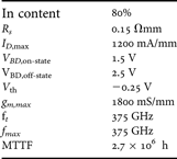
For high–frequency and low-noise applications, the Fraunhofer Institute for Applied Solid State Physics (IAF) has developed a mHEMT technology with a gate length of 50 nm [Reference Tessmann6, Reference Leuther11]. The transistor is based on an InGaAs/InAlAs heterostructure with high in content. For lower cost and quality, the HEMT structure is grown on 4″ semi-insulating GaAs wafers. For the metamorphic buffer, a linear InxAly Ga1−xAs (x = 0 → 0.52) transition is used. The electrons are confined in an ln0.80 Ga0.20 As/In0.53 Ga0.47 As composite channel, improving the breakdown behavior of the device. For high f max values and low-noise figure, a low gate line resistance is needed. Therefore, the T-gate uses a Pt/Ti/Pt/Au metallization.
For interconnects, an Au layer and a 2.7-µm–thick plated Au-layer in air-bridge technology are used. Further passive elements are NiCr thin–film resistors and MIM capacitors formed by the two metal layers and the SiN passivation as the dielectric layer. For the realization of MMICs operating at high millimeter-wave frequencies, a full backside process including wafer thinning to a final thickness of 50 µm was developed for the suppression of parasitic substrate modes. Through-substrate vias are etched with a diameter of 20 µm. Due to the high selectivity of the etching process the placement of the vias below MIM capacitors is possible.
The f t and f max values are extrapolated for a passivated mHEMT with 2 × 15 µm gate width. An overview of the electrical DC and RF parameters is given in Table 1.
Table 1. 50 nm mHEMT DC and RF parameters.
III. CIRCUIT DESIGN
Frequency multiplication conventionally is done by driving a non-linear device that converts the input power into a multi-harmonic signal. This device usually is a diode. Diodes are used up to the THz regime for frequency generation together with very high conversion losses and high integration cost. In this approach, the non-linear device is a FET amplifier stage under large-signal conditions. The choice of the generation type thereby plays an important role. There are two ways to generate harmonic output power with an amplifier stage. Most common is biasing the circuit under class AB or lower condition resulting in cutting parts of the sinusoidal input signal. For a frequency doubler the best bias condition is class B, creating a half–sinusoidal output waveform mainly consisting of even-order harmonics. The odd-order harmonic current at the drain is short-circuited by a λ/4 stub at the fundamental frequency. In and output have to be matched at the fundamental and the wanted harmonic frequency. Odd-order frequency generation also is possible by using a class A amplifier stage driven into deep saturation or under deep class B bias [Reference Maas12]. The sinusoidal input drive then is transformed into a trapezoidal waveform rich of odd-order harmonics [Reference Camargo4]. The major drawback is the needed high input power drive and therefore high conversion loss, which gets worse with increasing multiplication factor N. Another problem of a class A–type active frequency multiplier is the device gain at the fundamental tone. Short circuiting the fundamental current at the output leads to reflection of the amplified input signal. Either the input circuit has to be designed with a resistor for attenuating the reflected signal or the output matching needs a sink for the fundamental current. High reflection of the fundamental tone at the output of the circuit leads to an unwanted positive input reflection coefficient S11 and high risk of oscillation. At high frequencies, this effect gains importance due to the high influence of the parasitic gate drain capacitance. In the case of frequency tripling, we decided to use a common source FET amplifier stage under compressed class A operation. The first design step after choosing the basic circuit type is the device size. At very high frequencies a large gate width leads to high parasitic input capacitance but can handle more drain current and is able to deliver more output power. On the other side a high output power at this multiplier type leads to very high input power constraints. Therefore, the choice of the gate width is a trade-off between available output power and a low compression point. Very high input powers can lead to device damage by introducing a parasitic gate current up to mA scale, reducing dramatically the circuit lifetime and reliability. Based on advanced design system (ADS) simulations with the IAF large-signal transistor models a two finger device with a total gate width of 2 × 15 µm is used for optimum conversion performance at 100 GHz with a realistic available input power of 10 dBm at the input.
The input of the amplifier FET is matched to 50 Ω at the input frequency f 0 (IMN), while the output matching network (OMN) is providing conjugate complex matching at the third harmonic 3f 0. After that a band-pass filter (BPF) suppresses all unwanted harmonics at the output of the circuit. Figure 1 shows the frequency-tripler schematic. The input network is a bias-T, connecting the gate voltage V G to the transistor gate. (TRL) l 1 works as a shorted stub, RF grounded by C b. Within the OMN, the fundamental and second harmonic are reflected by either the BPF or by the very small series capacitor C OUT, building up a high-pass–type bias-T connecting the drain voltage. The resistor R suppresses the reflections and stabilizes the circuit representing a 50 Ω load for the fundamental tone. Without the resistor the reflected power leads to oscillations of the circuit due to the feedback of the parasitic gate drain capacitance of the common source mHEMT at high frequencies. This topology already is known from microwave frequency-tripler designs reported in [Reference Camargo4]. The loss introduced by the resistive load is reduced by a combination of two λ/4 transitions at the third harmonic. TRL l 2 converts an open circuit to a short circuit and, via TRL l 3, back to an open circuit at 3f 0. As the two λ/4 transitions represent an open circuit, the impedance still needs to be matched by l 4 and C OUT to 50 Ω.

Fig. 1. Schematics of the 300 GHz triplers, both based on a single mHEMT amplifier under compressed class A conditions.
The major filter stage is a coupled-lines–type filter. Starting values for field simulation in Ansoft's HFSS are found using simplified ADS coupled lines models. The distance to the electrical ground and the width of the coupled lines are optimized for impedance match to 50 Ω at the filter terminals for 300 GHz. Also the losses of the coupler have to be kept low for optimal conversion efficiency. Therefore, the conductor gap is optimized for minimal loss and adequate suppression at 2 f 0 and f 0.
Figure 2 shows a chip photograph of the frequency tripler MMIC. Its total chip size is 0.5 × 0.75 mm2, including RF and DC Pads. The grounded coplanar waveguide transmission lines have a reduced ground-to-ground spacing of 14 µm tapered at the RF pads.

Fig. 2. Chip photograph of the 300 GHz frequency-tripler realized in 50 nm mHEMT technology. The total chip size including DC and RF pads is 0.5 × 0.75 mm2.
Besides this chip, a slightly different version of the frequency tripler MMIC was processed. The circuit schematic is shown in Fig. 1(b). In this version the double λ/4 stub construction is replaced by a stub filter at the second harmonic (l 2) and a shorted stub–type transforming bias-T (l 3, C OUT). To encounter the introduced reflections from the output, the input network has to transform a much lower input impedance and therefore has longertransmission lines. The tripler operates with a compressed class A FET stage driven into input power saturation.
Showing the benefits of an active frequency multiplier concept the tripler is followed by a two–stage cascode amplifier with 10 dB gain in one single MMIC. Figure 3 shows the chip photograph of the integrated frequency multiplier. The total chip size of 1.25 × 0.5 mm2 is small enough for convenient integration into circuits with higher integration level within the Fraunhofer IAF's 50 nm mHEMT technology and represents a power source to drive sub-millimeter-wave mixers around 300 GHz with a W-band input.

Fig. 3. Chip photograph of the frequency-tripler MMIC integrated with an output buffer. The total chip size is 1.25 × 0.5 mm2.
IV. MEASUREMENT SETUP AND EXPERIMENTAL RESULTS
For the multiplier MMIC characterization on-wafer measurements are carried out comprising careful power–level normalization. Since the input and output power levels have to be normalized to the probe tip, the losses of the coplanar measurement probes in WR-3 band are defined using two WR-3 frequency extensions to a standard network analyzer. The input signal is generated with a commercial W-band source module extended by an in-house power amplifier, generating 10 dBm of input power from 95–105 GHz at the probe tip. Output power is measured by a total power meter (calorimeter). The most critical unwanted signal is the fundamental tone, which is suppressed totally by the WR-3 waveguide cut-off. Figure 4 sketches the characterization setup of the frequency tripler.
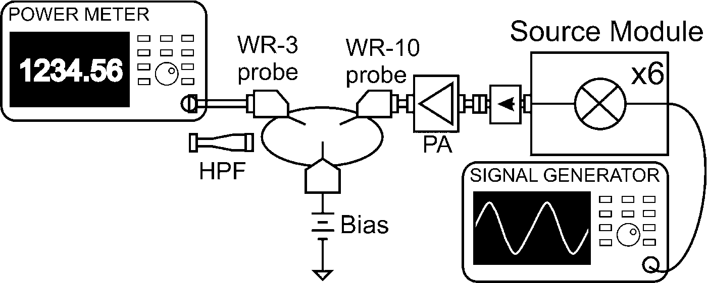
Fig. 4. On-wafer measurement setup for the 300 GHz frequency tripler. The power meter can be connected either directly or with a high-pass (HPF) filter to the WR-3 probe.
Assuming the conversion into higher tones than the third harmonic is negligible, the second harmonic may still be present within the WR-3 waveguide. For proving the presence of the third harmonic a waveguide type high-pass filter is introduced into the measurement setup. By estimating the total power with (P filt) and without (P tot) the filter, the power of the second harmonic P 2 can easily be calculated by taking the linear difference:
A) Stand-alone frequency tripler MMIC
A sweep of the input power at 100 GHz from 0 to 10 dBm reveals a saturated output power of −10.6 dBm at 300 GHz as shown in Fig. 5. At 10 dBm of input power, the circuit shows a conversion gain of −20.6 dB. Previous odd-order frequency multipliers with compressed class A transistor devices in [Reference Lewark, Tessmann, Massler, Leuther and Kallfass7] showed best output performance several dBs over the compression point, when the output signal turns more and more into a trapezoidal waveform. In the experiment shown in Fig. 5, this point is not reached, predicting higher available output power combined with higher conversion loss. The normalization of the input power takes into account the compression of the input power amplifier, therefore no more power could be applied and the measured saturation belongs to the device under test. At an input power of 4 dBm the conversion gain reaches its maximum of −18.5 dB, i.e. a conversion efficiency of 1.4%.

Fig. 5. Third harmonic output power at 300 GHz versus input power at 100 GHz (fundamental). The frequency tripler achieves a saturated output power of −10.6 dBm and a conversion gain of −18.5 dB.
Figure 6 shows the saturated output power versus input frequency for a constant input power level of 10 dBm. For proving the presence of the third harmonic two measurements have been taken. The first measurement without a WR-3 waveguide high-pass filter (black) reveals the saturated total output power of the chip. Unfortunately, the total power meter can only measure the sum of all harmonic power within the output spectrum. A second measurement canceling out the second harmonic power (red) by the high-pass filter shows a loss of 2 dB of output power around 300 GHz. This can be explained by a rising presence of the second harmonic in this frequency region. The calculated power of the second harmonic is also shown as the blue curve. The harmonic suppression is only adequate in the frequency regions where the two measurements show almost no difference. Around 300 GHz the suppression is only 3 dB, meaning that the second harmonic is present with half the power of the third. At lower and higher frequencies the suppression gets better than 10 dBc. The circuit presents a measured bandwidth of 285–315 GHz while the 3-dB bandwidth could not be measured due to the limited bandwidth of the power amplifier at the input of the measurement setup. The measured bandwidth already shows a relative bandwidth of at least 10%, i.e. an absolute bandwidth of 30 GHz. The input frequency sweep also reveals a maximum output power of −11.2 dBm and a sufficient suppression of unwanted harmonics below 288 and above 312 GHz. The comparison of the measured results and harmonic balance simulations (dashed lines) shows very good performance of the underlying large-signal models [Reference Seelmann-Eggebert, Merkle, van Raay, Quay and Schlechtweg13]. While the output power of the third harmonic is predicted correctly, the observed rising of the second harmonic power content was not predicted.

Fig. 6. Measured harmonic output power versus input frequency demonstrates a bandwidth of at least 285–315 GHz. The output power reaches its maximum at 303 GHz with −11.2 dBm.
Since the total bandwidth of the frequency tripler could not been measured due to the input power constraints, only a small part of the simulated bandwidth could be verified. Figure 7 shows a large-signal S-parameter simulation of the measured circuit. Large-signal S-parameters are normalized to the input frequency and are showing input matching at the fundamental (S11) and output matching at the third harmonic (S22). The gain (S21) represents the conversion gain of the tripler. Comparing the measured gain and the simulated S21 also shows a very good agreement between simulation and measurement. The simulated 3-dB bandwidth corresponds with large signal output matching and is simulated from 250 to 360 GHz, i.e. a relative bandwidth of 36%. The center frequency is 305 GHz.

Fig. 7. Large signal S-parameter simulation results of the 300 GHz tripler compared with the measured conversion gain (S21).
The frequency multiplier MMIC is fed by a single 1.2 V drain supply together with class A gate bias. At 10 dBm input power at an input frequency of 100 GHz, the MMIC consumes 14.4 mW (I = 12 mA) of DC power. Low DC power consumption and small chip size are important for further monolithic integration with other functional blocks of a system, such as mixers and amplifiers. At increasing input power level the FET gate diode starts to draw gate current. At further design steps the gate should be protected by a small resistance and within an application the device should not be driven into deep saturation. A parasitic gate current flow decreases the mean time to failure (MTTF) and degrades the device.
B) Buffered frequency-tripler MMIC
For the integrated tripler MMIC with buffer amplifier, a sweep of the input power at 288 and 300 GHz in Fig. 8 shows only a slight saturation behavior. At 12 dBm of input power, the output power still rises with 0.5 dB per dB of input power. Not compressing the amplification stage is very important because the amplifier used in this MMIC also has gain at second harmonic frequencies. Compressing it at third harmonic frequencies leads to lower suppression without significant gain of output power for the third harmonic content. Nevertheless in further designs a specially designed amplifier stage would be able to suppress the strong second harmonic signal around 300 GHz. Due to the gain of the amplifier the total conversion loss of the chip is reduced to a maximum of −11.4 dB at an input power of 5 dBm and an input frequency of 96 GHz. Like in the previous version, the conversion into the third harmonic is less efficient at 100 GHz input. At this frequency a significant part of the input power is transferred into the second harmonic.

Fig. 8. Measured harmonic output power versus input power of the buffered frequency tripler MMIC.
Comparing the sweep of the input power versus the output power of the stand-alone tripler and buffered tripler MMICs in Fig. 9 shows a power gain of 10.3 dB. At 6 dBm the amplifier gain decreases while the output power of the stand-alone tripler operates without significant saturation behavior. For this measurement the input power amplifier of the test setup could provide 16 dBm of power at the probe tip. At 16 dBm the tripler MMIC reaches saturation and shows a maximum output power of −7 dB without post-amplification. The integrated MMIC with output buffer provides 6.5 dB of gain and −0.5 dBm of output power providing a 0.9 mW sub-millimeter-wave power source.

Fig. 9. Output power versus input power of amplified and stand-alone frequency tripler MMIC. The output power reaches −0.5 dBm at 300 GHz.
At 288 GHz output frequency the MMIC generates a saturated output power of −0.5 dBm for an input power of 14 dBm (Fig. 10). The average output power is −1.9 dBm in the output frequency range from 285 to 315 GHz. For comparison with the stand-alone frequency-tripler, the output power of the amplified frequency-tripler is plotted with the same input power of 10 dBm (black). The frequency-tripler version implemented in the integrated version also has been characterized using the filter power measurement method revealing a small difference around 300 GHz (red). The result is shown in Fig. 10 including the calculated second harmonic content. Comparing the power levels of the stand-alone MMIC with the buffer MMIC the measurements reveal more than 11 dB of power gain by the two–stage buffer amplifier.

Fig. 10. Measured harmonic output power versus input frequency of both, amplified and stand-alone frequency-tripler MMICs.
The MMIC is fed by a 2 V drain and 1.2 V cascode and tripler drain supply together with class A gate bias. At 10 dBm input power and an input frequency of 100 GHz, the MMIC consumes 64 mW of DC power.
V. STATE-OF-THE-ART FREQUENCY MULTIPLICATION AROUND 300 GHZ
Since fundamental frequency generation around 300 GHz is suffering from low bandwidth and frequency stability only multipliers in different technologies are shown in Table 2. The highest output power is demonstrated with a passive heterostructure barrier varactor (HBV) drawing very high input drives of 1 W around 150 GHz together with high integration and packaging cost of diode technologies. Silicon bipolar technologies may have advantages in integration level but do not reach the band–width and low–noise operation of In-channel–based technologies. Therefore, silicon–based LO sources cannot overcome the packaging cost reduction and simplification together with a high–performing LNA.
Table 2. State-of-the-art frequency multipliers around 300 GHz.

Although the losses are high due to the ineffective conversion into odd-order harmonics with FETs [Reference Camargo4, Reference Maas12], the fast IAF mHEMT technology enables on chip amplifier integration. 13.5 dB of gain has been demonstrated at 300 GHz in [Reference Tessmann, Leuther, Massler, Kuri and Loesch2], respectively. The active approach of frequency multiplication, combined with ultra fast transistors, enables the integration with output buffer amplifiers on chip level even at sub-millimeter-wave output frequencies. Besides amplifier integration, more functionality can be integrated. The proof of this concept is an even higher integrated MMIC also including the presented tripler circuit. The on-chip buffer amplifier provides enough power for LO power generation around 300 GHz. The circuit in [Reference Tessmann, Massler, Lewark, Wagner, Kallfass and Leuther14] is an integrated down-conversion mixer with RF low-noise amplifier, while the LO of the fundamental mixer is provided by the presented buffered tripler MMIC. In this highly integrated MMIC the advantages of active frequency tripling result in a 300 GHz receiver with cost reducing W-band LO input together with the state-of-the-art low–noise performance of In–based HEMT low–noise amplifiers within the sub-millimeter wave regime.
VI. CONCLUSION
With the presented tripler MMIC frequency multiplication from W-band into H-band was demonstrated, enabling sub-millimeter-wave generation by easy to handle W-band signals. The realized tripler delivers −7 dBm of peak output power in a measured tuning range of at least 30 GHz within 285 and 315 GHz, whereas the 3-dB bandwidth could not be determined experimentally. Integrated with an output buffer amplifier, the presented frequency tripler shows an average output power of −1.9 dBm between 285 and 315 GHz and a peak output power of −0.5 dBm at 300 GHz. Power measurements with a waveguide filter are revealing the presence and power level of the second harmonic within the WR-3 waveguide. The benefits of an active multiplier approach are shown by the presented integrated MMIC.
ACKNOWLEDGEMENTS
We express our gratitude to our colleagues at IAF for their excellent contributions during epitaxial growth and wafer processing. We are particularly indebted to Michael Schlechtweg and Oliver Ambacher for their continuous support throughout this work.
 Ulrich J. Lewark was born in 1986. He received his Dipl.-Ing. degree in electrical engineering from the Karlsruhe Institute of Technology (KIT) in 2010. His diploma thesis on the topic of MMIC-based active frequency multipliers was carried out at the Fraunhofer Institute for Applied Solid-State Physics. He is now with the Institut für Hochfrequenztechnik und Elektronik (IHE) at the KIT as research and teaching assistant, where he is involved in the development of monolithic integrated circuits forradar imaging and broadband communication systems. His main research focuses on the development of frequency multiplier-chains for millimeter and sub-millimeter-wave signal generation.
 Axel Tessmann received the Dipl.-Ing. and Dr.-Ing. degrees in electrical engineering from the University of Karlsruhe, Germany, in 1997 and 2006, respectively. In 1997, he joined the High Frequency Devices and Circuits Department, Fraunhofer Institute for Applied Solid State Physics (IAF), Freiburg, Germany, where he is involved in the development of monolithically integrated circuits up to 340 GHz. His main research areas were the design and packaging of millimeter-wave ICs using high electron mobility transistors on GaAs, GaN, and InP, as well as circuit simulation and linear and non-linear device modeling. He is currently head of the millimeter-wave packaging and subsystem group at the Fraunhofer IAF.
 Hermann Massler was born in Radolfzell, Germany, in 1965. He studied electrical engineering at the Technical University Karlsruhe, Germany, where he graduated in 1993. While working on his diploma degree at the Forschungszentrum Karlsruhe (FZK), heperformed and investigated quasi-optical measurements at 140 GHz. He continued these studies as a FZK Research Assistant for an additional year. Since 1994, he has been with the Fraunhofer Institute for Applied Solid State Physics (IAF), Freiburg, Germany, working on transistor and IC characterization up to 325 GHz.
 Sandrine Wagner received a Bachelor of Science in Electronics and Informatics from the University of Mulhouse, France in 1989. She joined Micronas GmbH in Freiburg, Germany in 1989 where she was responsible for layout and physical verification of large–scale integrated semi-conductor devices. In 2010, she joined the Fraunhofer Institute for Applied Solid State Physics (IAF), Freiburg, Germany.
 Arnulf Leuther received the Dipl. Phys. and the Ph.D. degrees in physics from the Technical University of Aachen, Germany. In 1996, he joined the Fraunhofer Institute for Applied Solid State Physics (IAF), Freiburg, Germany. His research work is focused on the development of advanced III/V-process technologies for millimeter-wave and sub-millimeter-wave MMICs.
 Ingmar Kallfass received the Dipl.-Ing. degree in electrical engineering from the University of Stuttgart, Germany, in 2000, and the Dr.-Ing. degree from University of Ulm, Germany, in 2005. In 2001, he worked as a visiting researcher at the National University of Ireland, Dublin. In 2002, he joined the Department of Electron Devices and Circuits, University of Ulm, as a teaching and research assistant. In 2005, he joined the Fraunhofer Institute for Applied Solid State Physics. His current focus ison the design of non-linear millimeter-wave–integrated circuits for broadband communication systems and radar imaging.


