I. INTRODUCTION
Dual-mode resonators have been widely used to realize numerous radio frequency (RF)/microwave filters. The main feature and advantage of this type of resonator lies in the fact that each one of any dual-mode resonators can be used as a doubly tuned circuit and, therefore, the number of resonators required for an n-degree filter is reduced by half resulting in a compact filter configuration. The dual-mode microstrip filters can be performed either by two degenerate modes [Reference Wolff1] or non-degenerate modes [Reference Sheta, Dib and Mohra2]. In degenerate dual-mode case, the band-pass filter response can be obtained through: (1) excitation of the two degenerate modes by asymmetrical feed lines and (2) adjusting the coupling between the two modes by adding suitable form of perturbation within the resonators [Reference Goriir3, Reference Amari4]. The relative size and type of perturbation has direct effect on the bandwidth, and/or transmission zero location of a given dual-mode response [Reference Gorur5]. The dual-mode band-pass filter using square-loop or patch resonators has recently achieved circuitry size reduction while transmission zeros can also be easily introduced in the pass-band proximity to improve the filter selectivity. Recently, reconfigurable dual-mode band-pass filters have been investigated for tunable bandwidth applications [Reference Lugo and Papapolymerou6–Reference Tang and Hong11]. In this work, we present a circuit capable of producing a narrowband and a wideband response around the selected center frequency of 2.4 GHz. The filter requires no size compensation and the tunability is accomplished by two switches. The work presented in this paper demonstrates one fully reconfigurable filter with two states of operation, a narrowband and a wideband state including electronic switching by means of p-i-n diodes.
II. OPERATION THEORY AND PARAMETRIC STUDY
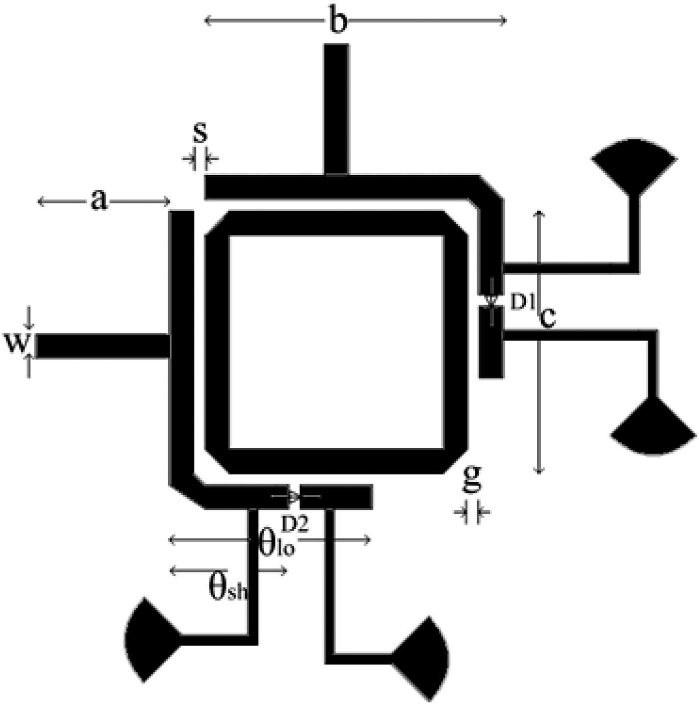
The proposed filter consists of a microstrip square-loop resonator with two L-shaped tuning stubs (Fig. 1). The overall length of the stubs dictates the coupling degree of the two degenerate modes, and is described by the coupling coefficient K. The fundamental principle dictates that the degeneration of the two modes and the resulted dual-mode filter will demonstrate wider bandwidth than the single-mode filter, as it has been verified in the insertion loss measurements shown in Section IV. The periphery of the rectangular microstrip ring is equal to one-guided wavelength at the center frequency (2.4 GHz).

Fig. 1. Schematic representation of proposed reconfigurable filter.
The figures of merit for resonator filters are the circuit's quality factors and the related coupling coefficients that need to be controlled in order to obtain the desired performance. The unloaded quality factor, Q 0 is defined in equation (1), and can be found in [Reference Chang and Hsieh12].
 $${Q_0}=\displaystyle{{{Q_L}} \over {\lpar 1 - {{10}^{ - L/20}}\rpar }}\comma$$
where L is the insertion loss in dB of the ring at resonance frequency and Q L is the loaded quality factor which is expressed in equation (2)
 $${Q_L}=\displaystyle{{{f_0}} \over {{{\lpar \Delta f\rpar }_{3dB}}}}.$$
The coupling between the L-shaped stubs and the ring can be expressed by the external quality factor (Q e) as follows:
 $${Q_e}=\displaystyle{{2{Q_0}{Q_L}} \over {{Q_0} - {Q_L}}}\comma$$
f 0 is the resonant frequency and (Δf)3 dB is the 3-dB bandwidth. In addition in this configuration, the coupling coefficient between two degenerate modes is given in equation (4) and is defined in [Reference Rouchaud, Madrangeas, Aubourg, Guillon, Theron and Maignan13],
 $$K=\displaystyle{{f_h^2 - f_l^2 } \over {f_h^2+f_l^2 }}\comma$$
where f h and f l are the higher and lower frequency return loss (S 11) resonances, respectively. The coupling coefficient between the two modes (K) exhibits three different coupling conditions. If K < (1/Q e + 1/Q 0) the coupling between the two modes is considered “under-coupled”, if K > (1/Q e + 1/Q 0) the coupling is “over-coupled” and in the case where K = (1/Q e + 1/Q 0) the coupling is “critically coupled”. In the presented case, it is worth noticing that for the dual-mode band-pass filter the coupling coefficient K is 0.012 and the expression (1/Q e + 1/Q 0) is 0.027; therefore, the under-coupling condition is satisfied.
If K is decreased, that is getting more under-coupling the bandwidth gets narrower. To obtain wide-band pass-band characteristic with the dual-mode ring a proper external quality factor and coupling coefficient K must be selected. Preferably a coupling coefficient with a value close to (1/Q e + 1/Q 0) would produce a wider bandwidth, as has been reported in [Reference Hsieh and Chang14].
A set of variables, namely θ, g, and s significantly affect the coupling the therefore the quality factors, and hence the bandwidth. The decided set of values was the result of the numerical optimization. In particularl, by adjusting the stub length θ and the tuning stub gap size, g, single-mode excitation or dual-mode excitation was produced accordingly. The bandwidth is also affected by the feeding stub gap, s. The following parametric study indicates the effect of the individual parameters in the insertion loss response. The structure of the proposed reconfigurable dual-mode band-pass filter is shown in Figs 1 and 2 shows simulated results for three cases from changing the gap size g with a fixed length (θ = 10 mm). Figures 3 and 4 show simulated results for three distinct cases from changing the stub length θ with a fixed gap size (s = 0.3 mm) and varying the gap size s with a fixed stub length (θ = 10 mm). In Fig. 2, both larger and smaller gap sizes than the chosen g = 2.4 mm result in narrower bandwidths. In Fig. 3, it is evident that longer stub length results in wider bandwidth. However, the total length is confined by the coupling coefficient K that needs not to exceed the critical coupling condition. Finally in Fig. 4, once again both smaller and larger sizes of gap s result in more narrow responses. In the s-parameter variation it is important to note that the right transmission zero remains constant in all three cases.
Fig. 2. Simulated |S 21| results for different g gap sizes with stub length θ = 10 mm.
Fig. 3. Simulated |S 21| results for different stub lengths θ with coupling gap s = 0.3 mm.
Fig. 4. Simulated |S 21| results for different gap sizes s with stub length θ = 10 mm.
The optimum set of values that result in the pass-band filter with the widest bandwidth has been a challenging attempt because the bandwidth dependence from the above parameters is not linear. Therefore, numerical analysis was necessary in order to control the coupling coefficient parameter that affects the loaded quality factor that defines the bandwidth.
III. RECONFIGURABLE FILTER DESIGN AND FABRICATION
A reconfigurable band-pass filter using a dual-mode microstrip square-loop resonator with switchable bandwidth is proposed, in which a square-ring is used as the resonator, and two microstrip tuning stubs are used as the perturbation elements. The filter is switched between different perturbation arrangement using two strategically placed p-i-n diodes capable of switching between a narrowband and a wideband response with two transmission zeros close to the pass-band. The proposed dual-mode filter topology is shown in Fig. 1 and Table 1 shows the fabricated filter dimensions.
Table 1. Dimensions of the fabricated filter.

The square-ring resonator with dimensions 18 mm × 18 mm is fed by a pair of perpendicular feed lines, and each feed line is connected to an L-shaped coupling arm that consists of a coupling stub and a tuning stub with the p-i-n diode. This asymmetrical structure perturbs the field of the ring resonator and excites two degenerate modes [Reference Lugo and Papapolymerou15].
Without the tuning stubs, there is no perturbation on the ring resonator and only a single mode is excited [Reference Lugo and Papapolymerou15]. The filter was designed on a 32-mil thick RO4003C substrate with a relative dielectric constant of 3.55 and tan δ = 0.0027.
The overall board size has dimensions 68 mm × 68 mm. The length of the tuning stubs is 4.5 mm for the narrowband state and 10 mm for the wideband state, the gap size between the feed lines and the ring resonator is 0.3 mm, and the gap size between the tuning stubs and the ring is 2.4 mm. Along the tuning stubs a 500 µm gap is left where the pin diodes are connected. Model MPND4005-B15 was used with dimensions 0.76 mm × 0.08 mm The PIN diodes D1 and D2 are used to switch between narrowband and wideband configurations. The narrowband state is produced when D1 and D2 are reverse biased. In this situation, a shorter stub is applied with length θsh = 4.45 mm and the narrowband state is implemented with a fractional bandwidth of 1.5%. On the other hand, when D1 and D2 are forward biased thus resulting in a longer stub θlo = 10 mm the wideband state is implemented with a fractional bandwidth of 4.8%. The DC bias lines are designed as RF chokes and consist of a high impedance 100 Ω transmission line terminated in an open radial stub for a total effective length of λ/2. The width of the DC bias lines is 0.45 mm with a total length of 23 mm. The dimensions of the proposed filter were optimized using numerical simulations in full-wave EM simulator Agilent Momentum.
In order to realize the electronic switching MPND4005-B15 planar beam lead PIN diodes by AEROFLEX METELLICS were used. The s-parameters of the PIN diodes were first measured in both forward and reverse bias states. Lumped element models were then created in order to match the s-parameters and simulate the effect of the PIN diodes on the topology [Reference Lugo and Papapolymerou15, Reference Wong and Hunter16]. The forward or “on” state of the diode from 1 to 4 GHz was equivalent to a 5 Ω resistor and produced an average insertion loss of 0.5 dB. The reverse-biased diode had an insertion loss of about 25 dB at the center frequency and the matching lumped element circuit consisted of a 0.03 pF capacitor. The modeled S-parameters are shown in Fig. 5. The filter was fabricated using standard photolithography and the p-i-n diodes were fixed to the board using silver epoxy in the 500 µm gap along the tuning stub. A picture of the fabricated filter is shown in Fig. 6. Figure 6 illustrates the fabricated reconfigurable filter during testing, with the bias lines to apply bias voltages to the circuit having the PIN diodes, implemented. All measurements were taken using a Rohde and Schwarz vector network analyzer.
Fig. 5. PIN diode transmission loss for both forward and reverse bias.
Fig. 6. Fabricated structure of the reconfigurable filter.
IV. MEASUREMENTS
The proposed filter was fabricated using photolithography and was tested using a Rohde and Schwarz vector network analyzer. Insertion loss, transmission loss, and group delay were measured for the two states of operation for both the hardwired filters and the switchable bandwidth filter with the two PIN diodes embedded, and appropriately biased.
The transmission and return loss of the wideband and narrowband states of the filter are shown in Figs 7 and 8, respectively, where measurements are compared to the simulated results. Good agreement can be observed between the measured and the simulated results. It can be seen that the measured transmission loss is higher than the simulated and this occurs because for the simulation the metal thickness was set to zero and perfect electric conductor was assumed in order to decrease the simulation time. For the simulation setup the PIN diodes were modeled as 5 Ω resistor for forward bias conditions and as a 0.03 pF for the reverse bias condition. In order to verify the predicted response of the filter and to assess the effect of the added switched hard wired filters were originally implemented. A longer stub was used to model the PIN diode in ON position and a stub with a gap was used to be compared to the PIN diodes in OFF position.
Fig. 7. Measured and simulated |S 21| and |S 11| parameters for wideband dual-mode filter.
Fig. 8. Measured and simulated |S 21| and |S 11| parameters for narrowband single-mode filter.
Figures 9 and 10 show the filter's measured response compared to filter with the ideal switches. Observing both figures it can be seen that the measurements with the diodes present a frequency shift of a few MHz compared to the ideal switches filters. PIN diode performance also seems to provide a lower unloaded quality factor. This is primarily attributed to the parasitics of the PIN diodes. Furthermore, the PIN diode adds approximately 0.25 dB insertion loss. The PIN diodes were biased using in series 1 kΩ resistor.
Fig. 9. Measured |S 21| of the wideband filter.
Fig. 10. Measured |S 21| of the narrowband filter.
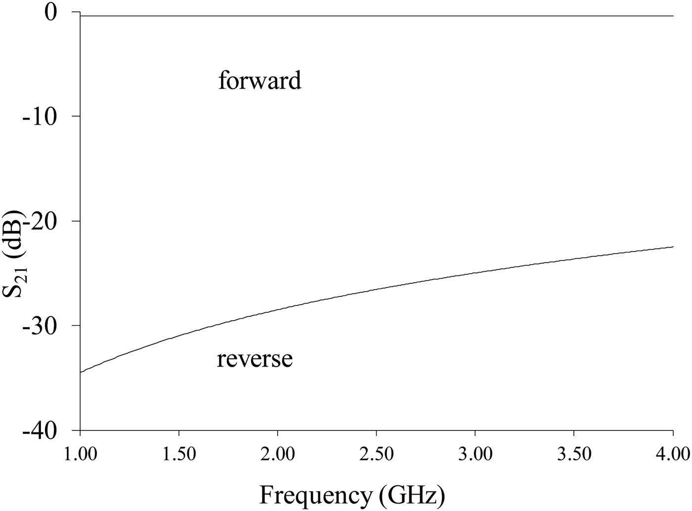
Figure 11 demonstrates the full operation of the switchable bandwidth filter with the implemented PIN diodes. It shows a comparison of the measured |S 21| of the narrowband (PIN diodes reverse biased) and wideband (PIN diodes forward biased) state of operation. The measured insertion loss of the filter in the wideband state was 1.2 dB at 2.4 GHz, whereas the insertion loss of the filter in the narrowband state was 1.5 dB, at the same frequency. The narrowband response exhibits a transmission zero located at 2.7 GHz and a bandwidth of 35 MHz (1.5% fractional bandwidth). The wideband state produced a bandwidth of 113 MHz (4.8% bandwidth) and two transmission zeros located at 2.28 and 2.51 GHz, respectively.
Fig. 11. Measured |S 21| for the switchable bandwidth filter.
Group delay for the reconfigurable filter can also be seen in Fig. 12. The dual-mode filter has a 3.8 ns group delay in the middle of the pass-band, with approximately 1 ns variation across the band. The delay response for the dual-mode filter shows spikes in the delay at the location of the two finite-frequency loss poles. These delay spikes are a result of a discontinuity in the phase of S 21 when crossing from one side of a loss pole to the other, and are of no physical significance [Reference Bell17].
Fig. 12. Measured group delay response of the reconfigurable filter.
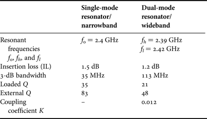
The measured performance for the single and dual-mode resonator is summarized in Table 2. At the reported operation states, the loaded quality factor Q L is 35 for the single-mode excitation that causes the narrowband state and 21 for the dual-mode excitation that causes the wideband state. This is calculated using the definition of Q L in equation (2).
Table 2. Performance of the reconfigurable filter.
Observing Table 2, in the case of the single-mode ring the higher external Q produces higher insertion loss and narrower bandwidth whereas for the dual-mode resonator the insertion loss and bandwidth depend on the external Q, the coupling coefficient and the coupling conditions.
V. CONCLUSION
A novel type of reconfigurable band-pass filter with switchable bandwidth, using a square-ring resonator with enhanced L-shaped coupling arms and PIN diodes as switches has been proposed. By switching the pin diodes OFF or ON the physical length and equivalent electrical length of the tuning stubs is modified thus achieving a single-mode filter with narrower bandwidth (35 MHz 3-dB bandwidth) or a dual-mode filter with wider bandwidth (113 MHz 3-dB bandwidth), respectively. The filter was designed with a center frequency at 2.4 GHz and the two states of operation demonstrated fractional bandwidth of 1.5 and 4.8%, respectively. The degeneration of two modes and hence the excitation of a dual-mode filter resulted in a more than three times, increased bandwidth, compared to the single mode, narrowband filter. Measurements verified the relatively low-loss performance of the filter with insertion loss better than 1.5 dB in the worst case, making the proposed filter a good candidate for the next generation, cognitive radios.
ACKNOWLEDGEMENT
The authors wish to thank the assistance of Dr. Arnaud Amadjikpe with the fabrication of the prototype device.
 Photos Vryonides received his Diploma, M.Phil., and Ph.D. degrees in Electrical and Electronic Engineering from the University of Manchester Institute of Science and Technology (UMIST), UK, in 1998, 1999, and 2002, respectively. Since 2007 he has been tenured track faculty member at Frederick University and Senior Researcher at Frederick Research Center (FRC). Dr. Vryonides is a member of the Microwaves and Photonics research group and his research interests span: mixers, LNAs, PAs, broadband amplifiers, millimeter-wave couplers, reconfigurable microwave filters, low-phase noise oscillators and millimeter-wave MMIC design, and components. Photos has authored or co-authored more than 40 papers in journals and peer-reviewed conferences.
Symeon Nikolaou received his Diploma degree in Electrical and Computer Engineering (Magna Cum Laude) from the National Technical University in Athens, Greece, in 2003 and the M.Sc. and Ph.D. degrees in Electrical and Computer Engineering from Georgia Institute of Technology, Atlanta, GA, USA in 2005, and 2007, respectively. Since 2007 he has been tenured track faculty member at Frederick University and Senior Researcher at Frederick Research Center (FRC). Dr. Nikolaou is a member of the Microwaves and Photonics research group and his research interests span: UWB antennas, passive and active RFIDs, wireless sensors applications, sensor integration with RFIDs, wearable antennas, reconfigurable antennas, and microwave imaging using UWB sensor arrays. Symeon has authored or co-authored more than 50 papers in journals and peer-reviewed conferences.
Sangkil Kim received his B.S. degree in Electrical and Electronic Engineering from Yonsei University, Seoul, Korea, in 2010, the M.S. degree in Electrical Engineering from the Georgia Institute of Technology, Atlanta in 2012, and was awarded the Ph.D. degree at the Georgia Institute of Technology in 2014. He is currently involved with the design and fabrication of novel wearable electronics for body area networks.
Tentzeris was born and grew up in Piraeus, Greece. He graduated from the Ionidios Model School of Piraeus in 1987 and he received his Diploma degree in Electrical Engineering and Computer Science (Magna Cum Laude) from the National Technical University in Athens, Greece, in 1992 and the M.S. and Ph.D. degrees in Electrical Engineering and Computer Science from the University of Michigan, Ann Arbor in 1993 and 1998, respectively. He is currently a Professor with the School of ECE, Georgia Tech and he has published more than 500 papers in refereed journals and conference proceedings, 4 books, and 23 book chapter. Also, Dr. Tentzeris is the Head of the A.T.H.E.N.A. Research Group and has established academic programs in Highly Integrated/Multilayer Packaging for RF and Wireless Applications using ceramic and organic flexible materials, paper-based RFID's and sensors, inkjet-printed electronics, nanostructures for RF, wireless sensors, power scavenging, and wireless power transfer, Microwave MEM's, SOP-integrated (UWB, multiband, and conformal) antennas, and Adaptive Numerical Electromagnetics (FDTD, MultiResolution Algorithms).