


I. INTRODUCTION
A common way to achieve a spatial resolution better than a few 100 nm in X-ray projection imaging is by using X-ray optics such as Fresnel zone plates. Although the use of these components can result in extreme high resolutions (Chu et al., Reference Chu2008), they are not always suited for tomographic imaging due to their very limited depth of focus. This limits the size of specimen that can be imaged in focus to a few microns (Suzuki, Reference Suzuki2008). To overcome this limitation while still retaining a nanometer-scale resolution, we investigated the achievable spatial resolution using X-ray sources with a nanofocus spot size. This approach has an infinite depth of focus.
One of the factors determining the smallest X-ray focal spot size attainable in an X-ray source is the type of electron gun used. Sources based on classical W filaments can achieve a focal spot diameter around <900 nm (Brunke, Reference Brunke and S. R.2008). When the electron beam is generated using a LaB6 crystal, X-ray spot diameters between 250 nm (Hamamatsu, 2009) and 400 nm (Tohken, 2009) have been reported. However, the smallest X-ray spot sizes are currently achieved using electron guns based on the Schottky field emission. These are often found in scanning electron microscopes (SEMs). Using a SEM as a nanofocus X-ray source, we studied the influence of X-ray energy and geometrical setup on the achievable spatial resolution.
II. EXPERIMENTAL SETUP
Figure 1 shows a schematic drawing of how a JEOL JSM-7000F SEM was used for X-ray imaging. A specimen holder is mounted on a rotation stage. The distance from the specimen to the target can be varied. The target is mounted at a 45° angle relative to the electron beam. The produced X-rays penetrating through the sample are acquired by direct detection in a cooled back-thinned charge-coupled device (CCD) camera (Princeton Instruments PIXIS-XO 512). This camera has 512×512 pixels and a pixel size of 24 μm. The electron gun is operated at 30 kV. The target can be coated with a thin substrate of a specific material to generate characteristic X-rays with appropriate energies.
III. RESULTS
A. First setup
To measure the resolution, we placed an XRadia resolution pattern X50-30-2 in the specimen holder. The resolution pattern has 180-nm-thick Au structures varying in size down to 50 nm. To provide a large geometrical zoom required to achieve a small image pixel size, the resolution pattern was placed at a distance of z 1=0.7 mm to the target. With a specimen-detector distance of z 2=25 cm this yields a zoom of 358× or an image pixel size of ∼67 nm. The target consisted of a 200 nm silver substrate layer deposited on 50 μm beryllium. Figure 2 shows a projection image of a part of the resolution pattern. The enlarged portion of the resolution pattern shows that the image contrast completely disappears at spatial frequencies corresponding to details of 300 nm. At even higher spatial frequencies the image contrast is inversed.
B. Diffraction limit
The loss and inversion of image contrast at high spatial frequencies seem to indicate that the Fresnel diffraction effects when X-rays pass through the resolution pattern start to

Figure 1. Schematic drawing of the SEM attachment that converts a SEM into an X-ray tomography system. The electron gun (1) shoots a narrow beam (2) onto a 45° target (3), producing an X-ray beam (4) passing though a specimen on a rotation stage at a variable distance from the target (5). The X-rays are detected by a cooled back-thinned deep depleted CCD camera (6).

Figure 2. X-ray projection image of an XRadia X50-30-2 resolution pattern. The enlarged portion shows a complete loss of contrast around 300 nm.

Figure 3. Computed X-ray spectrum as measured by the CCD when either an Ag (left) or an Au (right) target substrate is hit by 30 keV electrons. The Ag spectrum is rather monoenergetic around 3 keV, while the Au exhibits two strong peaks at 2.2 and 9.7 keV. The average energy of the Au spectrum is 6.4 keV.
become important. To verify this, the electromagnetic field strength in the detector plane was computed when an X-ray cone beam passes through a one-dimensional (1D) grid pattern. To compute the field strength U(x,y) we use the following equation (Cowley, Reference Cowley1990):
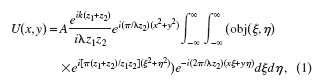
where obj(ξ,η) is the object transfer function (i.e., the absorption and phase shift of the X-rays when passing through the object), z 1 is the target to specimen distance, and z 2 is the specimen to detector distance. The influence of the X-ray focal spot size and the 24 μm CCD pixel size is taken into account by convolving U(x,y) with a Gaussian X-ray spot distribution and a 24-μm-wide block function.
The energy spectrum emitted by the Ag target substrate, as seen by the detector, is shown in Figure 3a. It was computed taking into account the X-ray emission spectrum emerging from the Ag target, the absorption in the 250 mm Be window in front of the CCD, and the wavelength depended detection efficiency of the CCD (Demers, Reference Demers2004). The spectrum observed by the detector is rather monoenergetic around 3 keV.
Figure 4 shows the computed response to a regular 1D grid patterns with different pitches. The width of the grid walls is equal to the pitch. The object transfer function assumes 180-nm-thick Au walls. The red periodic square patterns show the ideal response, while the blue sinusoidal-like curves correspond to the expected detector response taking Fresnel diffraction, X-ray spot size and detector pixel size into account. The complete loss of image contrast around 290 nm corresponds reasonably well with what we observed in the measured X-ray projection image.
C. Improved setup
From Eq. (1) one finds that there are two instrumental ways to improve the detectability of a smaller structure:

Figure 4. Predicted detector response to a regular 1D grid made of 180 nm Au walls. The pitch (=wall width) is varied from 260 to 340 nm.

Figure 5. Schematic drawing (left) and X-ray projection image (right) of the central portion of an ATN/XRESO-50HC (NTT-AT Nanofabrication Co.) resolution pattern.
• Reduce the defocusing distance z=(z 1×z 2)/(z 1+z 2). Since z 1⪡z 2 in our setup, it follows that z can be approximated by z 1, i.e., the target to specimen distance.
• Increase the mean X-ray energy.
These two enhancements were implemented in the following way:
• The distance between the resolution pattern and the target is reduced from 0.7 to 0.3 mm. To achieve this, the target had to be tilted from a 45° to a 75° angle. This results in an elliptical X-ray focal spot and hence the image resolution will be worse in one direction
• Replace the Ag target layer with an Au layer. This increases the mean energy from ∼3 to ∼6.4 keV.
• Improve contrast at these higher energies by replacing the XRadia resolution pattern with an ATN/XRESO-50HC (NTT-AT Nanofabrication Co.) resolution pattern. The latter has 500-nm-thick Ta structures.
In this new configuration we have a geometrical zoom of around 880× and an image pixel size of ∼27 nm. Figure 5 shows the central part of the NTTAT resolution pattern (left) and the resulting X-ray projection image (right). The resolution in the horizontal direction is better than the vertical resolution due to the tilt of the target. Structures of 200 nm are now still clearly visible. The details in the resolution pattern get wiped out when the sizes are less than ∼150 nm.
The computed energy spectrum as measured by the detector is shown in Figure 3b. It consists of three main peaks, M α (2.1 keV), L α (9.7 keV), and L β (11.4 keV), and a broad bremsstrahlung spectrum. Because the spectrum using the Au target cannot be considered monoenergetic, the prediction where complete loss of image contrast occurs is more complicated. The pitch at which complete loss of image contrast is expected in a 1D Ta grid with 500-nm-thick walls is shown in Figure 6 as a function of the X-ray energy. The observed diffraction limit around 150 nm is a result of the different components present in the energy spectrum. It follows from Figure 6 that a better suppression of the 2.2 keV M α peak and the low energy part of the bremsstrahlung spectrum (e.g., using slightly thicker Be window or a lower camera sensitivity at longer wavelengths) should push the point where we are diffraction limited towards 100 nm as the spectrum becomes more monoenergetic around 10 keV.

Figure 6. Predicted pitch of a regular 1D grid made of 500-nm-thick Ta walls where complete loss of contrast occurs.
IV. TRANSMISSION TARGET OPTIMIZATION
The use of a reflection-target geometry in our current setup prevents us from decreasing the target to specimen distance below 0.3 mm. The use of a transmission target could alleviate this restriction. Therefore a first Monte Carlo study was performed to minimize the X-ray focal spot size generated by a transmission target deposited on a 100 μm Be window. The simulations where performed using GATE (Jan et al., Reference Jan, Santin, Strul, Staelens, Assié, Autret, Avner, Barbier, Bardiès, Bloomfield, Brasse, Breton, Bruyndonckx, Buvat, Chatziioannou, Choi, Chung, Comtat, Donnarieix, Ferrer, Glick, Groiselle, Guez, Honore, Kerhoas-Cavata, Kirov, Kohli, Koole, Krieguer, van der Laan, Lamare, Largeron, Lartizien, Lazaro, Maas, Maigne, Mayet, Melot, Merheb, Pennacchio, Perez, Pietrzyk, Rannou, Rey, Schaart, Schmidtlein, Simon, Song, Vieira, Visvikis, Van de Walle, Wieërs and Morel2004) and focused on the optimization of the target.
Figure 7 shows the thickness dependency of the relative X-ray flux when either an Au or W target is irradiated with 30 keV electrons. When the thickness is less 200 nm, the electrons do not lose all their energy before escaping from the target material. This results in a reduced X-ray flux. On the other hand, when the thickness of the target material is too large (>500 nm), the X-rays produced within the target material have an increasing chance to be reabsorbed. Hence the best target thickness from an optimal X-ray flux point of view is around 300 nm.
The X-ray focal spot size is obtained from the distribution of points where the X-rays leave the target material, i.e., on the interface between the target material and the Be window. Only those X-rays that would eventually reach the CCD detector are taken into account. The focal spot size was characterized by two radii: a radius containing 50% of all X-rays emitted and another radius containing 90% of all X-rays emitted. For target thicknesses below 500 nm, the X-ray focal spot size grows with increasing target thickness (Figure 8). To achieve a sub-100-nm resolution, the target thickness should not exceed 250 nm to limit the contribution of the X-ray focal spot size.

Figure 7. Relative intensities of X-rays when Au and W transmission targets are irradiated with 30 keV electrons.

Figure 8. Focal spot size radii corresponding to the emission of 50% and 90% of the X-rays as a function of the Au target thickness. The electron energy was 30 keV.
V. CONCLUSION
Using a Schottky field emission electron gun in our JSM-7000F SEM to generate X-rays we can detect structures down to 150 nm in projection images of resolution patterns. This limit is probably imposed by the presence of the 2.2 keV photons of the Au M α line present in the energy spectrum seen by the detector. Tuning the detector response to higher energies should circumvent this limitation and improve the detectability towards 100 nm.
Another important parameter is the target to specimen distance. In the current setup it could not be made smaller than 0.3 mm. Using a transmission target deposited on a, e.g., 100 μm Be window allows us to reduce this distance further, thereby pushing the point of being diffraction limited to even higher spatial frequencies.
Hence, combining the above enhancements could open the possibility for sub-100-nm three-dimensional tomographic X-ray imaging with infinite depth of focus allowing the study of specimen with sizes much larger than a few microns.


