


I. INTRODUCTION
Thermoelectric (TE) materials that can realize the direct conversion between electric power and heat have promising applications in green renewable energy fields (Bell, Reference Bell2008). In last two decades, great progress has been made in traditional TE materials (Alama and Ramakrishna, Reference Alama and Ramakrishna2013; Bashir et al., Reference Bashir, Said, Sabri, Shnawah and Elsheikh2014; Dehkordi et al., Reference Dehkordi, Zebarjadi, He and Tritt2015; He et al., Reference He, Zhang, Zhang, Ji, Li and Zhao2015; Tan et al., Reference Tan, Zhao and Kanatzidis2016; Su et al., Reference Su, Wei, Li, Liu, Yan, Li, Su, Xie, Zhao, Zhai, Zhang, Tang and Uher2017), in which V2VI3 compounds TE materials are representatives (Rostek, Reference Rostek2015; Zhu et al., Reference Zhu, Hu, Zhao and He2016). The TE performance of the TE material is often determined by the dimensionless figure of merit defined as ZT = S 2σ T/κ, where S, σ, Τ, and κ are Seebeck coefficient, electric conductivity, absolute temperature, and thermal conductivity including the contributions of both carriers and phonons, respectively (Zhu et al., Reference Zhu, Luo and Liang2014). Decreasing the dimensionalities of TE materials has been demonstrated to be an effective way to improve the TE properties by reducing the lattice thermal conductivity and the enlarged ZT values have been achieved in some low-dimensional structures of traditional TE materials (Lin et al., Reference Lin, Sun and Dresselhaus2000; Bejenari and Kantser, Reference Bejenari and Kantser2008; Boukai et al., Reference Boukai, Bunimovich, Tahir-Kheli, Yu, Goddard and Heath2008; Wang et al., Reference Wang, Feser, Lee, Talapin, Segalman and Majumdar2008).
Bi2Te3-based V–VI compounds are the most important members of the near room-temperature TE material family. Up to now, much efforts have been devoted in Bi2Te3 among the Bi–Te system that includes different phases of the (Bi2)m(Bi2Te3)n homologous series, where m and n are numbers of Bi2 and Bi2Te3 blocks per unit cell (Bos et al., Reference Bos, Zandbergen, Lee, Ong and Cava2007; Reference Bos, Faucheux, Downie and Marcinkova2012; Loa et al., Reference Loa, Bos, Downie and Syassen2016). The preparation of Bi2Te3-based thin film has been reported by different techniques, including chemical vapor deposition (Boulouz et al., Reference Boulouz, Giani, Pascal-Delannoy, Boulouz, Foucaran and Boyer1998), pulsed laser deposition (Makala et al., Reference Makala, Jagannadham and Sales2003), electrochemical deposition (Li et al., Reference Li, Toprak, Soliman, Zhou, Muhammed, Platzek and Müller2006), Metalorganic vapor phase epitaxy (Kuznetsov et al., Reference Kuznetsov, Yapaskurt, Shchamkhalova, Shcherbakov, Yakushcheva, Luzanov and Jitov2016), and so on. The other phases of the Bi–Te system may appear in the deposition process of Bi2Te3 thin films. Bi4Te3 is less studied among Bi–Te compounds. The phase transition of the Bi4Te3 film grown in molecular beam epitaxy (MBE) system was reported that Te/Bi beam equivalent pressure ratio below 17 favor the formation of Bi4Te3 phase (Fülöp et al., Reference Fülöp, Song, Charpentier, Shi, Ekström, Galletti, Arpaia, Bauch, Lombardi and Wang2014). Bi4Te3 nanowires were synthesized on GaAs(111)B substrates with Au nanoparticles as the catalyst via MBE (Wang et al., Reference Wang, Lok, Wong and Sou2009) and Fletching-shaped Bi4Te3–ZnTe heterostructure nanowires were grown on Si substrates by physical vapor transport (Song and Kim, Reference Song and Kim2014). Micro-Raman spectroscopy study of Bi4Te3 films on Si substrates prepared by MBE has been reported (Xu et al., Reference Xu, Song, Pan, Chen, Wu, Lu, Gong and Wang2015). The above studies are mainly focused on the morphology or structure of the films, while their TE properties have not been reported before.
Bi4Te3 has a rhombic crystal structure with R-3 m space group (group number 166). The crystal structure of the Bi4Te3 unit cell is shown in Figure 1(a). The atomic layer is arranged in a sequence of –Te(2)–Bi–Te(1)–Bi–Te(2)–Bi–Bi–, i.e. one quintuple-layer of Bi2Te3 + two layer of Bi, along with the C-axis direction. The Te(2)–Bi is connected by a hybrid bond composed of the covalent bond and the ionic bond, and the Bi–Te(1) is a covalent bond. The connection between the seven atomic layers is the van der Waals force during the period of the crystal structure (Bos et al., Reference Bos, Zandbergen, Lee, Ong and Cava2007). The structure of Bi4Te3 can be viewed as a heterostructure formed by [–(Te(2)–Bi–Te(1)–Bi–Te(2)–Bi–Bi)–]3, which type of structure has been demonstrated to exhibit new topological insulator phenomena (Hirahara et al., Reference Hirahara, Bihlmayer, Sakamoto, Yamada, Miyazaki, Kimura, Blügel and Hasegawa2011).
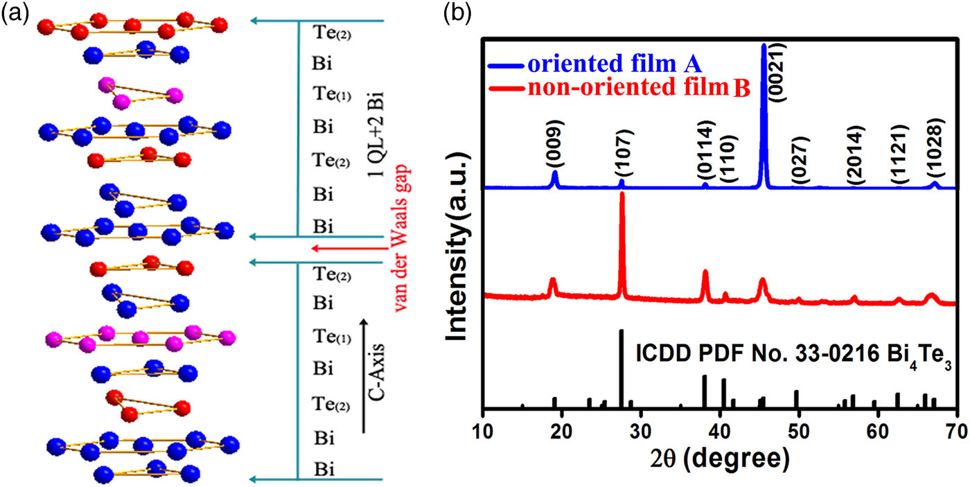
Figure 1. (Colour online) (a) The crystal structure of Bi4Te3 unit cell. (b) XRD patterns of the as-prepared two kinds of Bi4Te3 films A and B.
In this paper, we report the preparation of highly oriented nanopillars array Bi4Te3 films on SiO2 substrates by a vacuum thermal evaporation deposition technique. The electric conductivity and Seebeck coefficient of the Bi4Te3 films with different morphologies and orientations have been examined, and the improved electrical properties were revealed in the highly oriented nanopillars array Bi4Te3 film.
II. EXPERIMENTAL
A. Materials and methods
The Bi4Te3 films were deposited on SiO2 substrates using a high-vacuum thermal evaporation system. Firstly, the SiO2 substrates were ultrasonically cleaned in turn in diluted nitric acid, acetone, and alcohol to remove pollutants for 15 min, and then dried under the N2 flow. Commercial Bi2Te3 powder (99.98% purity, purchased from Aladdin) was used as the evaporation source. Then the source powder and the treated substrates were placed in the evaporating crucible and the substrate holder, severally. Both of the crucible and the substrate holder were fixed in a vacuum chamber that was evacuated to 1.0 × 10⁻⁴ Pa by a vacuum-pumping system. Two kinds of films with different morphologies and orientations were fabricated by adjusting the depositing parameters including the distance between the evaporation source and the substrate (called “distance” for short), source temperature and substrate temperature. The first kind of films (labeled as A) was fabricated by a distance of 5 cm, substrates 250 °C and source 520 °C. The second kind of films (labeled as B) was deposited by the distance of 10 cm, substrates 300 °C and source 500 °C. The deposition durations of both two kinds of films are 20 min.
B. Characterization
The crystalline phase and orientation of the films were characterized by X-ray diffraction (XRD, PANalytical PW3040/60) using Cu K α1 radiation (λ = 0.15406 nm). The top-surface and cross-sectional morphologies of the films were characterized by field-emission scanning electron microscopy (FE-SEM, Zeiss LEO1530VP). The electrical conductivity and Seebeck coefficient were characterized by LINSEIS LSR-3 in the in-plane direction at a temperature ranging from 339 to 584 K under a helium atmosphere. The measurement error for S and σ were both 5%. The carrier concentration and mobility were examined by the Hall test system from East Changing via a four-probe measurement.
III. RESULT AND DISCUSSION
A. Structural properties
Figure 1(b) illustrates the XRD patterns of the as-prepared Bi4Te3 films A and B. Both patterns can be indexed by rhombohedral phase Bi4Te3 with space group R-3m (ICDD PDF No. 33-0216), and no other phase of Bi–Te compounds is detected under the resolution of XRD. Obviously, the two films exhibit different texture as shown by their XRD patterns. Only the strongest (0021) reflection and the much weak (009) reflection can be easily identified in the XRD pattern of the Bi4Te3 film A, while other reflections can be hardly detected, which reveals its highly preferred (00l) orientation. As for the XRD pattern of film B, (107) reflection becomes the strongest, which is similar to that of standard diffraction data (ICDD PDF No. 33-0216). Meanwhile, (009), (0114), and (1028) reflections can be also easily seen, suggesting the non-oriented nature of film B. The slightly broadened shapes of the reflections should be related with crystalline sizes and quality (Tan et al., Reference Tan, Deng and Wang2014). The intense and profiles of XRD peaks can reveal the degree of crystallinity (χ c) of the films. We investigated the crystallinities of as-prepared films via the reference intensity ratio method (Prevey, Reference Prevey2000; Mu et al., Reference Mu, Zhou, He, Zhou, Wei, Zhu, Nie, Liu and Zhang2017):
 $$\chi_{\rm c} = \mathop \sum \nolimits^{I_{c}}/\left(\mathop \sum \nolimits^{I_{c}} + \mathop \sum \nolimits^{I_{a}}\right) \times 100\percnt,$$
where ∑I c is the sum of all the diffraction intensities and ∑I a is the sum of all the scattering intensities. The calculated results indicate that the oriented film A has much higher crystallinity (about 93%) than that of the non-oriented film B (about 66%). We further quantitatively examined the orientation degree (f) of the as-prepared films by Lotgering's method: (Lotgering, Reference Lotgering1959)
 $$f(00l) = (p - p_0 )/(1 - p_0 ),$$
 $$p = \mathop \sum \nolimits^{I}(00l)/\mathop \sum \nolimits^{I}(hkl),\quad p_0 = \mathop \sum \nolimits^{I_0} (00l)/\mathop \sum \nolimits^{I_0} (hkl),$$
where I and I 0 are the intensities of the reflections for the oriented sample and the non-oriented sample (standard diffraction data ICDD PDF No. 33-0216), respectively. The f values of the as-prepared Bi4Te3 films A and B are calculated to be 0.88 and 0.27, respectively, which quantitatively reveals the high (00l) preferential orientation of the as-prepared Bi4Te3 film and the controlled orientation of the films by adjusting the depositing parameters.
Figure 2 shows the top-surface and cross-sectional morphologies of the Bi4Te3 films A and B. Figure 2(a) presents the surface morphology of the oriented film A clearly indicating that the film is composed of a large number of regular-shaped grains with uniform sizes of about 150 nm. Meanwhile, the surface of the film is obviously smoother than that of the film shown in Figure 2(c). The cross-sectional SEM image in Figure 2(b) reveals that the film is composed of well-aligned nanopillars with diameters about 150 nm. It is worth noting that there is a buffer layer between the nanopillars array and the substrate consists of randomly distributed grains [as noted in Figure 2(b)]. From Figure 2(c), it can be seen that the non-oriented film B surface consists of irregular-shaped grains with non-uniform sizes ranging from nano to submicron scale. In addition, the heights of the grains are obviously non-uniform, and the larger grains are higher than the smaller ones. The cross-sectional view in Figure 2(d) indicates that the aggregation of the grains in the film is disorder, too. Based on the results of XRD and SEM, it can be concluded that highly (00l)-oriented nanopillars array Bi4Te3 film has been successfully fabricated by the vacuum thermal evaporation technique.
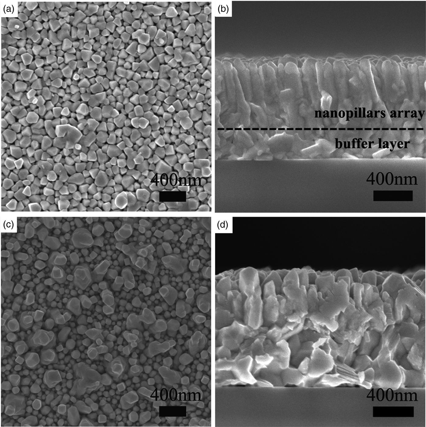
Figure 2. Top-surface and cross-sectional view FE-SEM images of Bi4Te3 film A (a, b) and Bi4Te3 film B (c, d).
B. Growth behavior
In this work, two issues are worthy of further discussions in the growth process of the Bi4Te3 films. The first one is why the as-prepared films here favor Bi4Te3 phase instead of the more thermodynamically stable Bi2Te3 phase. It has been revealed by some works that the phases of the compound films grown by vapor-phase growth systems are influenced by the compositions of vapor sources (Wang et al., Reference Wang, Lok, Wong and Sou2009; Fülöp et al., Reference Fülöp, Song, Charpentier, Shi, Ekström, Galletti, Arpaia, Bauch, Lombardi and Wang2014), which can be understood by the thermodynamic procedure of solid sublimation. The solid Bi2Te3 will disassociate into the vapor phase constituents of Bi and Te when evaporated under low pressure, and their evaporation rates will be influenced by the fractional coefficient K: (Wang and Wu, Reference Wang and Wu1990)
 $$K = \sqrt {m_{{\rm Te}} /m_{{\rm Bi}}} \exp [ - (\Delta H_{{\rm Bi}} - \Delta H_{{\rm Te}} )/RT],$$
where m Te, m Bi and ΔH Te, ΔH Bi are the molecular masses and vaporization heats of Te, Bi, respectively; R and T are the gas constant and the absolute temperature, respectively. The formula (4) shows that the greater the atomic mass, the greater the vaporization heat, the more difficult to evaporate. The fractionation coefficient K of Bi/Te was calculated to be about 0.325 at 500 °C, meaning the concentration of vapor phase Te atom is greater than Bi in the chamber. However, on the other side, the vapor species precipitate depending on the supersaturation degree that is related to the saturated vapor pressure of each kind of atoms (Chen et al., Reference Chen, Lan, Li, Cao and He2001a). It is known that the saturated vapor pressure of Te is much larger than that of Bi (10−2 Pa for Te and 10−9 Pa for Bi at a temperature of 250 °C) (Freeman and Edwards, Reference Freeman and Edwards1967; Honig and Kramer, Reference Honig and Kramer1969). Although the concentration of vapor phase Te atoms is higher than that of Bi, due to the large difference between their saturated vapor pressures, the precipitate rate of Te atoms on the substrate is still less than Bi atom in the present growth system, leading to the formation of Bi4Te3 films; and the Bi2Te3 films was obtained here at a relatively low evaporation source temperature (450 °C), which is consistent with the above discussion.
The second issue is the growth mechanism of the highly oriented nanopillars array Bi4Te3 film, which is schematically illustrated in Figure 3. It was found that the morphology and orientation of the grown films are mainly affected by the substrate temperature and the distance. The non-oriented ordinary Bi4Te3 film B is formed at the distance of 10 cm and the substrate temperature of 300 °C, while the highly oriented nanopillars array Bi4Te3 film A is formed at the distance of 5 cm and the substrate temperature of 250 °C. Briefly, in the early state of film growth, the vapor phase atoms from the evaporation source are impacted on the substrate and adsorbed thereon. The nucleation growth would be an island-like growth mode because the interaction between the atoms is greater than that between the atoms and the substrate (Kashchiev, Reference Kashchiev1977). The crystal nucleuses grow to form small-size particles, and then the grains expand randomly to form a buffer layer on the substrate. In the next state, the distance and substrate temperature would affect the deposition rate and growth direction. The collision between the subsequent vapor atoms is lower under the smaller depositing distance, resulting in a larger deposition rate. Meanwhile, the lower substrate temperature does not favor that the deposited atoms migrate laterally before the subsequent atomic deposition (Chen et al., Reference Chen, Li, Lan and Cao2001b). In addition, the source temperature plays an important role in the formation of the nanopillars array and the higher source temperature can cause a larger deposition rate facilitating the oriented growth. Combined the above effects, the one-dimensional growth along the (00l) direction vertical to the substrate is preferred to the lateral direction, resulting in the formation of the (00l) oriented nanopillars array Bi4Te3 film. In contrast, because of the larger distance and the higher substrate temperature, the vaporized atoms have sufficient time and energy to laterally grow in all directions to form the non-oriented ordinary Bi4Te3 film. The growth behavior of the Bi4Te3 films is consistent with that of Bi2(Te,Se)3 films reported before (Tan et al., Reference Tan, Deng and Wang2014).
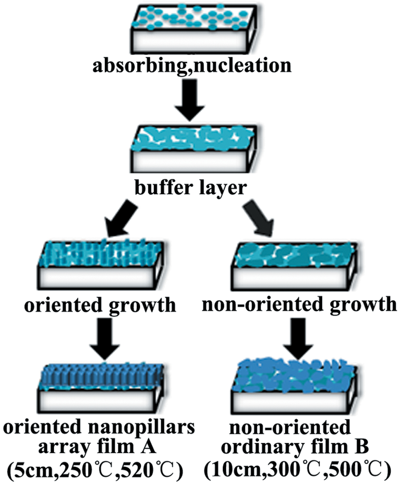
Figure 3. (Colour online) The growth mechanism of as-prepared two kinds of Bi4Te3 films A and B.
C. Electrical transport properties
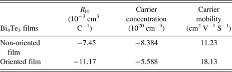
The room-temperature electrical transport properties of the Bi4Te3 films were listed in Table I. The negative Hall coefficient (R H) of the as-prepared films indicates their n-type conductivity. The carrier concentration of the non-oriented film is 8.384 × 1020 cm−3, which is slightly larger than 5.588 × 1020 cm−3 of the oriented film, while the values of their carrier mobility are 11.23 and 18.13 cm2 V−1 S−1, respectively, exhibiting an opposite trend. The reasons for the difference should be that the high orientation between the nanopillars benefits the carrier mobility by reducing the scattering at the grain boundaries. Considering the layered structure of Bi4Te3 along the (00l) orientation, the in-plane direction of the high (00l) oriented film provides faster channels for carriers transport compared with the non-oriented film. Moreover, the higher crystallinity for the oriented film would be of benefit to the carrier transport, too (Montgomery, Reference Montgomery1983; Mu et al., Reference Mu, Zhou, He, Zhou, Wei, Zhu, Nie, Liu and Zhang2017; Yin et al., Reference Yin, Zhang, Gao, Yao, Zhang, Han, Wang, Zhang, Xu, Zhang, Cao, Song and Jin2017). In addition, it is worth noting that the carrier concentrations of the Bi4Te3 films (~1020 cm−3) are much higher than those (~1019 cm−3) of BiTeSe (Tan et al., Reference Tan, Deng and Wang2014) and BiSbTe films (Chen et al., Reference Chen, Lin, Chang and Chen2017; Mu et al., Reference Mu, Zhou, He, Zhou, Wei, Zhu, Nie, Liu and Zhang2017), implying their much smaller Seebeck coefficients.
Table I. The room-temperature electrical transport properties of the Bi4Te3 films.
The dependence of the in-plane electrical conductivity σ, Seebeck coefficient S and power factor PF for the films in the temperature ranging from 339 to 584 K is shown in Figure 4. The electrical conductivities σ for the two films show the different temperature-dependence trend from 339 to 486 K and the σ for the oriented film is larger than that of the non-oriented film [Figure 4(a)], which is consistent with the result of Hall test. In this temperature region, the σ for non-oriented film decreases with increasing temperature, showing metallic conducting behavior, while the σ for oriented film keeps nearly constant, which suggests that the grain boundary scattering in the non-oriented film is more sensitive to temperature. From 486 to 584 K, the two films exhibit similar semiconducting behavior due to the thermal activation of carriers, and the increase of σ for the oriented film is larger than that for non-oriented film, revealing the more carriers activated. The negative Seebeck coefficient S of the as-prepared films also indicates their n-type nature, and the S of the oriented film is larger than the values of the non-oriented film [Figure 4(b)]. It should be pointed out that the S for the Bi4Te3 films is rather smaller than those for Bi2(Te,Se)3 films (Tan et al., Reference Tan, Deng and Wang2014), which can be accounted by their higher carrier concentrations as revealed by Hall test. It is known that S is proportional to n −2/3 (n is the carrier concentration) for metal or heavily doped degenerate semiconductors (Heremans et al., Reference Heremans, Jovovic, Toberer, Saramat, Kurosaki, Charoenphakdee, Yamanaka and Snyder2008). The decrease of S for the two films from 486 to 584 K shown in Figure 4(b) may be caused by the increase of carrier concentration or the bipolar effect that usually happens in high temperature (Goldsmid, Reference Goldsmid2016). The in-plane PF for the two films were calculated as shown in Figure 4(c). The PF of the (00l)-oriented film is 0.032 mWm−1 K−2 at 339 K, which is closer to twice that of the non-oriented film. Based on the results of the characterizations on structural and electronic properties, it can be concluded that the enhanced electrical performance in the oriented film is owing to the comprehensive effects caused by the high crystallinity and the order structures with well-controlled (00l)-preferential orientation.

Figure 4. (Colour online) Temperature dependences of (a) electrical conductivity, (b) Seebeck coefficient, and (c) power factor for the as-prepared oriented Bi4Te3 film (the blue squares) and non-oriented Bi4Te3 film (the red circles) along the in-plane direction.
IV. CONCLUSION
In summary, Bi4Te3 nanopillars films with high (00l)-orientation were successfully prepared on SiO2 substrate by a vacuum thermal evaporation deposition technique for the first time. The good control on the phase and microstructure of the Bi4Te3 films can be achieved by adjusting the growth parameters. The electrical transport properties of the Bi4Te3 films were investigated and the improved power factor was observed in the (00l)-oriented film compared with the non-oriented film.
ACKNOWLEDGEMENT
This work was financially supported by the National Natural Science Foundation of China (Grant nos 51472052 and U1601213).


