


1. INTRODUCTION
The compactness and miniaturization properties are playing a considerably important role in high-power nanosecond pulse generator (Nunnally, Reference Nunnally2005; Caballero & Smith, Reference Caballero and Smith2009; Tewari et al., Reference Tewari, Umbarkar, Agarwal, Saroj, Sharma, Mittal and Mangalvedekar2013). Besides, quasi-square pulses with their pulse width of several hundred nanoseconds would greatly benefit to the applications, which require high qualification electron beams such as X-ray flash radiography, high-power microwave, lasers, etc. Pulse forming line (PFL) and pulse forming network (PFN) are two main technologies to generate high-voltage quasi-square pulse with pulse duration of a hundred nanoseconds (Hammon et al., Reference Hammon, Lam, Drury and Ingram1997; Kekez, Reference Kekez2001; Sharma et al., Reference Sharma, Deb, Sharma, Shukla, Prabaharan, Adhikary and Shyam2012). However, if a pulse width >200 ns is required, a large volume of PFL system should be employed, even though spiral structure is applied (Zhang et al., Reference Zhang, Yang, Lin and Yang2013). Thus, PFN is a preferable way to generate long high-voltage quasi-square pulses.
A traditional PFN commonly consists of identical capacitors and inductors and it requires more than five network sections to generate quasi-square pulses (Li et al., Reference Li, Ryoo, Kim, Rim, Kim and Deng2009). Therefore, a traditional PFN always have a large volume. As shown in Figure 1, an N-section anti-resonance network, composed of different capacitors and inductors, consists of one-section LC series resonance network and (N−1)-section LC parallel resonance networks. Since the equivalent circuit of a typical Marx generator could be LC series resonance network, part of the anti-resonance network, it would be significant to carry out a study on the anti-resonance network to generate quasi-square pulse (Clementson et al., Reference Clementson, Rahbarnia, Grulke and Klinger2014). Only the first capacitor C 1 of the anti-resonance network need to be charged, which could lower the withstand voltage of the other capacitors.
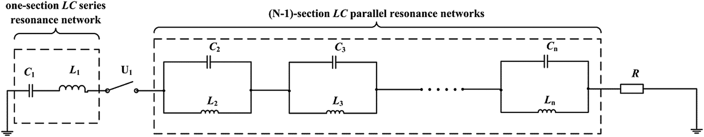
Fig. 1. Model of the N-section anti-resonance network.
A traditional anti-resonance network requires more than five network sections to generate more flat-topped and shorter rise-time pulses, thus making the whole system a large volume (White et al., Reference White, Gillette, Lebacqz, Glasoe and Lebacqz1948). Moreover, too many network sections make it difficult to adjust the inductors of the network to obtain ideal output pulses, which will make the PFN unreliable. Thus, fewer number of anti-resonance network sections is significant for the tendency of compactness and miniaturization of high-power pulse generators (Kim et al., Reference Kim, Mazarakis, Sinebryukhov, Volkov, Kondratiev, Alexeenko, Bayol, Demol and Stygar2012). But unfortunately, two- and three-section networks are rarely applied for it fails to output a flat-topped pulse.
In this paper, a method for designing parameters of two- and three-section anti-resonance networks which can generate quasi-square pulses was put forward for the compactness and miniaturization properties of the high-power generators. Fewer sections of the network can compact the structure of PFN and simplify the adjustment of the inductors to obtain ideal output pulses. A compact quasi-square pulse generator based on two/three-section anti-resonance network was presented. It is able to run in either two- or three-section network when its output pulse width is 400 ns. The results show that the improvements of the three-section over the two-section network are conspicuous as the rise time of the output pulse decreased from 90 to 60 ns, the flat top increased from 180 to 240 ns and the fall time decreased from 217 to 109 ns, consequently. Marx generators would be greatly benefited because this kind of network can be applied to shape the damped sine pulses generated by single Marx generators into quasi-square pulses. In this paper, a two-section anti-resonance network based on the four-stage Marx generator was designed and the output voltage on the resistive load of 50 Ω was 11.8 kV with a pulse width of 110 ns.
Section 2 makes an introduction of the method of parameter design as well as the simulation results in both two- and three-section networks. The design of the generator and the initial results are presented in Section 3. Section 4 presents its promising application in the Marx generator. Section 5 makes conclusions of this work.
2. THEORETICAL ANALYSES OF THE ANTI-RESONANCE NETWORK
2.1. Two-section network
According to the rule mentioned above, the two-section anti-resonance network is composed of one-section LC series resonance network and one-section LC parallel resonance network. The model of two-section anti-resonance network is displayed in Figure 2.
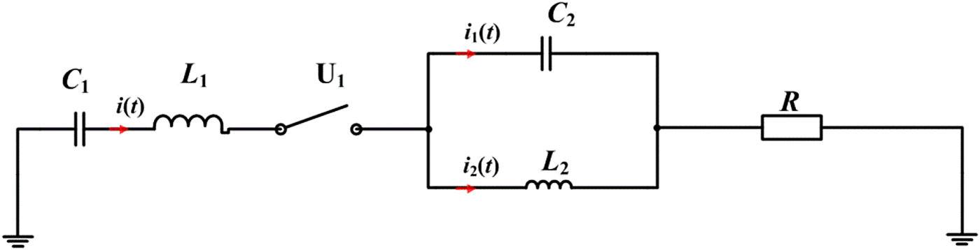
Fig. 2. Model of the two-section anti-resonance network.
In an anti-resonance network, only the first capacitor C 1 is active whereas the other capacitors, together with the inductors, are used for shaping the output pulse. Suppose C 1 has been charged before the switch U 1 close at the time t = 0, the equation for the circuit of Figure 2 could be
 $$\left\{ \matrix{U_{C_1} + L_1\displaystyle{{{\rm d}i(t)} \over {{\rm d}t}} + L_2\displaystyle{{{\rm d}i_2(t)} \over {{\rm d}t}} + Ri(t) = 0, \hfill \cr i(t) = i_1(t) + i_2(t), \hfill \cr L_2\displaystyle{{{\rm d}i_2(t)} \over {{\rm d}t}} = \displaystyle{1 \over {C_2}}\int_0^t {i_1(t){\rm d}t,} \hfill \cr U_{C_1} = U_0 + \displaystyle{1 \over {C_1}}\int_0^t {i(t){\rm d}t,} \hfill} \right.$$
where
 $U_{C_1}$
is the transient voltage on C
1, while U
0 is its initial voltage, R is the load resistance, i(t) is the current through the load, and i
1(t) and i
2(t) are the current through C
2 and L
2, respectively.
$U_{C_1}$
is the transient voltage on C
1, while U
0 is its initial voltage, R is the load resistance, i(t) is the current through the load, and i
1(t) and i
2(t) are the current through C
2 and L
2, respectively.
The corresponding Laplace transform of Eq. (1) could be
 $$\left\{ \matrix{\displaystyle{1 \over p}U_0 + \displaystyle{1 \over {\,pC_1}}I(\,p) + pL_1I(\,p) + pL_2I_2(\,p) + RI(\,p) = 0, \hfill \cr I(\,p) = I_1(\,p) + I_2(\,p), \hfill \cr pL_2I_2(\,p) = \displaystyle{1 \over {\,pC_2}}I_1(\,p). \hfill} \right.$$
The current through the load I(p) could be found from Eq. (2) to be
 $$I(\,p) = \displaystyle{{\,p^2C_1{\rm \alpha} _2 + C_1} \over \matrix{\,p^4{\rm \alpha} _1{\rm \alpha} _2 + p^3{\rm \alpha} _2{\rm \alpha} _3 + p^2 \hfill \cr \quad ({\rm \alpha} _1 + {\rm \alpha} _2 + {\rm \alpha} _4) + p{\rm \alpha} _3 + 1 \hfill}} ( - U_0),$$
where α1 = L 1 C 1; α2 = L 2 C 2; α3 = RC 1; α4 = L 2 C 1.
Now the key point is to shape the current through the load I(p) to be a quasi-square pulse. This is a purely mathematical problem. It can be perfectly solved by the Fourier theorem, which states that any waveform can be reproduced by the superposition of a series of sine and cosine waves. In particular, the constant function i(x) for 0 ≤ x ≤ π, defined as i(x) = 1, can be reproduced as follows:
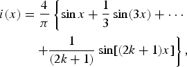 $$\eqalign{ i(x) &= \displaystyle{4 \over {\rm \pi}} \left\{ {\sin x + \displaystyle{1 \over 3}\sin(3x) + \cdot \cdot \cdot} \right. \cr & \quad \left. { + \displaystyle{1 \over {(2k + 1)}}\sin[(2k + 1)x]} \right\},} $$
where k = 0, 1, 2, 3, ….
Therefore, taking the initial voltage U 0, the characteristic impedance ρ and the frequency ω of the network into account, a quasi-square pulse can be reproduced in the form
 $$\eqalign{ i(t) &= \displaystyle{{4( - U_0)} \over {{\rm \pi \rho}}} \left\{ {\sin({\rm \omega} t) + \displaystyle{1 \over 3}\sin(3{\rm \omega} t) + \cdots} \right. \cr & \quad \left. { + \displaystyle{1 \over {(2k + 1)}}\sin[(2k + 1){\rm \omega} t]} \right\},} $$
where
 ${\rm \omega} = ({\rm \pi} /{\rm \tau );}\;k = 0,1,2,3, \ldots $
, τ is the pulse width of the network.
${\rm \omega} = ({\rm \pi} /{\rm \tau );}\;k = 0,1,2,3, \ldots $
, τ is the pulse width of the network.
Quasi-square pulses can be generated by the two-section anti-resonance network if the corresponding Laplace transform of Eq. (5) is similar to Eq. (3). Only the first two terms of Eq. (5) is needed due to this situation according to further calculations. Besides, the coefficients of the Fourier series expansion are helpful to shape the waveform of the pulses according to the previous studies. In conclusion, a quasi-square pulse can be reproduced as follows:
 $$i(t) = \displaystyle{{4( - U_0)} \over {{\rm \pi \rho}}} \left[ {\displaystyle{1 \over a}\sin({\rm \omega} t) + \displaystyle{1 \over b}\sin(3{\rm \omega} t)} \right].$$
Since
 $4( - U_0)/{\rm \pi \rho} $
is a constant, the waveforms of i(t) all depend on
$4( - U_0)/{\rm \pi \rho} $
is a constant, the waveforms of i(t) all depend on
 $y = 1/a{\rm sin}({\rm \omega} t) + 1/b{\rm sin}(3{\rm \omega} t)$
. The influences of a and b on y are shown in Figure 3. It is obviously that the top of the pulse flattens when a = 1, b = 9. However, the pulse width of a = 1, b = 9 is shorter than that of a = 1, b = 3, because the contribution of sin(3ωt) to i(t) is decrease when the value of b increase.
$y = 1/a{\rm sin}({\rm \omega} t) + 1/b{\rm sin}(3{\rm \omega} t)$
. The influences of a and b on y are shown in Figure 3. It is obviously that the top of the pulse flattens when a = 1, b = 9. However, the pulse width of a = 1, b = 9 is shorter than that of a = 1, b = 3, because the contribution of sin(3ωt) to i(t) is decrease when the value of b increase.

Fig. 3. Influence of a and b on the waveforms. (a) Influence of a; (b) Influence of b.
For a = 1, b = 9, the corresponding Laplace transform of Eq. (6) is
 $$I(\,p) = \displaystyle{{\,p^2(4 + (4/3)){\rm \omega} + (36 + (4/3)){\rm \omega} ^3} \over {\,p^4{\rm \pi \rho} + p^210{\rm \pi \rho} {\rm \omega} ^2 + 9{\rm \pi \rho} {\rm \omega} ^4}}( - U_0).$$
The output current of the two-section anti-resonance network is shown in Eqs (3) and (7) shows the expression of a quasi-square pulse. Obviously, the two equations are comparable for no significant differences in the numerator and denominator between them. Namely, parameters of the network could be found on condition that Eq. (3) is equal to Eq. (7). In this case, a comparison of the coefficients shows the parameters of the network to be
 $$\left\{ {\matrix{ {C_1 = 0.420\displaystyle{{\rm \tau} \over {\rm \rho}},} & {C_2 = 0.315\displaystyle{{\rm \tau} \over {\rm \rho}},} \cr {L_1 = 0.188\,{\rm \rho \tau},} & {L_2 = 0.046\,{\rm \rho \tau,}} \cr}} \right.$$
where τ is the pulse width, and ρ is the characteristic impedance of the network. Hence, parameters of the two-section anti-resonance network are only determined by the pulse width τ and the characteristic impedance ρ. According to the parameters shown in Eq. (8), the voltage waveforms for different load resistance were obtained in Figure 4 by PSpice software on the condition of ρ = 10 Ω, τ = 100 ns.

Fig. 4. Simulation results of voltage waveforms with different loads. (a) R = 10 Ω; (b) R = 1 Ω.
According to Figure 4, a small load makes top of the pulse flatter than a matched load. However, the pulse width will be a little shorter than expected as theoretical analysis shown in Figure. 3.
The effect of L 1 and L 2 on the output pulse is shown in Figure 5a, 5b, respectively. As shown in Figure 5, inductor L 1 has great effects on the rise time and fall time of the pulse, while inductor L 2 has great effects on the flat top and pulse width of the pulse. The rise time and fall time of the pulse would increase with the increase of the value of L 1, as shown in Figure 5a. To eliminate the overshoot of the pulse, the value of L 1 should be about 1.75 times greater than before as shown in Figure 5a. As shown in Figure 5b, the pulse width will increase with the increase of the value of L 2. It is found that the top of the pulse flattens and the pulse width is exactly 100 ns when L 2′ = 1.25L 2 from Figure 5b.

Fig. 5. Effect of L 1 and L 2 on the output pulse. (a) Effect of L 1 when L 2′ = L 2; (b) Effect of L 2 when L 1′ = 1.75L 1.
Therefore, modifications L 1′ = 1.75L 1, L 2′ = 1.25L 2 were put forward to eliminate the overshoot and increase the pulse width. The results after modifications are shown in Figure 6.

Fig. 6. Comparison of simulation results of two-section network before and after modifications.
Theoretically, the modifications are available to all values of τ and ρ, as is shown in Figure 7. Obviously, the ratio of the rise time to the base-to-base duration is a constant, so do the ratio of the flattop to the base-to-base duration.

Fig. 7. Simulation results of output voltage waveforms with different τ and R. (a) R = ρ = 10 Ω, τ = 100 ns; (b) R = ρ = 50 Ω, τ = 500 ns.
In conclusion, to obtain a quasi-square pulse on the matched load, the parameters of the two-section anti-resonance PFN are given by the equation
 $$\left\{ {\matrix{ {C_1 = 0.420\displaystyle{{\rm \tau} \over {\rm \rho}},} & {C_2 = 0.315\displaystyle{{\rm \tau} \over {\rm \rho}},} \cr {L_1 = 0.328\,{\rm \rho \tau},} & {L_2 = 0.057\,{\rm \rho \tau} {\rm.}} \cr}} \right.$$
2.2. Three-section network
Compared with two-section anti-resonance network, three-section network has one more section of LC parallel resonance network, as is shown in Figure 8.
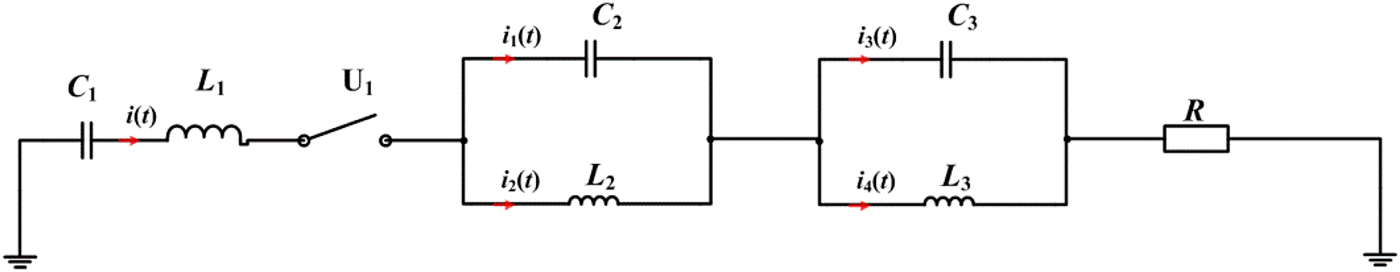
Fig. 8. Model of the three-section anti-resonance network.
In the same way, current through the load I(p) could be obtained as follows:
 $$\eqalign{I(\,p) &= ( - U_0)(\,p^4C_1{\rm \alpha} _2{\rm \alpha} _3 + p^2C_1({\rm \alpha} _2 + {\rm \alpha} _3) + C_1)/ \cr &\quad [\,p^6{\rm \alpha} _1{\rm \alpha} _2{\rm \alpha} _3 + p^5RC_1{\rm \alpha} _2{\rm \alpha} _3 + p^4({\rm \alpha} _1{\rm \alpha} _2 + {\rm \alpha} _1{\rm \alpha} _3 \cr & \quad + {\rm \alpha} _2{\rm \alpha} _3 + {\rm \alpha} _3{\rm \beta} _2 + {\rm \alpha} _2{\rm \beta} _3) + p^3RC_1({\rm \alpha} _2 + {\rm \alpha} _3)\cr &\quad + p^2({\rm \alpha} _1 + {\rm \alpha} _2 + {\rm \alpha} _3 + {\rm \beta} _2 + {\rm \beta} _3) + pRC_1 + 1],} $$
 $\eqalign{\hskip-1pc {\rm where}\quad{\rm \alpha} _1 &= L_1C_1,\;{\rm \alpha} _2 = L_2C_2,\;{\rm \alpha} _3 = L_3C_3, \cr {\rm \beta} _2 &= L_2C_1,\;and\;{\rm \beta} _3 = L_3C_1.} $
As the method mentioned above, a quasi-square pulse can be reproduced by the first three terms of the Fourier series expansion as follows:
 $$i(t) = \displaystyle{{4( - U_0)} \over {{\rm \pi \rho}}} \left[ {\displaystyle{1 \over a}\sin({\rm \omega} t) + \displaystyle{1 \over b}\sin(3{\rm \omega} t) + \displaystyle{1 \over c}\sin(5{\rm \omega} t)} \right],$$
where ω = π/τ, and τ is the pulse width of the network.
According to Eq. (11), the top of the pulse flattens when a = 1, b = 5, c = 30 based on Matlab software. Thus, the corresponding Laplace transform of Eq. (11) can be described as follows:
 $$I(\,p) = \displaystyle{\matrix{\,p^4{\rm \omega (}106/15{\rm )} + p^2{\rm \omega} ^3(34/a + 78/b + 50/c) \hfill \cr \quad + {\rm \omega} ^5(900/a + 300/b + 180/c) \hfill} \over \matrix{\,p^6{\rm \pi \rho} + p^435{\rm \pi \rho} {\rm \omega} ^2 + \hfill \cr \quad p^2259{\rm \pi \rho} {\rm \omega} ^4 + 225{\rm \pi \rho} {\rm \omega} ^6 \hfill}} ( - U_0).$$
Similarly, the parameters of the network were easily obtained based on Eqs (10) and (12) as follows:
 $$\left\{ {\matrix{ {C_1 = 0.435\displaystyle{{\rm \tau} \over {\rm \rho}},} \hfill & {L_1 = 0.142{\rm \rho \tau,}} \hfill \cr {C_2 = 0.450\displaystyle{{\rm \tau} \over {\rm \rho}},} \hfill & {L_2 = 0.011{\rm \rho \tau,}} \hfill \cr {C_3 = 0.250\displaystyle{{\rm \tau} \over {\rm \rho}},} \hfill & {L_3 = 0.067{\rm \rho \tau,}} \hfill \cr}} \right.$$
where τ is the pulse width, and ρ is the characteristic impedance of the network.
Modifications are also taken to obtain more flat-topped output pulse as the two-section network does. It is found that L 1′ = 1.45L 1, L 2′ = 1.1L 2, L 3′ = 1.27L 3 are the optimal modifications based on PSpice software. The comparison of simulation results of three-section anti-resonance network before and after modifications is shown in Figure 9 on the condition ρ = 10 Ω, τ = 100 ns.

Fig. 9. Comparison of simulation results of three-section network before and after modifications.
The parameters of the three-section anti-resonance PFN after modifications are given by the equation as follows:
 $$\left\{ {\matrix{ {C_1 = 0.435\displaystyle{{\rm \tau} \over {\rm \rho}},} \hfill & {L_1 = 0.206\,{\rm \rho \tau,}} \hfill \cr {C_2 = 0.450\displaystyle{{\rm \tau} \over {\rm \rho}},} \hfill & {L_2 = 0.012\,{\rm \rho \tau,}} \hfill \cr {C_3 = 0.250\displaystyle{{\rm \tau} \over {\rm \rho}},} \hfill & {L_3 = 0.085\,{\rm \rho \tau} {\rm.}} \hfill \cr}} \right.$$
2.3. Discussion about different sections anti-resonance network
According to the Fourier theorem, a better pulse shape needs more network sections, which can lead to a complicated system. Thus, fewer number of network sections is significant for the tendency of compactness and miniaturization of high-power pulse generators. Besides, fewer number of network sections leads to obtain ideal output pulses through adjusting inductors of the network easier and make the PFN more reliable.
Figure 10 shows the comparison of simulation waveforms of the output pulse between two- and three-section anti-resonance networks. Obviously, three-section network has a faster rise time, a longer flat top and a faster fall time compared with two-section network.

Fig. 10. Comparison of simulation waveforms of output pulses between two- and three-section networks.
Specifically, the simulation results show that the flat top of the two-section's output pulse is about 25% of the base-to-base duration, while the rise time is about 14% and the pulse width is about 67% comparing with the three-section network's 45, 11, and 80%, respectively. The improvements of the three-section over the two-section network is conspicuous.
Therefore, two-section network is more appropriate to the applications with pulse width <100 ns, while three-section network is well adaptable to more range of applications with pulse width from tens of nanoseconds to hundreds of nanoseconds.
3. EXPERIMENTAL SETUP AND INITIAL RESULTS
3.1. Experimental setup
It is known that the compact high-power pulse generators require the capacitors to have a high relative permittivity and withstand voltage. With the development of the fabrication technique of the capacitor these years, the self-inductance of the ceramic capacitor has been significantly reduced and the DC voltage that a single cell could withstand has been up to 50 kV (Domonkos et al., Reference Domonkos, Heidger, Brown, Parker and Gregg2010; Pan & Randall, Reference Pan and Randall2010), which make the ceramic capacitor a promising energy storage unit for compact pulse power devices. Meanwhile, quasi-square pulses with pulse width of hundreds of nanoseconds have many applications, such as sterilization of micro-organism, dispose of plant cells, transformation of industrial waste gas, and so on. Hence, a quasi-square pulse generator based on ceramic capacitors and two/three-section networks is designed in this paper. For two-section anti-resonance network pulse generator, if the pulse width is τ = 400 ns and the characteristic impedance of the network is ρ = 20 Ω, the parameters of the network can be easily obtained from Eq. (9) as follows:
 $$\left\{ {\matrix{ {C_1 = 8.4\,{\rm nF},} & {L_1 = 2.6\,{\rm \mu H,}} \cr {C_2 = 6.3\,{\rm nF},} & {L_2 = 456\,{\rm nH}{\rm.}} \cr}} \right.$$
As for the three-section network, if the pulse width is also τ = 400 ns and the characteristic impedance of the network is ρ = 30 Ω. The parameters of the network can be easily figured out from Eq. (14) as follows:
 $$\left\{ {\matrix{ {C_1 = 5.8\,{\rm nF},} \hfill & {L_1 = 2.5\,{\rm \mu H,}} \hfill \cr {C_2 = 6.0\,{\rm nF},} \hfill & {L_2 = 144\,{\rm nH,}} \hfill \cr {C_3 = 3.3\,{\rm nF},} \hfill & {L_3 = 1.0\,{\rm \mu H}{\rm.}} \hfill \cr}} \right.$$
Figure 11 shows the design of the three-section anti-resonance network pulse generator. There exhibits a gas spark gap switch, capacitor C 1, section network of C 2 connected in parallel with L 2, which is the same as C 3 and L 3, and inductor L 1. In our laboratory, there are only two kinds of capacitors with a single cell: 2 and 2.2 nF. Thus, capacitor C 1 is changed to 6 nF, which is the same value as C 2. Fortunately, the simulation results show almost no difference after changing value of C 1. Therefore, capacitor C 1 was designed containing six units each consisting of two 2 nF capacitors connected in series, so does capacitor C 2. Capacitor C 3 was designed containing three units each consisting of two 2.2 nF capacitors connected in series. The solenoids with different value served as the inductors, which need to be measured by Handheld LCR Meters before the experiments. Only one inductor was allowed to be changed at a time, so that the impact of the single inductor on the output pulse can be determined. Since the distributed inductance caused by the switch and the structure is difficult to be measured accurately, it would be more effective to obtain the quasi-square pulse output by giving the constant value of others before adjusting the value of L 1.
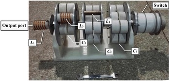
Fig. 11. Experimental setup of the three-section anti-resonance pulse forming network.
The operating process of the generation is as follows: firstly, Capacitor C 1 was charged by the pulse transformer with negative pulse, and we can control the charging voltage through the trigger system of the gas spark gap switch. After the gas spark gap switch closed by an external trigger pulse voltage, Capacitor C 1 discharged to the parallel resonance network of L 2 and C 2. Through the shaping effect of L 2 and C 2, a quasi-square pulse could be delivered by a resistive load of 50 Ω.The output voltage signals were measured by a 2000:1 resistive voltage divider, which could respond well to ns-range pulses. Then the voltage signal from the divider was viewed and recorded on a LeCroy 44MXs-B digitizing oscilloscope.
3.2. Experimental results of two-section network
For the two-section network, just remove the capacitor C 3 and inductor L 3 in Figure 9, and change the capacitance of capacitors C 1, C 2 and inductance of inductors L 1, L 2 by Eq. (15). It is much easier to obtain ideal output pulse for it merely has two inductors needed to be adjusted comparing with three-section network's three inductors. The simulation results and experimental results of the two-section network are shown in Figure 12.

Fig. 12. Simulation and experimental waveforms of the output pulses of two-section network.
It is obviously shown that the pulse width of the output pulse was about 400 ns with the rise time about 90 ns, the flat top up to 180 ns and the fall time about 217 ns. The experimental results were consistent with the simulation results.
3.3. Experimental results of three-section network
The study of three-section anti-resonance network was carried out due to inefficiency of two-section network. As for the three-section network, researches on the effect of L 1, L 2, and L 3 on the output pulse must be carried out to obtain ideal output pulse as each of the three inductors have great impact on the pulse shape.
At first, experiments on the effect of inductor L 1 on the output pulse is carried out when L 2 is about 150 nH and L 3 is about 1.0 µH. The simulation results and experimental results are shown in Figure 13.

Fig. 13. Effect of L 1 on the output pulse. (a) Experimental results; (b) Simulation results.
As shown in Figure 13, the experimental results are consistent with the simulation results. When the value of L 1 is smaller than expected, overshoots occurs at the beginning of the output pulse. On the contrary, rise time will be very long till the flat top of the pulse is exhausted. The results can perfectly explain why the modifications of inductors can eliminate the overshoots.
Then, experiments on the effect of inductor L 2 on the output pulse is carried out when L 1 is about 2.5 µH and L 3 is about 1.0 µH. The simulation results and experimental results are shown in Figure 14. It is difficult to adjust the value of L 2 to be accuracy for it is supposed to be extremely small. A little change of the value of L 2 will lead to oscillations of the output pulse as is shown in Figure 14.

Fig. 14. Effect of L 2 on the output pulse. (a) Experimental results; (b) Simulation results.
Finally, experiments on the effect of inductor L 3 on the output pulse is carried out when L 1 is about 2.5 µH and L 2 is about 150 nH. The simulation results and experimental results are shown in Figure 15.

Fig. 15. Effect of L 3 on the output pulse. (a) Experimental results; (b) Simulation results.
As shown in Figure 15, smaller value of L 3 could short the pulse width and down the flat top of the pulse while bigger value of L 3 got the contrary results.
In conclusion, the rising edge of the pulse is influenced mostly by L 1, while L 1, L 2 have larger impact on the flat top and the falling edge.
According to the results shown above, it is not difficult to obtain ideal pulses by adjusting the inductance of the three inductors. The preliminary result of the three-section network is shown in Figure 16.

Fig. 16. Simulation and experimental waveforms of the output pulses of three-section network.
Obviously, the pulse width of the output pulse was about 400 ns with the rise time about 60 ns and the flat top up to 240 ns, which was consistent with the simulation results. The Experimental results of two- and three-section networks are shown in Figure 17.

Fig. 17. Comparison of experimental waveforms of the output pulses between two- and three-section anti-resonance networks.
More details about the improvements of three-section anti-resonance network over two-section anti-resonance network are shown in Table 1.
Table 1. Typical parameters of the output pulse of two- and three-section network with pulse width 400 ns

Experimental results, which are consistent with the simulation results, show that the improvements of the three-section over the two-section network is conspicuous for the flat top of the output pulse, increasing from 180 to 240 ns, the rise time, decreasing from 90 to 60 ns and the fall time, decreasing from 217 to 109 ns.
4. APPLICATION IN THE MARX GENERATOR
In this paper, an anti-resonance PFN has been designed, analyzed, and tested for its application in generating quasi-square pulse. As it is known, the Marx generator is one of the most important kinds of high-power pulse generators. However, single Marx generators could only output damped sine pulse. Thus, the PFN-Marx is a proposed structure to generate high-voltage quasi-square pulse. Since a Marx generator could be regarded as one-section LC series resonance network, part of an anti-resonance PFN, when it is discharging, its output pulses could be shaped into quasi-square pulses through the network. A simple experiment based on the two-section anti-resonance network was carried out to demonstrate the feasibility of this idea.
To prove that anti-resonance networks could also generate pulses with pulse width about 100 ns, the requirement of τ = 100 ns, ρ = 40 Ω is accepted and parameters of two-section network can be obtained from Eq. (9) as follows:
 $$\left\{ {\matrix{ {C_1 = 1.05\,{\rm nF},} & {L_1 = 1.23\,{\rm \mu H,}} \cr {C_2 = 0.79\,{\rm nF},} & {L_2 = 228\,{\rm nH}{\rm.}} \cr}} \right.$$
Since the capacitors of the Marx generator are the same and connected in series when discharging, the capacitance of the capacitors of four-stage Marx generators should be 4.2 nF. As shown in Figure 18, the four-stage Marx generator with the pulse shaping network was designed according to the two-section anti-resonance network shown in Figure 2. The four-stage Marx generator mainly consisted of four capacitors C 11, C 12, C 13, C 14, and four gas gap switches U 1, U 2, U 3, U 4. The charging inductances and isolating inductances were the same named as L M. All capacitors except C 2 were charged by the pulse transformer with negative pulse.

Fig. 18. PSpice circuit of a four-stage Marx generator with the pulse shaping network.
The operation of the system was as follows: at first, the primary switches of the pulse transformers were closed, and the primary capacitors in the transformer discharged to the four-stage Marx generator. When the charging voltage on the capacitor C 11 was greater than the voltage that switch U 1 could withstand, the gap broke down and the voltage at point A became zero. As the voltage on a capacitor could not change abruptly, the voltage at point B became U 0; therefore, the voltage across switch U 2 became 2U 0. If the breakdown voltage on U 2 was set between U 0 and 2U 0, the gas gap could be broken down. The breakdown of the subsequent switches was similar to the aforementioned case. After all the gas gap switches were closed, the four-Marx generator began to discharge through the shaping network, parallel resonance network composed of L 2 and C 2. The output voltage on the resistive load of 50 Ω would be a quasi-square pulse. The equivalent experiment setup was carried out as shown in Figure 19.

Fig. 19. Experiment setup of a four-stage Marx generator with the pulse shaping network.
The performance of four-stage Marx generator shaped before and after was tested by experiments. The experimental results were shown in Figure 20. The simulation and experimental results of the pulse shaping network of the four-stage Marx generator is shown in Figure 21. According to Figure 20, a sine pulse generated by the four-stage Marx generator is able to be shaped into a quasi-square pulse using anti-resonance network. It is shown that the pulse width of the output quasi-square pulse was about 110 ns, a little more than expected, and the voltage amplitude could be calculated as 11.8 kV. As shown in Figure 21, the experimental result was consistent with the simulation result, where the pulse width was calculated as about 100 ns.

Fig. 20. Experimental results of a four-stage Marx generator before and after adding the shaping network.

Fig. 21. Simulation and experimental results of a four-stage Marx generator with the pulse shaping network.
5. CONCLUSIONS
The compactness and miniaturization properties are of great importance for quasi-square pulse generators. In this paper, theoretical and experimental research of two- and three-section anti-resonance networks, which can generate quasi-square pulse are carried out and it was found that the improvements of the three-section over the two-section network are conspicuous. A compact quasi-square pulse generator based on these two kinds of networks is designed in this paper with the requirement of pulse width τ = 400 ns. Preliminary experiments were carried out and the experimental results were consistent with the simulation results. As for the three-section network, the flat top of the output pulse is about 240 ns, while the rise time is <60 ns and the fall time is about 109 ns comparing with the two-section network's 180, 90, and 217 ns, respectively.
The application of the anti-resonance network in the Marx generator is put forward and demonstrated in this paper. A two-section anti-resonance network based on the four-stage Marx generator was designed and constructed. The output voltage on the resistive load of 50 Ω was 11.8 kV with a pulse width of 110 ns.
ACKNOWLEDGEMENTS
The authors wish to thank X. Yang, Y. Z. Shao and X. Zhou for their suggestions and encouragements to the experiment. The assistance of M. Zhu in the experiment is also grateful acknowledged.


