1. INTRODUCTION
Use of the linear pulse transformer, where a primary coil is powered directly from the capacitive storage, and the secondary coil with vacuum isolation is a perspective and actively developed technology of high power electron accelerators (Bastrikov et al., Reference Bastrikov, Vizir, Volkov, Durakov, Efremov, Zorin, Kim, Kovalchuk, Kumpyak, Loginov, Sinebryukhov, Tsou, Chervyakov, Yakovlev and Mesyats2003; Kim et al., Reference Kim, Bastrikov, Kovalchuk, Volkov, Durakov, Kumpjak, Sinebryukhov and Tsou2005). Such accelerators allow obtaining voltage pulses of 105–106 V with rise time of ~100 ns in vacuum diodes with a resistance of 1–10 Ohm (Kim et al., Reference Kim, Bastrikov, Volkov, Durakov, Kovalchuk and Sinebryukhov2003; Mazarakis et al., Reference Mazarakis, Fowler, McDaniel, Olson, Rogowski, Sharpe, Struve, Stygar, Kim, Sinebryukhov, Gilgenbach and Gomez2007). The accelerator parameters can be improved with the use of a plasma-filled diode.
Plasma-filled diodes have been employed in the pulsed power technique as high-current, relativistic electron-beam sources (Miller et al., Reference Miller, Poukey and Wright1975; Weber et al., Reference Weber, Boller, Cooperstein, Kellogg, Stephanakis and Swanekamp1993). These diodes can be used as a powerful pulsed radiation sources for some applications such as X-ray radiography (Weber et al., Reference Weber, Allen, Commisso, Cooperstein, Hinshelwood, Mosher, Murphy, Ottinger, Phipps, Schumer, Stephanakis, Swanekamp, Threadgold, Biddle, Clough, Jones, Sinclair, Swatton, Carden and Oliver2008) and radiation effects testing (Weber et al., Reference Weber, Hinshelwood, Murphy, Stephanakis and Harper-Slaboszewicz2004). E-beam formation in the diode gap preliminary filled with plasma occurs after a stage of high-current discharge with resistance much less than a wave impedance of the feeding generator (hereafter referred to as “low-resistance phase”). The discharge current of low-resistance phase provides magnetic self-insulation of vacuum line of transformer secondary coil (Bailey et al., Reference Bailey, Creedon, Ecker and Helava1983). The phase of e-beam formation is characterized by fast rise of resistance (hereafter referred to as “high-resistance phase”). In this phase, the diode can act like an opening switch that results in increase of output power of the accelerator (Meger et al., Reference Meger, Comisso, Cooperstein and Goldstein1983; Abdullin et al., Reference Abdullin, Bazhenov, Bastrikov, Bugaev, Kim, Kovalchuk, Kokshenev, Mesyats and Suchushin1985). Thus, the problem of diode resistance matching with a low wave impedance of the transformer (as a rule of <10 Ohm) can be solved due to partial or complete energy transfer from the primary capacity storage into the circuit inductance during the low-resistance phase.
An e-beam in the plasma-filled diode gap is charge neutralized and that promotes its compression exerted by self magnetic field (Suladze et al., Reference Suladze, Tskhadaya and Plyutto1969). The problem of large-area beam formation and transport without external guiding magnetic field, preventing a beam self-focusing, requires studying.
Plasma-filled diodes with current of ≈100 kА at duration of low-resistance phase of ≈100 ns were investigated in the present study both for generation of focused and wide-aperture e-beams.
2. EXPERIMENTAL DESIGN
Experiments were fulfilled with use of the pulsed linear transformer (Zherlitsyn et al., Reference Zherlitsyn, Kovalchuk, Smorudov, Tsoy, Visir and Zorin2008). The following transformer output parameters have been obtained at operation with a quasi-stationary low-resistance load (in the form of the cylindrical electronic diode, operating in the self-magnetic insulation mode): the current amplitude is 110 kA, the current rise time is 115 ns, the voltage amplitude is 370 kV, the peak power is 40 GW (Belomyttsev et al., Reference Belomyttsev, Grishkov, Zherlitsyn and Kovalchuk2009).
Two configurations of a plasma-filled diode were investigated: the first one for generation of focused (Fig. 1a) and the second one for wide-aperture (Fig. 1b) e-beams.

Fig. 1. Design of two variants of plasma-filled diode. 1 – plasma gun; 2 – cathode; 3 plasma channel; 4 – anode; 5 – metal foil; 6 – collector.
In the first variant of the diode (Fig. 1a) plasma is formed by one plasma gun (1) of capillary type with dielectric surface discharge. The gun is located on a potential central electrode. Plasma is injected across the anode-cathode gap through a stainless steel tube with diameter of 12 mm (2). This tube forms a plasma channel (3) with small radial size in order to get high linear current density on the cathode. Distance between the tube end (2) and the anode (4) is equal to 30 mm. Distance from the end surface of plasma gun to the anode is equal to 50 mm.
In the second variant (Fig. 1b), the diode is divided into separate sections for increasing in cross-sectional area of a generated beam and reducing of a current density at the anode. Sectioning is made in such a way that the magnetic field in each section is defined only by it's own current, instead of a diode total current. For this purpose, the anode of the diode (4) has been divided into four or six cylindrical cavities with diameter D. Centers of anode cavities are placed at a diameter of 80 mm. Plasma guns (1) are located in cathode tubes (2) from stainless steel with diameter of 12 mm and length of 110 mm. Each tube is dipped in the anode cavity at a depth of 30 mm. Gap between end of cathode tubes and the anode plane is equal to 30 mm.
Diode current rise rate dI d/dt was measured by the calibrated inductive probe. The diode current I d is calculated from the probe signal. The Rogowski coil I r, installed on an edge anode flange, was also used for monitoring of current. In the first variant, the Rogowski coil measures all diode current terminated at the anode. In the second variant, the coil measures the electron current behind the metal foil (5). Coil registrations were supplemented by current measurements in the collector circuit (6) I sh by means of the resistive shunt. Output voltage of each stage U 1–U 6 and current rise rate in the beginning of a transformer coaxial line dI 0/dt were also registered in the experiments. Measured signals were used for calculation of: (1) voltage across the diode  , where L — inductance of a vacuum coaxial before the diode cathode; (2) diode resistances
 ![]() ; (3) load power P d = U dI d; (4) the energy transferred into the diode W d = ∫ P ddt.
; (3) load power P d = U dI d; (4) the energy transferred into the diode W d = ∫ P ddt.
Plasma guns were powered from a capacitor block with a capacity of 80 nF at a charge voltage of 80 kV (Zherlitsyn et al., Reference Zherlitsyn, Kovalchuk and Smorudov2009). Amplitude of discharge current in the first half wave at operation on one plasma gun is 9.5 kА, current rise time is 450 ns. At operation with 4 or 6 plasma channels, the current amplitude in each gun was 2 kА and 1.6 kА, respectively. Plasma parameters in the diode were varied by change of time delay t d between the plasma guns and transformer firings.
3. EXPERIMENTAL RESULTS
Experiments with plasma-filled diode were carried out at 90 kV charging voltage on the transformer stages. Vacuum volume was pumped out by turbo-molecular pump until residual pressure is lower than 5 × 10⁻⁵ Torr. Inductance of the transformer vacuum line was 330 nH in these experiments. The short circuit current in a transformer contour is 160 kА with rise time of 240 ns. In experiments with plasma-filled diodes, maximum values of output voltage and power are realized at duration of low-resistance phase of 100–120 ns that corresponds to diode current of 90–110 kА.
Figure 2 shows experimental results for low-resistance phase of 100–120 ns in the form of diode voltage plotted versus current in the single plasma channel (section). The data for the sectioned diode are calculated on the assumption of equal current division between sections. The largest current density and generated voltage are realized at operation of the diode with one plasma channel. With current reduction through the plasma channel from 100 to 15 kА the diode voltage amplitude has decreased from U d ≈ 1 MV to 400 kV.

Fig. 2. Diode voltage amplitude U d as a function of current in single plasma channel I 1.
Regimes of the e-beam generation are described below for diodes with 1, 4, and 6 plasma channels.
3.1. Plasma-Filled Diode with One Plasma Channel
Operation regime with one plasma channel is shown in Figure 3. Peak value of current in the plasma channel I d ≈ 100 kА is realized, when time delay is t d = 2.8 µs. The voltage U d ≈ 1 MV with front T f ≈ 15 ns is generated on the diode. The diode power is P d ≈ 100 GW. The resistance of plasma channel R d reaches 12 Ohm. The load energy W d ≈ 4 kJ is transferred to the diode within 200 ns and 50% of the dissipated energy (2 kJ) in the diode is released during the first 30 ns. Note that the currents measured in the beginning of a vacuum coaxial line of the transformer and before the diode coincide. It shows that leakages in a vacuum line current are negligible and all current flows in the diode. The lifetime of the cathode with plasma gun is determined by the destruction of the plasma gun capillary. In our experiments, the lifetime of the capillary was several dozens shots.

Fig. 3. Transformer discharge on plasma-filled diode with one plasma channel.
Figure 4 shows the beam imprint on e-beam-sensitive plastic behind a Ti foil with the thickness of 50 µm. The stainless steel mask with thickness of 1.5 mm was installed just before the foil. Holes with a diameter of 1.8 mm and step of 4 mm are made in the mask. The mask transparency is about 15%. The mask decreases intensity of the electron flow on e-beam-sensitive plastic and prevented ablation of the Ti foil into vacuum coaxial of the transformer. The external boundary of an imprint has diameter of 40 mm. The area of maximum intensity of darkening is located on beam center with a diameter of 20 mm. Form of the imprint shows the e-beam focusing by self magnetic field. Provided that main part of current flows in the circle with diameter of 20 mm, one can estimate the current density on the anode and specific power as 30 kА/cm2 and 30 GW/cm2, respectively.

Fig. 4. Beam imprint in the diode with one plasma channel.
3.2. Plasma-Filled Diode with Four Sections
The next series of experiments has been done with the plasma-filled diode with four isolated plasma channels (Fig. 1b). Initial diameter of anode cavities was D = 50 mm. Oscilloscope traces and calculated curves (current I d, voltage U d, and diode resistances R d) for this case are shown in Figure 5 (curves 1). At time delay t d = 1.3 µs amplitude of the diode current is I d ≈ 92 kА that corresponds to current of 23 kА in one section. The diode resistance rises up to level of 6 Ω (one section resistance of 24Ω) and the voltage U d ≈ 500 kV is generated on the diode. The load energy is W d ≈ 4.8 kJ, the peak power is P d ≈ 43 GW.

Fig. 5. Transformer discharge on plasma-filled diode with four sections. Diameter of anode cavities of 50 mm (curves 1), 37 mm (curves 2), and 28 mm (curves 3).
Number of sections in the diode and homogeneity of a generated beam is defined by diameter of anode cavities D. Experiments have been provided in order to estimate minimum diameter D, which doesn't lead to a significant deterioration of pulse parameters. Experimental results for anode cavities with diameters D = 37 and 28 mm are given in Figure 5 (curves 2 and 3). At the fixed time delay t d the current amplitude in the diode has not changed. Decrease of diameter to D = 37 mm results in a small decrease of the diode voltage amplitude and peak power (480 kV and 40 GW). Dissipated energy in channel was not changed. Decrease of diameter to D = 28 mm results in a significant drop in the diode resistance, diode voltage and diode energy (4Ω, 370 kV, and 4.1 kJ, respectively).
Optimal diameter D has been defined as approximately 37 mm on base of these experiments. Sections with this diameter were used in experiments with six parallel plasma channels.
3.3. Plasma-Filled Diode with Six Sections
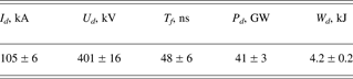
Figure 6 shows oscilloscope traces and calculated curves, demonstrating operation of the linear transformer on plasma-filled diode with six sections. The current amplitude in the diode is I d ≈ 105 kА (current per section is 17.5 kА), the diode voltage is U d ≈ 410 kV, and the output power is P d ≈ 44 GW. Rise time of the voltage pulse is T f ≈ 50 ns. Full duration of the voltage pulse is 250 ns. The diode resistance R d rises to 4Ω. The diode energy is W d ≈ 4.2 kJ, which corresponds to 54% efficiency in comparison with the energy stored in the stages capacitors. Electron current I r ≈ 70 kА with rise time of 30 ns were measured behind a Ti foil with a thickness of 50 µm. Waveform of the current I r correlates with the diode voltage shape.

Fig. 6. Transformer discharge on plasma-filled diode with six sections.
The main parameters of a pulse in the diode are summarized in Table 1. Table 1 presents average values <x> of the pulse parameters in a series from 12 shots and root mean square deviation σ for these parameters. One can see that pulse parameters are well reproducible, namely: deviation σ for voltage is equal to 16 kV (4% from average value), the deviation for the power is about 7%.
Table 1. Average values of parameters of 12 pulses and an root mean square deviation of parameters from average value 〈x〉 ± σ.

The imprints of a beam, generated in the sectioned diode, are presented in Figure 7. Imprints are made on e-beam-sensitive plastic located behind a Ti foil with a thickness of 50 µm and distances of 10, 20, and 27 mm in three different shots. A metal grid with a transparency of 65% was placed before the foil. E-beams autographs of each of six sections looks almost like identical circles with diameter of ≈30 mm at a distance of 10 mm behind a foil (Fig. 7a). This imprint shows that the generator current is equally divided between sections. Centers of the beams imprints of separate sections are located at a diameter of 70 mm. This diameter is slightly less than the diameter of plasma guns placement (80 mm). Nevertheless, we can make the conclusion that current is distributed uniformly over the surface of cathode tubes. When distance from the foil to the autograph film increases to 20 mm (Fig. 7b) e-beams traces of near sections are “washed” and the imprint takes the form of a ring. External diameter of a ring of 80 mm shows that there is some beam compression in the drift region behind a foil. At further increase in distance to 27 mm (Fig. 7c) the imprint evolves in a circle in area S ≈ 50 cm2. An estimated average current density is 1 kА/cm2 in e-beam on distance of 27 mm behind a foil.
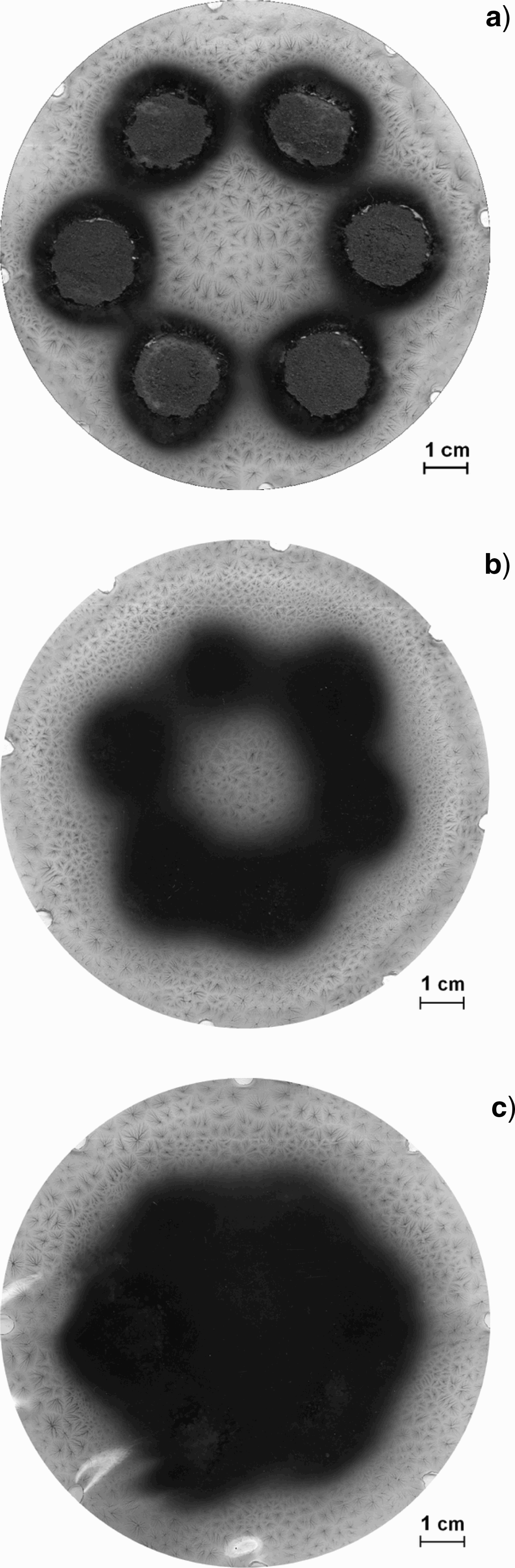
Fig. 7. Beam imprints in plasma-filled diode with six sections on distances of 10 (a), 20 (b), and 27 (c) mm behind an anode foil.
4. SYNCHRONIZATION OF SECTIONS IN PLASMA-FILLED DIODE
It is necessary to provide synchronous beginning of high-resistance phase of all sections for production of homogeneous wide-aperture e-beam at use of sectioned plasma-filled diode. It is possible to provide synchronization of sections due to electric coupling: premature resistance growth in one or several plasma channels will lead to current increase in the others that in turn will provoke their transition into a high-resistance phase.
The qualitative analysis of a transient process in a plasma-filled diode can be made for the case when part of the sections has passed into a high-resistance phase, using the electrical circuit in Figure 8. Here L 1 is the inductance of the transformer upstream of a plasma-filled diode; L 2 is an equivalent inductance of short-circuited sections; L 3 is an equivalent inductance of sections, where the resistance R 3(t) starts to grow. Circuit parameters in our experiments: transformer inductance is L 1 ≈ 430 nH, inductance of one diode section is L p ≈ 15 nH. In practice, the sections have to be synchronized in front of the diode voltage spike. Resistance of individual section at the pulse front can be approximated by linearly rising function with a rise rate of k ≈ 0.5 Ω/ns (oscillograms in Figs. 3, 5, and 6).

Fig. 8. Electric equivalent circuit for the analysis of sections synchronization in the plasma-filled diode.
Assumed that at instant t 0 = 0 current I 0 flows in the inductance L 1, the equivalent resistance of several sections starts to increase under the law R 3(t) = k 3 × t, and the rest of sections remain short-circuited, then equation for a current in short-circuited sections will look like:

where ![]() current in L 2 at instant t 0 = 0;
current in L 2 at instant t 0 = 0; ![]() .
.
Analysis of Eq. (1) shows that the most unfavorable case for synchronization is the premature transition into a high-resistance phase of one section. Dependence of the normalized current in short-circuited sections on time I 2(t)/I 2(0) for this case is shown in Figure 9. Calculation was performed for variants of the diode with sections number of N = 4, 6, 8, 10, and 12. Current rise time in short-circuited sections is ≈15 ns, which is several times less than the voltage front. At total number of sections N ≤ 10 the maximum possible increase of current in short-circuited sections exceeds 10%.

Fig. 9. Current change in short-circuited sections I 2(t)/I 2(0) in case of one section transition into a high-resistance phase. Total number of sections in the diode is N = 4, 6, 8, 10, and 12.
The simple estimation of current-rise time in L 2 can be derived also by taking into account that L 1 ≫ L 2 and L 1 ≫ L 3. The time moment, when the second item on right-side of the Eq. (1) will decrease 10 times, can be written as  . At this time the relative increase of a current will be ≈(1 + L 2/L 3).
We can make the conclusion that the resistance rise rate of the plasma channel of 0.5 Ω/ns, realized in the experiments, will result in the current increase more than 10% during ≈15 ns in the remained short-circuited sections at total number of sections of ≤10. This increase of current should force transfer of the remained short-circuited sections into a high-resistance phase, providing automatically synchronization of the sections transition, despite on initial spread in plasma parameters in the sections,. Finally we can mention, that in experiments with plasma-filled diode, the significant time spread in sections operation was not observed.
5. CONCLUSION
Experimental results have proven realization of a powerful electron source on the base of a linear transformer and plasma-filled diode.
Maximum output voltage and power are obtained at using of one plasma channel of small diameter with high linear current density in the diode. At use of the plasma channel with diameter of 10 mm, the diode voltage of 1 MV with front of 15 ns was obtained at current of 100 kА. Energy of 4 kJ with peak power of 100 GW is transferred into the e-beam.
Possibility of use in the diode of isolated parallel plasma channels of small diameter is shown for e-beam generation with cross-sectional area of ≥50 cm2. With use in the diode of six plasma channels the voltage of 400 kV with front of 50 ns is realized at the current of 100 kА. Diode energy in this case is 4.2 kJ with peak power of 40 GW.
In experiments with plasma-filled diodes the energy transmission efficiency into an e-beam was 52–54% compared to the primary storage energy.