1. INTRODUCTION
The generators of large-section (S > 10 cm2), high-current (10–30 kA) relativistic pulsed electron beams of moderate power density (107–109 W/cm2) stimulate considerable interest in many applications, such as the production of high-power X radiation pulses (Liu et al., Reference Liu, Zou, Wang, Zeng and He2008; Wong et al., Reference Wong, Woo and Yap2007; Stein et al., Reference Stein, Fill, Habs, Pretzler and Witte2004; Kasperczuk et al., Reference Kasperczuk, Pisarczyk, Nicolai, Stenz, Tikhonchuk, Kalal, Ullschmied, Krousky, Masek, Pfeifer, Rohlena, Skala, Klir, Kravarik, Kubes and Pisarczyk2009; Hong et al., Reference Hong, He, Wen, Du, Teng, Qing, Huang, Huang, Liu, Wang, Huang, Zhu, Ding and Peng2009), microwave sources (Li et al., Reference Li, Men, Liu and Wen2007, Reference Li, Yuan, Zhang, Shu and Zhang2008a, Reference Li, Liu, Wen and Liu2009c), and physics of high energy densities in matter (Zou et al., Reference Zou, Liu, Zeng, Han, Yuan, Wang and Zhnag2006; Zhou et al., Reference Zhou, Yu and He2007; Clardi et al., Reference Clardi, Lebedev, Chittenden and Bland2002), particularly as candidates for surface modification of various materials (Chen et al., Reference Chen, Unick, Vafaei-Najafabadi, Tsui, Fedosejevs, Naseri, Masson-Laborde and Rozmus2008; Ozur et al., Reference Ozur, Proskurovsky, Rotshtein and Markov2003; Tahir et al., Reference Tahir, Kim, Matvechev, Ostrik, Shutov, Lomonosov, Piriz, Cela and Hoffmann2008, Reference Tahir, Matveichev, Kim, Ostrik, Shutov, Sultanov, Lomonosov, Piriz and Hoffmann2009). Research on surface modification of materials by electron-beam radiation, together with the investigation of basic principles of interaction between electron beam and surface, is constantly growing. In most of the cases, surface modification is characterized by visual changes like cracks, ripples, spikes, etc., when the material undergoes structural modification. It is important to understand the processes involved, at low and high levels of impact, ranging from texturing to ablation, and accompanying processes, as well as interactions with the plasma formed on the target surface. However, until recently the phenomena, occurring on the interaction of pulsed electron beams of moderate power density with metals, are far from being solved completely.
The electron guns with an anode and an explosive-emission cathode are the most appropriate systems for the production of high-current pulsed electron beams (Li et al., Reference Li, Liu, Xu, Wen and Liu2008c, Reference Li, Liu, Xu, Chen, Chang, Wan and Wen2009e; Tarasenko et al., Reference Tarasenko, Baksht, Burachenko, Kostyrya, Lomaev and Rybka2008). The beam power is mainly limited by pulsed power technology (Liu et al., Reference Liu, Cheng, Qian, Ge, Zhang and Wang2009; Zou et al., Reference Zou, Liu, Zeng, Han, Yuan, Wang and Zhnag2006; Chuvatin et al., Reference Chuvatin, Kokshenev, Aranchuk, Huet, Kurmaev and Fursov2006; Yatsui et al., Reference Yatsui, Shimiya, Masugata, Shigeta and Shibata2005). The appearance of advanced high-energy technologies provides the possibility of obtaining accelerated plasma jets from vacuum arc discharge sources, which are developed in vapor of the cathode materials under the application of high accelerating pulsed voltage. The electric field is localized within the cathode layer of ion space charge, whose thickness is generally much less than the anode-cathode (A-K) gap (Tarasenko et al., Reference Tarasenko, Shunailov, Shpak and Kostyrya2005). Once the electric field of microprotrusion on the cathode surface exceeds the threshold value, the explosive electron emission is initiated on the cathode, leading to the formation of dense plasma spots. Indeed the emission center in this discharge is a plasma spot with small dimensions (10−3–10−6 m), large velocity of motion toward (up to 104 m/s), and high temperature (significantly exceeding the boiling temperature of the cathode material) (Krasik et al., Reference Krasik, Dunaevsky, Krokhmal, Felsteiner, Gunin, Pegel and Korovin2001). Owing to the high temperature, the material in the cathode spot is subjected to the intense decomposition and sputtering. Electron-beam treatment is performed on a specially designed electron beam setup based on a high-current relativistic electron beam source. The further development of electron beam sources is associated with widening the ranges of the beam parameters, that is, increasing the efficiency of conversion of the energy stored in the high-voltage pulse generator to the beam energy, lengthening the lifetime of the cathode, and, first of all, increasing the pulse duration. The electron beam source, in view of the large cross section of the beam and the high productivity of the electron-beam setup, can be considered a basis for the development of a new technology for surface treatment. Nanosecond laser pulses are widely used for surface treatment (Beilis, Reference Beilis2007; Chaurasia et al., Reference Chaurasia, Munda, Ayyub, Kulkarni, Gupta and Dhareshwar2008; Latif et al., Reference Latif, Anwar, Aleem, Rafique and Khaleeq-Ur-Rahman2009; Mirdan et al., Reference Mirdan, Jawad, Batani, Conte, Desai and Jafer2009; Trtica et al., Reference Trtica, Radak, Gakovic, Milovanovic, Batani and Desai2009). However, the method of nanosecond laser is suitable only for the investigation of microstructure evolution, mainly due to the comparatively small thickness of the alloyed layer, the small cross-sectional area, the high reflection, and the low efficiency. The pulsed melting, in the case of the electron-beam treatment, makes it possible to dissolve second phase particles and produce highly concentrated surface alloys.
Recently, several high-current relativistic electron-beam sources have emerged as providing high current density emission from cathodes with mechanically and thermally robust construction (Shiffler et al., Reference Shiffler, Haworth, Cartwright, Umstattd, Ruebush, Heidger, Lacour, Golby, Sullivan, Duselis and Luginsland2008a, Reference Shiffler, Heidger, Cartwright, Vaia, Liptak, Price, Lacour and Golby2008b; Vekselman et al., Reference Vekselman, Gleizer, Yarmolich, Felsteiner, Krasik, Liu and Bernshtam2008; Li et al., Reference Li, Liu, Wen, Men and Liu2008b). The related research has focused on the generation, control, transport, and concentration of electron beams. However, the discussions on the interaction physics of high-current pulsed electron beam with anode surface are scanty in previous publications. In this paper, the characteristics and mechanisms for the changes in the microstructure and properties of the surface layers of an anode irradiated by high-current pulsed electron beam are discussed.
2. PULSED POWER SYSTEM
The experimental system consists of an initial energy supplier (capacitance bank), a trigger switch, a transformer with a coupling coefficient of 0.89, an electrically exploded opening switch (EEOS), a sharpening spark-gap switch as main switch, and a high-current electron beam diode as load (see Fig. 1). When the charged capacitance bank has a 45 kV voltage, the voltage across the trigger switch is up to 55 kV. Then a negative high-voltage pulse is loaded on the trigger electrode, and the breakdown between the trigger and input electrodes occurs due to the significant electric field enhancement. This is accompanied by the secondary discharge between the trigger and output electrodes. Thus the trigger switch rapidly turns on, and the capacitance bank discharges, forming a pulsed high current in the primary circuit of the transformer. Meanwhile, the EEOS delivers a pulsed high current in the branch circuit of the secondary side of the transformer. The EEOS consisted of an organic glass plate, macromolecule rods (polytetrafluor ethylene), and two arrays of Cu wires arranged in a “Z” shape. These wires were positioned at the two sides of the plate, each side having eight wires. Each wire was 0.06 mm in diameter and 770 mm in length. The plate was placed in a cylindrical chamber made of macromolecule, 20 cm in diameter and 50 cm in length. This chamber was filled with 4 atm. SF6 or N2 that acts to inhibit arcing. Once the pulsed high current passes the EEOS, the electrical wire explosion occurs as the temperature grows fast due to Joule heating. That is, the EEOS turns off, and an over 400 kV voltage forms across the main switch, leading to the self-breakdown and further sharpening the accelerating pulse. This provides a sufficiently strong electric field to the cathode to emit the high-current electron beam. A Rogowski coil was used to measure the beam current I b, and the diode voltage ϕac was monitored by a resistive divider. The voltage or current signal was transmitted through a coaxial cable to a Tek 3052B oscilloscope (sampling rate of 5Gs/s).

Fig. 1. (Color online) Diagram of a high-current electron-beam accelerator with inductive energy storage. The accelerator consists of the initial energy source, EEOS, coaxial transformer, main switch, and vacuum diode. The vacuum vessel shows the cathode mount, cathode, anode, and vacuum pump. The A-K gap can be changed by moving the shaft upon which the cathode is mounted.
The chamber of the diode represents a cylinder with a diameter of 35 cm and a length of 40 cm. The vacuum vessel operated at <5 × 10⁻⁵ torr and was evacuated by a turbo pump with a pump rate of ~300 l/s. A Cu plate, 21 cm diameter and 0.6 mm thickness, was used as an anode. The diode gap d ac was in the range of (1–7) cm. The tested cathode was based on a carbon fiber. This cathode consisted of discrete needles. Further, the emitting surface of each cathode was planar, namely, the needles on the cathode surface had the same length. Here, each fiber needle was 5 mm high, with a 1.5 mm diameter, and spaced by 9 mm. Each needle was composed of thousands of carbon fibers with 2.5 µm radius. The anode surface was characterized by various analytical techniques, before and after electron-beam irradiation. Surface morphology was investigated by scanning electron microscopy (SEM). The SEM was coupled to an energy dispersive spectroscopy analyzer (EDS) for determining elemental surface compositions.
3. RESULTS AND DISCUSSIONS
3.1. Structure of the Anode Surface
The typical waveforms of diode voltage ϕac and beam current I b at d ac = 19 mm are shown in Figure 2a for the carbon fiber cathode of r c = 30 mm radius. The voltage amplitude was ~350 kV and the voltage pulse width was ~300 ns. The diode voltage rapidly increased up to 300 kV within 20 ns. Additionally, it was seen that, from the waveform of the diode current, the maximum emission current was ~4.5 kA and its rise-time was ~130 ns. Then the maximum electric field was kept at a level of 170 ± 10 kV/cm. Further, it is reasonable that the current slower dropped relative to the decrease in the voltage pulse, due to the usage of inductive energy accumulators. Slightly, different accelerating voltage and current were observed in experiment tests. Figure 2b presents the beam power and energy density on the anode target. Here, it is assumed that the beam radius on the anode surface is equal to the cathode radius, namely, r b = 30 mm. One can see that the peak beam power reached ~1.5 GW. By integrating the power, ~13 J/cm2 energy density was obtained.

Fig. 2. (Color online) (a) Waveforms of the accelerating voltage ϕac and the beam current I b, and (b) beam power and energy deposition. The diode gap is d ac = 19 mm.
Figure 3 presents the microscopic surface morphology of the Cu target after electron-beam irradiation. It can be seen that, from Figure 3a, many craters with 0.5–1 µm diameter appeared on the target surface. Here, the observed area is located at the center of beam cross-section. In Figure 3b, which is at the edge of beam, it was found that the craters had a smaller depth compared with the center. Additionally, Figures 3c and 3d, respectively, show the EDS analysis before and after electron-beam irradiation. Surprisingly, the carbon content on the Cu target increased significantly by electron-beam irradiation, with the percent of atom number from 23.83% to 51.15% (see Table 1). It clearly indicates the carbon deposition on the Cu target irradiated by electron beam from carbon fiber cathode. Also, this is likely due to the sputtering of cathode materials under explosive electron emission.

Fig. 3. (a) and (b) Typical SEM images of surface morphology on Cu target after electron-beam irradiation, and the EDS images before (c) and after (d) electron-beam irradiation.
Table 1. Elemental surface compositions on target surface by EDS analysis before and after electron-beam irradiation
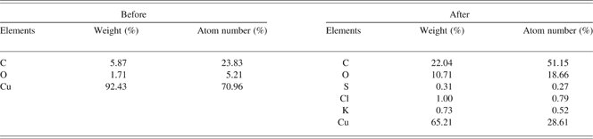
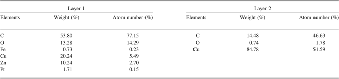
Figure 4a shows the oblique-view SEM image of target surface after electron-beam irradiation. It was found that the formation of microcraters is followed by the appearance of the melt zone with solidified liquid-metal jets radiated outward. This testifies to the intense vaporization of the anode material. Liquid metal is ejected from the crater under the action of the vapor pressure. The cross-section SEM image of Cu target is shown in Figure 4b. Interestingly, the layer structure on the cross section appeared. In Figure 4b, layer 1 is a uniformly distributed, fine-structured surface layer with ~20 µm thickness. The subsurface, layer 2, is characterized by a cellular structure consisting of cells with the typical size of <3 µm. Further, these cells have a larger vertical dimension. Most notably, there is a large difference in the carbon content between layers 1 and 2, from 77.15% to 46.63% (see Table 2).

Fig. 4. (a) Oblique-viewing SEM image of target surface and (b) cross-section SEM image after electron-beam irradiation, and the EDS images of layer 1 (c) and layer 2 (d).
Table 2. Elemental surface compositions of layers 1 and 2 after electron-beam irradiation by EDS analysis

Generally, the anode metal is destroyed under intense short-term electron bombardment in several stages, namely, plastic deformation, formation of microcraters, melting, vaporization, and splashing (Mesyats, Reference Mesyats2000). The formation of craters is closely related to several factors, including the nonuniformity of target materials, cross-section distribution of electron beam, heating by electron beam, and fast solidification of melted surface layers. It has been suggested that the microcraters localized the places where the material compositions are nonuniform (Guan et al., Reference Guan, An, Qin, Zou, Hao, Zhang, Dong and Zou2005). When the electrons are injected into the inside of the target material, the energy of electrons is transformed fast to thermal energy. Along the injection direction of electron beam, the energy follows Gauss distribution, with a maximum value at a certain depth (Wu et al., Reference Wu, Hao, Zhang and Dong2008). As the pulse proceeded, the deposited energy is sufficient to melt the surface layer. Once the temperature and pressure in the melted region increase up to their critical values, the materials are ejected from the surface layer, forming microcraters like volcano. This splashing process is completed instantaneously, having a rather high cooling rate. This process first occurs at sites where the surface compositions have a lower melting point. Further, the contaminants adsorbed on the target surface are liberated under the action of electron-beam irradiation. If subjected to the treatment of a series of pulses, the surface composition tends to be uniform. Hence, the high-current pulsed electron beams can be used as the choice and purification of surface composition.
The microcraters on the anode target are perhaps produced by electron microblobs from the cathode due to the appearance of individual plasma spots on cathode surface (Li et al., Reference Li, Liu, Xu, Chang, Wan and Wen2009d). Thus, it seems likely that there are microregions at the anode where the beam current density is higher than the average current density. Moreover, beneath the anode plasma, unipolar arcs may operate. The best sites of initiation of unipolar arcs are dielectric films and particles on the target surface.
One can see that, from Figure 4b, the cross section of Cu target is characterized by layer structures. Indeed, at different depths along the injection direction of electron beam, there is a large difference in terms of microscopic structure. There are three distinct regions: the melting layer, temperature-affecting region, and substrate. Due to the rapid cooling rate, the crystal nucleuses in the melting layer (layer 1) have no opportunity to grow, consequently forming a fine-crystal structure. It is well known that various types of defects (point defects, dislocations, packing defects) can be introduced in a metal in ordinary mechanical processing, leading to considerable plastic strain. The subsurface with cellular structure may be closely related to these defects. Under the conditions of rapidly rising temperature, the heated layer experiences thermal expansion which, in turn, gives rise to considerable thermal stresses relaxing due to plastic flow, namely, the formation, motion, and interaction of dislocations.
On the cross section of Cu target, carbides appeared with a decreasing content along the injection direction of electron beam. When the target surface is irradiated by electron beams with a small number, these carbides will facilitate the formation of individual microcraters having a high distribution density. As the carbides are ejected and the thermal energy is propagated fast to the substrate, the conditions of crater formation will be gradually eliminated. Additionally, in the subsequent pulses, the ejection reoccurs at sites having residual carbides, and new craters form. Simultaneously, the melt materials are filled in the location of craters. Thus, with the accumulation of beam pulses, the surface roughness will decrease. The treatment of multi-pulses allows the formation of a uniformly distributed surface layer with a fined structure (see Fig. 4b). The surface layer should have low carbon content, since the carbides are ejected under the irradiation of pulsed electron beams. However, this speculation is contrary to the experimental result (see Table 2). This phenomenon may be attributed to the application of carbon fiber cathode. Under the large electric field, the explosive emission process occurs on the cathode surface. This process is accompanied by the formation of neutral gases or plasma mainly consisting of cathode materials. However, the cathode plasma expands toward the anode at a speed of several cm/μs, rather than remaining on the cathode surface (Li et al., Reference Li, Liu, Chang, Wan, Wen and Liu2009a). This gives rise to the shortening of the accelerating gap. It has been suggested that carbon and hydrogen are dominant in the plasma composition (Li et al., Reference Li, Liu, Wen and Liu2009c). Once the closure of diode gap occurs, the cathode plasma meets the anode surface, allowing the deposition of cathode materials (carbon). Thus, it seems reasonable that the carbon content decreased along the injection direction of electron beam. Of course, it has a condition, that is, the carbon deposition rate induced by cathode plasma exceeds the ejection rate of carbides in the surface layer. As the beam energy is deposited fast on the anode surface, the anode plasma is generated, further resulting in the diode closure with the combination of cathode-and-anode plasma expansion velocities. Therefore, it is necessary to understand the diode characteristics.
3.2. Operating in Space-Charge Limited Regime
In the accelerating region of electrons, the electron emission is limited by space charge, namely, beam current follows the Child-Langmuir law. Figure 5 presents the comparison of diode current and space-charge limited current calculated by I sc = 2.33 × 10⁻⁶ϕac(t)3/2π(r c + V pt)2/(d ac − V pt)2, where r c = 30 mm is the cathode radius and V p = 1.8 cm/μs is the plasma expansion velocity. Surprisingly, the beam current does not exceed the calculated value of space-charge limited current during the main pulse, I b < I SC. Thus, the diode operates in space-charge limited regime. As the energy of electron beam is deposited, the gases, water, and contaminants are liberated from the anode surface, forming anode plasma. Additionally, the electron-beam charge can be obtained by integrating the current. It was found that the total electron-beam charges of 1.7 mC (~1.1 × 10¹⁶ electrons) were emitted from the cathode surface. It has been known that the action of a beam with an electron energy of ~300 kV on the anode surface leads to a gas desorption with an efficiency of 10 molecules per electron (Shiffler et al., Reference Shiffler, Ruebush, Haworth, Umstattd, Lacour, Golby, Zagar and Knowles2002). Thus, the total number of molecules desorbed from the anode may reach ~1.1 × 10¹⁷. At an operating pressure in the diode chamber at 10−5 torr level, the time of formation of one monolayer on the surface is 1 ms. If the average size of molecules adsorbed on the anode surface 0.2 nm (the interatomic spacing in O2 and N2 molecules are 0.12 and 0.11 nm, respectively), their amount in one layer on the anode surface (in our case, a 21 cm diameter anode) is 3.3 × 10¹⁷. This value is two times higher than the number of molecules desorbed by the electron beam per pulse. Also, it indicates that one layer of gases absorbed on the anode surface will be liberated under the irradiation of three beam pulses.

Fig. 5. Waveforms of the diode current, calculated space-charge limited current, and charge carried by the electron beam. Space-charge limited current is calculated as I SC = 2.33 × 10⁻⁶ϕac(t)3/2π(r c + V pt)2/(d ac − V pt)2. The cathode diameter is 70 mm, and d ac = 19 mm.
The contribution due to edge emission can be accounted for by using the Langmuir-Compton equation, and the two-dimensional (2D) effect has been suggested (Lau, Reference Lau2001; Parker et al., Reference Parker, Anderson and Duncan1974). Thus, the diode perveance, based on the Child-Langmuir law, can be given as (Li et al., Reference Li, Liu, Wan, Zhang, Wen and Liu2009b)

where α = ln(d ac/V pt) − 0.4[ln(d ac/V pt)]2 + 0.00917[ln(d ac/V pt)]3 + · · · Here d = d ac − V pt is the effective gap, and R = R 0 + V pt is the effective emission radius, with R 0 being the initial emission radius. The second term of P(t) corresponds to the edge emission, and (1 + d/4R 0) is the coefficient for 2D effect. Figure 6 presents the experimental perveance using the carbon fiber cathode at d ac = 19 mm. Here we made a comparison between the experimental perveance and the prediction of P(t). At τd < 50 ns with respect to the beginning of the accelerating pulse, the diode perveance rapidly increased. This is mainly due to a fast increase in the emission area as the cathode is turning on. At 50 ns < τd < 50 ns, one can see a good agreement between the experimental and calculated perveances assuming the expansion velocity and the initial emission radius to be 1.8 cm/μs and 2 cm, respectively. However, later in the accelerating pulse, a large difference between them appeared, likely as a result of the participation of ion flow. As the beam energy is gradually deposited on the anode surface, the anode plasma will be produced with the appearance of ion flow toward the cathode. This enables the increase in the beam current, correspondingly leading to the increase in the diode perveance.

Fig. 6. (Color online) Perveance of the diode using the carbon fiber cathode as d ac = 19 mm. The perveance calculated from the “3/2” law with corrections for the 2D and edge effects is also shown.
3.3. Material Transfer from Anode to Cathode
Once the anode plasma appears, the metal molten on the anode surface under the action of the anode plasma is splashed out and gets on the cathode. Figure 7 presents the surface morphology of carbon fiber after explosive electron emission. One can see some fragments attached on or close to the tip of carbon fiber. This is closely related to the process of explosive electron emission. This process is mainly focused on the microprotrusions. Actually, the carbon fibers, ~5 µm in diameter, symbolize the microprotrusions. Application of an electric field leads to the appearance of a large negative surface charge density on the tip of carbon fibers, and to a significant enhancement of the microscopic electric field. The enhanced electric field causes the intense electron emission with current densities up to 106–107 A/cm2. This leads to a fast increase in the temperature of the individual emitters due to Joule heating. Further, because of the extremely high current density, explosion of the tip of carbon fibers takes place. Simultaneously, this explosion process causes the formation of neutral gases which are ionized by electrons, thus forming the cathode plasma. The influence of microprotrusions can be expressed as a geometric field-enhancement factor, β, which is the ratio of the actual electric field at the tip and the average macroscopic electric field. For the practically useful range of β values, simple approximate dependence of β on the ratio h/r, where h and r are the fiber height and radius, respectively, can be used. Thus, at fiber radius r = 2.5 µm and length h = (3–5) mm, the field enhancement factor β is in the range of (1.2–2.0) × 103.

Fig. 7. (a) Surface morphology of carbon fiber cathode after explosive electron emission, and (b) its corresponding EDS image.
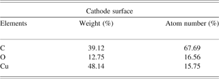
Surprisingly, after high-current pulsed-discharge, there is a significant deposition of anode material, Cu atom, on the fiber surface (see Fig. 7b and Table 3). This clearly indicates the material transfer from anode to cathode. For Cu, the mass per unit charge removed from anode is ~10−2 g/C (Mesyats, Reference Mesyats2000). At the total beam charges of 1.7 mC, the transferred mass per pulse is ~17 µg. Considering the Cu mole mass 63.5 g/mol, the number of Cu atoms per pulse is calculated to be ~1.6 × 10¹⁷, which is in good agreement with the aforementioned result. After a certain number of discharges, the cathode appears to be covered with molten anode material. It is possible that the microexplosive process will occur in the material transferred from the anode. Thus, the fragments on the tip of carbon fiber are the Cu or carbides of Cu. Additionally, this indicates the backstreaming flow of anode ions produced by electron irradiation. Under the participation of anode ions, the beam current is developed into a bipolar flow.
Table 3. Elemental surface compositions on carbon fiber by EDS analysis after high-current electron emission
3.4. Anode Plasma Jet
To understand the physics processes of the anode, it is necessary to obtain data on the power density of the electron flow, bombarding the anode, q a. The value of q a can readily be found from the current density at the anode j a and the voltage across the gap ϕac, q a = j aϕac. Here, it is assumed that the beam current density is equal to the current density at the anode, j a = j b. The time dependence of beam power density q a(t) as the voltage pulse proceeded is shown in Figure 8. One can see that the peak value of power density exceeded 5 × 10⁷ W/cm2. Further, this curve has a triangle-like shape with a maximum q am at t m ≈ 100 ns. The average rate of rise of the power for the rising portion of the q a(t) can be characterized by the quantity ![]() a1 ≈ q am/t m. The rising edge of power density is fitted linearly. Thus, the rising rate of power density q˙a1 is calculated to be ~5.17 × 10¹⁸ W/(m2 · s). Additionally, the falling rate of power density q˙a2 ~1.2 × 10¹⁸ W/(m2 · s) was obtained.
a1 ≈ q am/t m. The rising edge of power density is fitted linearly. Thus, the rising rate of power density q˙a1 is calculated to be ~5.17 × 10¹⁸ W/(m2 · s). Additionally, the falling rate of power density q˙a2 ~1.2 × 10¹⁸ W/(m2 · s) was obtained.

Fig. 8. (Color online) Diode voltage pulse and beam power density. The rising edge of beam power density is fitted linearly.
For high-current vacuum device, plasma formation on the cathode surface is accompanied by strong light emission within the diode. Once the cathode appears, the light emission distribution indicates the plasma development within the diode. Figure 9 presents the light emission image for the carbon fiber cathode captured by a framing camera at ϕac = 350 kV and d ac = 19 mm. Overall, light emission was not uniform over the whole cathode surface, and many individual bright spots appeared. The bright spots with different intensities distributed along or close to the cathode perimeter, which is mainly due to the edge effect. Clearly, not the whole cathode surface does participate in the electron emission process. It seems that electron emission occurred at the half of the cathode area. If electron emission is only limited to the edge region, the local current density of kA/cm2 level is possible, as is expected. Further, the diffuse plasma almost filled the diode gap. Most notably, the anode plasma appeared, mainly due to the irradiation of pulsed electron beam. Actually, the plasma formation from cathode or anode indicates the liberation of a large amount of material matter or adsorbed gases through the application of a strong electric field.

Fig. 9. Light emission from the diode gap for the carbon fiber cathode. The black region indicates the plasma within the gap.
The anode plasma could be generated by either melting and subsequent evaporation of the anode material or by an electron stimulated desorption of the contaminants on the anode surface. The rate of neutral atom desorption is dN/dt = j bk/e, where k is an electron desorption coefficient. The desorbed gas expands into the vacuum gap with a velocity v, forming a layer of thickness δ = vt with an average density of n = N/δ = jbk/ev. Therefore, the rate of ion generation is dN i/dt = (j bnσi/e)δ = (j b/e)2kσit, where σi is the ionization cross section. The bipolar flow forms at ![]() where m and M are the electron and ion mass, respectively. Thus, the time required for the formation of bipolar flow can be calculated as t biploar = e(m/M)1/2/j bkσi. At j b ≈ 200A/cm2 (the emission area being the half of the cathode area, see Fig. 9), k = 5 atoms/electron that is close to the upper limit of the total (cathode and anode) out-gassing (Shiffler et al., Reference Shiffler, Ruebush, Haworth, Umstattd, Lacour, Golby, Zagar and Knowles2002), σi = 3 × 10⁻¹⁸ cm2, and M/m = 2.9 × 10⁴ for oxygen atoms, t bipolar ≈ 300 ns can be obtained. Here the time required for the formation of bipolar flow is consistent with the prediction of P(t) (see Fig. 6). It should be pointed out that this is a crude estimation. Overall, the appearance of bipolar flow is closely related to the beam current density and pulse duration. Indeed, the bipolar flow does not appear at a low beam current density or t biploar larger than the pulse duration.
where m and M are the electron and ion mass, respectively. Thus, the time required for the formation of bipolar flow can be calculated as t biploar = e(m/M)1/2/j bkσi. At j b ≈ 200A/cm2 (the emission area being the half of the cathode area, see Fig. 9), k = 5 atoms/electron that is close to the upper limit of the total (cathode and anode) out-gassing (Shiffler et al., Reference Shiffler, Ruebush, Haworth, Umstattd, Lacour, Golby, Zagar and Knowles2002), σi = 3 × 10⁻¹⁸ cm2, and M/m = 2.9 × 10⁴ for oxygen atoms, t bipolar ≈ 300 ns can be obtained. Here the time required for the formation of bipolar flow is consistent with the prediction of P(t) (see Fig. 6). It should be pointed out that this is a crude estimation. Overall, the appearance of bipolar flow is closely related to the beam current density and pulse duration. Indeed, the bipolar flow does not appear at a low beam current density or t biploar larger than the pulse duration.
The anode plasma contained simultaneously charged ions and excited atoms of the anode material and of the adsorbed gas. From Figure 9, one can see that the anode plasma expands into the vacuum gap in the form of plasma jet. Thus, it is necessary to investigate the expansion velocity of anode plasma jet. It has been found that the purely thermal mechanism of destruction of the anode can be realized only if the specific energy input into the metal is not over (1–3)w s, where w s is the sublimation energy of the anode material. To estimate the expansion velocity of anode plasma jet, it is necessary to check the possible specific energy delivered to the anode surface within a characteristic time t m. Then the specific energy delivered to the anode will be determined as
where ρ and ![]() are, respectively, the anode material density and the average incident depth of beam electrons. Further, the average incident depth
are, respectively, the anode material density and the average incident depth of beam electrons. Further, the average incident depth ![]() should be estimated before the calculation of w a. The average incident depth
should be estimated before the calculation of w a. The average incident depth ![]() can be described as (Qin et al., Reference Qin, Wang, Dong, Hao, Liu, Zou, Wu and Guan2003)
can be described as (Qin et al., Reference Qin, Wang, Dong, Hao, Liu, Zou, Wu and Guan2003)
where eϕ is the average electron energy (in eV), ρ is the material density (in g/cm3), and ![]() is the incident depth (in cm). The thickness of layer 1 in the cross section of Cu target represents the incident depth of beam electrons (20–25 µm). Based on Eq. (3), only at ϕ = 100 kV, an average incident depth of beam electrons
is the incident depth (in cm). The thickness of layer 1 in the cross section of Cu target represents the incident depth of beam electrons (20–25 µm). Based on Eq. (3), only at ϕ = 100 kV, an average incident depth of beam electrons ![]() = 23.6 µm can be obtained. That is, the prediction of Eq. (3) is consistent with the observed result in Figure 4b, only at the average electron energy eϕ = 100 keV. Thus, at
= 23.6 µm can be obtained. That is, the prediction of Eq. (3) is consistent with the observed result in Figure 4b, only at the average electron energy eϕ = 100 keV. Thus, at ![]() = 23.6 µm and ρ = 8.9 g/cm3, the specific energy delivered to the anode by the irradiation of pulsed electron beam is calculated, as shown in Figure 10. One can see that in the rising stage of accelerating pulse, the maximum specific energy is ~105 J/g.
= 23.6 µm and ρ = 8.9 g/cm3, the specific energy delivered to the anode by the irradiation of pulsed electron beam is calculated, as shown in Figure 10. One can see that in the rising stage of accelerating pulse, the maximum specific energy is ~105 J/g.

Fig. 10. (Color online) Specific energy delivered to the anode by the irradiation of pulsed electron beam.
It has been shown that the interaction of the primary electron beam, the secondary ions, and the X-rays with the anode plasma material is slight (Qin et al., Reference Qin, Wang, Dong, Hao, Liu, Zou, Wu and Guan2003). It follows that the internal energy of the anode plasma material is determined by the parameters of the primary electron flow incident on the anode. Assuming that the anode plasma consists entirely of the anode material vapor and plasma, the expansion velocity of anode plasma jet can be determined. It has been shown that the velocity of motion of the forward layers of the plasma, V a, is described as (Mesyats, Reference Mesyats2000)
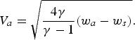
For w a = 105 J/g and w s = 5.34 × 10³ J/g, using γ = 5/3 for monatomic gases, the expansion velocity of anode plasma jet can be calculated to V a ≈ 3 cm/μs. Once the anode plasma appears and expands into the vacuum gap, the gap closure will be worsened further, with the combination of cathode-and-anode plasma expansions.
3.5. Thermal Regime of the Anode
The major energy of incident electrons is transformed into the thermal energy on anode surface, allowing a high target temperature. Thus, it is necessary to consider the thermal region of the anode. A one-dimensional heat equation for the x axis directed perpendicular to the anode surface can be described as
Here, c is the specific heat, λ is the heat conductivity, g(x, t) is the absorbed energy per unit volume by electron-beam irradiation. For simplicity, it is assumed that electrons lose their energy uniformly over the range ![]() . Thus, g(x, t) can be given as g(x, t) = q a(t)f(x) where the distribution function for the electron energy losses in depth f(x) takes the form
. Thus, g(x, t) can be given as g(x, t) = q a(t)f(x) where the distribution function for the electron energy losses in depth f(x) takes the form
Further, the power density can be expressed as
when the losses for evaporation are insignificant, the boundary conditions have the following form
In a short-period pulse, the heat release in the anode bulk can be neglected, the solution to Eq. (5) is
At t = t m, the surface temperature reaches up to T(t m) = 448.9 K. Next, the surface temperature still grows, although the beam power density starts to decrease. At t > t m, the surface temperature can be described as
where, w(t) = (q amt − q˙a2t 2/2)/(![]() ρc). Notably, the assumption, that the electron energy losses are uniformly distributed in depth, may result in a somewhat underestimated value of the anode temperature since the electrons lose some part of their energy near the surface.
ρc). Notably, the assumption, that the electron energy losses are uniformly distributed in depth, may result in a somewhat underestimated value of the anode temperature since the electrons lose some part of their energy near the surface.
Based on Eqs (9) and (10), the evolution process of anode surface temperature is presented in Figure 11a. At the end of the accelerating pulse, the anode temperature increases up to T m = 1420 K, significantly exceeding the melting point of Cu. By the time difference of anode surface temperature, the rising rate of anode surface temperature can be obtained, as shown in Figure 11b. One can see that the rising rate of anode surface temperature is calculated to be at a level of 109 K/s. Under such a heating rate, the energy loss due to the thermal conduction can be neglected, and the fast material melt can be achieved. Also, it provides a possibility to form a uniform material distribution in the melting layer. Further, the temperature gradient can be calculated approximately by (T(t) − T 0)/![]() . It was found that a large temperature gradient in the incident depth forms, on the order of 107 K/m. Thus, a nonequilibrium temperature field appears in the anode surface, simultaneously causing the formation of internal stress including elastic stress wave, quasistatic stress, and shock stress wave etc. The microscopic morphology of cross section of target may be attributed to the combining action of the temperature field and stress field by the irradiation of electron beams.
. It was found that a large temperature gradient in the incident depth forms, on the order of 107 K/m. Thus, a nonequilibrium temperature field appears in the anode surface, simultaneously causing the formation of internal stress including elastic stress wave, quasistatic stress, and shock stress wave etc. The microscopic morphology of cross section of target may be attributed to the combining action of the temperature field and stress field by the irradiation of electron beams.

Fig. 11. (Color online) Evolution process of anode surface temperature in electron-beam heating (a), its rising rate (b) and temperature grad (c).
After the heating of pulsed electron beams, the anode material cooling starts. In this process, the thermal conduction is dominant. Thus, the cooling rate can be estimated by solving the thermal conduction equation. The thermal conduction equation is described as following
where ![]() , c = 390 J/(kg.K) is the specific heat, λ = 380 W/(m.K) is the heat conductivity, and ρ = 8.9 × 10³ kg/m3 is the material density. The boundary condition is given as
, c = 390 J/(kg.K) is the specific heat, λ = 380 W/(m.K) is the heat conductivity, and ρ = 8.9 × 10³ kg/m3 is the material density. The boundary condition is given as
where r b is the microbeam radius. The solution to Eq. (11) can be expressed as
![T\lpar t\rpar = {1 \over {a \sqrt {\pi t} }}\bigg[ T_m \vint_0^{r_b } {\exp \left( \!\!-\! {{r^2} \over {4a^2 t}}\right) dr + T_0 \vint_{r_b }^\infty {\exp \left( \!\!-\! {{r^2 } \over {4a^2 t}}\right) dr} } \bigg] \eqno\lpar 13\rpar](https://static.cambridge.org/binary/version/id/urn:cambridge.org:id:binary:20151022040714489-0722:S0263034609990231_eqn13.gif?pub-status=live)
Figure 12a presents the cooling process of target material after the irradiation of electron beam, assuming r b = 100 µm. One can see that the cooling process lasts from T m to room temperature T 0, for several hundreds of microseconds. Additionally, the cooling rate is obtained by the time difference of Eq. (13), as shown in Figure 12b. The cooling rate is on the order of 107 K/s, and thus significantly lower than the heating rate. Moreover, the cooling rate exceeding 0.7 × 10⁷ K/s is focused on the time interval of ~50 µs, which is accompanied by a relatively slow process. Under such a cooling rate, it seems likely that the minicrystal layers form by the surface treatment of pulsed electron beams.

Fig. 12. (Color online) (a) Cooling process of target material after the irradiation of electron beam and (b) its cooling rate.
4. CONCLUSIONS
Based on a relativistic electron-beam accelerator with inductive energy accumulation, the layer structure, plasma jet, and thermal dynamics of Cu target under the irradiation of pulsed electron beam are investigated. Also, a description of a relativistic electron beam source with a carbon fiber cathode is given. Subjected to the irradiation of electron beam with a ~13 J/cm2 energy density, microcraters with 0.5–1 µm diameter appeared on the target surface, and the target cross section is characterized by multilayer structures with a ~20 µm thickness melting layer and a cellular layer. It was found that the carbon content increased significantly not only on the target surface but also on the cross section. Further, the diode operated under space-charge limited emission. The gas liberation per pulse induced by electron beam is analyzed. The total number of molecules desorbed from the anode reaches 1.1 × 10¹⁷. The planar diode perveance is revised, taking the edge emission and 2D effect into account. A good agreement between the experimental and calculated perveances was observed, assuming the gap closure velocity to 1.8 cm/μs due to the formation of cathode plasma. However, close to the end of the accelerating pulse, the experimental perveance exceeded the theoretical prediction, possibly indicating the participation of ion flow from the anode target. In the pulsed emission, there existed material transfer from anode to cathode, which was observed by the identification of elemental compositions on cathode surface. Furthermore, the transferred mass per pulse was estimated to be ~17 µg. The anode plasma is generated by either melting or subsequent evaporation of the anode material or by an electron stimulated desorption of the contaminants on the anode surface. As the beam energy was deposited on target surface, the anode plasma jet was observed by capturing the light emission within the diode gap, and expanded towards the cathode at a velocity of ~3 cm/μs. Here, the plasma jet is calculated by the specific energy delivered to the anode. Additionally, the time required for the formation of a bipolar flow is crudely estimated, and it is closely related to the beam current density and pulse duration. The estimated result is consistent with the prediction of diode perveance. By solving the one-dimensional heat equation, 109 K/s heating rate and 107 K/m temperature gradient can be obtained. It should be pointed out that the thermal conduction is not considered, which is reasonable under the condition of several hundreds of nanoseconds. After the heating of pulsed electron beam, the thermal conduction remains dominant, with a cooling rate on the order of 107 K/s. Overall, these results were made based on a relativistic electron beam source using carbon fiber cathodes. Therefore, the relativistic electron beam sources may provide a potential development for target experiments and high energy density physics.
ACKNOWLEDGMENT
This work was supported by the National High Technology Research and Development Program of China.