


1. INTRODUCTION
In recent years, extensive efforts have been made to develop compact high-power lasers for several applications as the ignition of laser fusion targets, the acceleration of electrons and ions, proton therapy, and laser ion sources with and without post-acceleration systems.
Simultaneously, new approaches are being investigated in several laboratories such as at the National Institute for Nuclear Physics (INFN) (Italy) by Torrisi et al. (Reference Torrisi, Cavallaro, Giuffrida, Gammino and Ando’2010) and at the IPPLM (Poland) by Wołowski et al. (Reference Wołowski, Badziak, Czarnecka, Parys, Pisarek, Rosinski, Turan and Yerci2008) to generate a large number of ions per laser shot, high-charge state, and energy of particle streams at low-cost and using flexible post-ion acceleration systems. The starting point is the production of ions from a solid target irradiated by a low-cost laser, with the goal being surface modifications produced by high-dose multi-energy ion implantation controlled by laser irradiation.
The energy of emitted ions can be enhanced using a post-acceleration system based on the use of a tailored ion-extraction chamber (EC). The ion extraction is realized by a high electric field of the order of 1–50 kV/1 cm, producing Coulomb repulsion and kinetic energy proportional to the ion charge state. The features of the multi-species and multi-energy of emitted ions, make the produced streams of particles suitable for implantation at different depths as well as for the modification of the structural, chemical, and physical properties of the implanted materials. The laser–plasma-generated ions can reach the substrates by direct ion implantation or by post-acceleration voltage. Currently, the properties of ions implanted in SiO2 films are being studied. Between the many infrared bulk transmitting substrate materials, germanium (Ge) is the most attractive due to its highest refractive index (n ~4.0), low dispersion properties at different temperatures, good thermal conductivity, non-toxicity, and non-hygroscopicity, as well as the possibility to change its conductive and optical properties by ion implantation processes. The attention of researchers worldwide is mainly focused on its application in the fabrication of optical devices, solar cells (Onyegam et al., Reference Onyegam, Sarkar, Hilali, Saha, Rao, Mathew, Jawarani, Mantey, Ainom, Garcia, James and Banerjee2013), waveguides (Kim et al., Reference Kim, Takenaka, Osad, Osada, Hata and Takagi2014), and sensors (Kaufmann et al., Reference Kaufmann, Isella, Sanchez-Amores, Neukom, Neels, Neumann, Brenzikofer, Dommann, Urban and von Kanel2011). In microelectronics, bulk Ge exhibits a great mobility of electrons and holes responsible for the speed and drive current of complementary metal–oxide–semiconductor-based logic devices (Chui & Saraswat, Reference Chui, Saraswat, Claeys and Simoen2007), but the properties of Ge ions implanted in SiO2 films have not been quite sufficiently investigated. In this paper, Ge ions have been implanted in SiO2 layers using medium-intensity lasers and two different approaches to evaluate the physical and chemical changes of Ge ions implanted in SiO2 layers as a consequence of the laser–plasma ion implantation parameters. Conventionally, the manufacturing of Ge layers into silicon (Si) occurs by using ion accelerators, which are time-consuming and costly. Through other methods, the implantation by laser has been developed over the past few decades, but there is still much to be done to improve the technology as well as to understand the mechanisms. The presented system opens a good opportunity for the development of compact and low-cost ion accelerators.
2. EXPERIMENTAL SETUP
At the INFN, Italy, a Nd:YAG laser system was focused on a 2-mm-thick Ge target mounted on a rotating carousel. The laser settings were the following: a laser energy of 500 mJ, a wavelength of 1064 nm; a pulse duration of 9 ns; the laser intensity of 1010 W/cm2, and a 10-Hz-repetition-rate mode. The pressure in the scattering chamber was 10−6 mbar. Figure 1 shows a sketch of the experimental setup employed to enhance the energy of the ions emitted by the laser–target interaction. The laser beam passed through an input hole located in a side of the parallelepiped EC with the longitudinal axes orthogonal to the target surface. The accelerating system consisted of 12 aluminum collimating discs [the last of which was the ground electrode (GE), located outside the EC] along the longitudinal axes and had a hole located 15 cm from the target. The parallelepiped EC was 26 cm long, 11 cm wide, and 11 cm high. Both the target and the EC walls were positively polarized at high voltage. The accelerating gap between each disc was 1.3 cm large and the irradiating area was 0.78 cm2. A resistive circuit consisting of resistors of 1 MΩ each was connected between the EC and the GE to maintain the accelerating voltage constant during the ion extraction. Inside the EC, the ions were accelerated only by the plasma and no potential bias was applied, whereas at the output of the EC, the post-acceleration system was employed using 30 kV accelerating voltage.
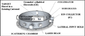
Fig. 1. The experimental setting from the INFN, Catania, Italy.
The emitted ions were accelerated by a bias voltage applied between the EC and the grounded cylindrical electrode. They went out of the EC through a hole 12 mm in diameter and at the end of a free flight, they reached the substrates. The acceleration voltage was maintained at the constant value of +30 kV during the laser irradiation in the repetition-rate mode. The maximum power supply current was maintained at 300 mA during the plasma injection as well. Simulations using the Opera three-dimensional (3D) code and taking into account the Boltzmann energy distribution (Torrisi, Reference Torrisi2016) of the ions emitted from the target and the iso-potential lines in the extraction area provided the evaluation of the ion trajectory from the target to the implanted substrates as described in detail in the previous paper (Torrisi et al., Reference Torrisi, Cavallaro, Giuffrida, Gammino and Ando’2010). Three Si substrates with a dioxide layer of 50 nm were placed at a distance of approximately 100 cm from the target, implanted after 10,000 and 50,000 laser shots (using the post-acceleration system ON) and deposited after 20,000 laser shots (using the post-acceleration system OFF) delivered against the Ge target. The fast-ion current providing signals proportional to the ion current as a function of time was measured by a Faraday Cup (ion collector, IC) placed at a distance of 100 cm from the irradiated target.
The data were collected using a fast storage oscilloscope (TekTronix TDS5104B, 2 GHz, 5 GS/s). Spectral reflectance measurements were conducted by means of an AvaSpec-2048 spectrophotometer with UB-600 lines/mm grating, a bandwidth of 195–757 nm and the angle of incidence at 15°. AvaLight-DH-S, consisting of a combined deuterium–halogen light source by Avantes for measurements in the range of 175–2500 nm, was employed. The AvaLight-D(H)-S features an integrated Through-The-Lens-shutter and filter holder for filters of up to 50 × 50 × 5.0 mm3. The holder was designed and built at the Nuclear Physics Institute of the Academy of Sciences of the Czech Republic. The home-made holder is made of gray anodized aluminum; it enables the positioning of the probe tip at different incidence and collection angles: 15°, 30°, 45°, and 75°. Both the used probes for illumination and detection were 1.5 mm in diameter. All eight holes are equipped with a setscrew to mount the probes or fibers into position. Figure 2 reports the experimental setup as follows: the light impinged on the substrate at an incidence angle of −15° with respect to the normal to the target plane and the optical spectrometer detected at +15°. The purpose is to evaluate the reflectivity for each investigated substrate.
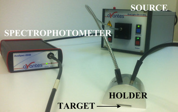
Fig. 2. An angled fiber probe holder for reflection measurements at different angles.
The structure, composition, and ion-depth distribution of thin layers onto the implanted substrates were investigated by Rutherford backscattering spectrometry (RBS) (Torrisi & Cutroneo, Reference Torrisi and Cutroneo2016). At the Tandetron laboratory of the Nuclear Physics Institute in Rez (Czech Republic), 2.0 MeV of He2+ ions were accelerated to impinge on a substrate at an incidence angle 0°, and the energy distribution and yield of backscattering He2+ ions at 170° below the entering beam were measured by a Si barrier surface Ortec Ultra detector and processed by SIMNRA software (Mayer, Reference Mayer, Duggan and Morgan1999). The alpha particle current density was about 4.5 nA/mm2 and the vacuum in the scattering chamber was 10−6 mbar. Since the backscattering cross-section for each element is known, it is possible to obtain a quantitative compositional depth profile from the RBS spectrum for films that are <1 µm thick.
The morphology of the implanted substrates was characterized by atomic force microscopy (AFM) analysis (Lavrentiev et al., Reference Lavrientev, Stupakov, Pokorny, Lavrentieva, Vacik, Dejneka, Barchuk and Čapková2015) using a NTEGRA AURA instrument (NT-MDT) in the tapping mode in the room atmosphere and at room temperature. A chip (NSG01) with the radius <10 nm was used. The root-mean-square roughness (RMS) as the standard deviation of the distribution of surface heights (Gadelmawla et al., Reference Gadelmawla, Koura, Maksoud, Elewam and Soliman2002) was estimated.
The wettability of the implanted samples was evaluated by a micropipette of 2 µl used to deposit a drop of distilled water at room temperature on the substrate. The contact angle was measured in the equilibrium state 20 s after the drop deposition (Kubiak et al., Reference Kubiak, Wilson, Mathia and Carras2011). Figure 6 shows the images of the contact angle measurements captured using a digital camera and Golden Ratio software. Each evaluation of the contact angle was obtained as an average of five measurements at different places on the substrates, with the error being ±2°.
3. RESULTS
3.1. Post-acceleration of ions by laser-generated plasma
The described experiment has been performed at a laser intensity of the order of 1010 W/cm2, the plasma temperature ranged between 10 and 50 eV, and the maximum plasma density, just at the end of the laser–matter interaction, was of the order of 1017/cm3. Both temperature and density decrease exponentially as the distance from the target increases. In the backward plasma acceleration regime, the ions emitted from the surface heated by the laser were directed toward the laser.
The high electron mobility as well as the low ion mobility produce the high electric field developed in front of the target, which is responsible for the ion's driving and acceleration along the normal to the target surface. This plasma acceleration is controlled by the non-equilibrium processes occurring in the plasma and can be modified by varying the laser intensity, the irradiation conditions, and the target composition.
In our experiment, energies with protons up to 100 eV and heavier ions up to about 100 eV/charge state have been obtained. The post-acceleration method is based on the use of a positive voltage applied to the target as well as to the EC, with the aim to enhance the energy of the extracted ions. In this way, the Coulomb repulsion makes it possible for ions to go through the little hole at the end of the free flight in the EC. Figure 3a, 3b provides a comparison between two spectra in time-of-flight (TOF) configuration for Ge ions produced by laser–plasma using (Fig. 3b) or without (Fig. 3a) 30 kV post-acceleration.
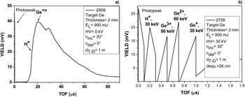
Fig. 3. The integral current signal of Ge ions collected by an IC with 0 kV (a) and 30 kV (b) of acceleration voltage.
The first peak in the figures, at 0 µs, marks the X-ray flash from the target due to the photoelectric effect indicating the starting point of the laser–matter interaction. The other arrows point out the larger peaks of the different ions emitted. The signal of protons (the faster ions) is detected at about 12 µs in the first spectrum (Fig. 3a) and 0.11 µs in the second one (Fig. 3b), corresponding to 36 and 30 keV, respectively. The peak of Ge ions is detected at 20 µs when no acceleration voltage is applied (Fig. 3a) and between 0.4 and 1.0 µs under an acceleration voltage of 30 kV of (Fig. 3b). The emitted Ge ions exhibit a corresponding average energy of 944 eV when the post-acceleration is switched off and of about 90, 60, and 30 keV when the post-acceleration is switched on, indicating that three main charge states are produced. In the second case, the energy is calculated using three different flight distances: the target-extraction hole of 15 cm distance, at which the plasma expands without post-acceleration, the 11 cm distance, at which the electric field of extraction is applied, and the 74 cm of free-flight distance. The first 26 cm of the distance are paths recorded by TOF spectra over a longer period of time.
The main TOF delay in the spectrum of Figure 3b is caused by an equivalent acceleration distance of about 26 cm. Three peaks are evident, corresponding to the Ge-ion acceleration at 90, 60, and 30 keV, resulting from the acceleration of the Ge+, Ge2+, and Ge3+ charge states, respectively. The 30 keV protons are detected at the TOF of about 0.11 µs. In the experimental conditions used, the extracted ion streams are thus practically composed of protons at 30 keV and of Ge ions at 30, 60, and 90 keV having comparable currents. The presence of only three charge states is caused by the mean electron energy of the plasma that does not make it possible to ionize the Ge ions up to Ge4+, being their fourth ionization potential of 45.7 eV, as reported in the NIST database 2016 (NIST, 2016). This means that the plasma temperature should be lower than 45 eV and higher than 34 eV, corresponding to the ionization potential of the Ge2+.
The number of protons produced per laser shot was calculated based on their yield being of about 20 mV at 0.15 µs. Since the input resistance of the fast storage oscilloscope is 50 Ω, the number of protons per laser shot is
 $$N_{\rm p} = \displaystyle{V \over R}\displaystyle{{{\rm \Delta} t} \over e} = \displaystyle{{20\,{\rm mV}} \over {50\,{\rm \Omega}}} \displaystyle{{0.15\,{\rm \mu s}} \over {1.6 \times {10}^{ - 19}\,{\rm C}}} = 3.8 \times 10^8{\rm protons/laser shot}. $$
The measurements have been performed using an IC with a 4 mm2 surface area to collect focalized ions coming from the post-acceleration system. It means that the number of detected protons is about 1010 protons/cm2 per laser shot. Using 104 laser shots, the proton implantation dose is thus of about 1014/cm2. When the Ge ion yields of Ge+, Ge2+, and Ge3+ are taken into account, similar considerations indicate that the total number of Ge ions produced using 104 laser shots is of the order of 2 × 10¹⁴/cm2.
3.2. RBS measurements
Ge ions at energies of 30, 60, and 90 keV were implanted into 50-nm-thick SiO2 films grown on Si wafers by oxidation in a dry-oxygen ambient at a temperature of 1000 °C. In order to evaluate the deposition and implantation of Ge atoms as well as their position in the SiO2 layer covering a Si substrate, the RBS surface analysis is applied. The Stopping and Range of Ions on Matter (SRIM) code (Ziegler, Reference Ziegler2010) makes it possible to calculate in SiO2 the range of Ge-implanted ions of 26, 46, and 63 nm for 30, 60, and 90 keV, respectively.
Figure 4a reports a typical RBS spectrum relative to Ge-atom deposition on the SiO2-substrate surface. It has been obtained using the atoms and neutral species produced by the laser-generated plasma and deposited, without post-acceleration, on the substrate surface. Figure 4b reports a typical SRIM simulation of the 90 keV Ge ions implanted in the SiO2 substrate performed with 104 ions. Figures 4c and 4d report the RBS spectra relative to the Ge ion depth penetration up to 30 nm (Fig. 4c) and 51 nm (Fig. 4d), respectively.

Fig. 4. The RBS spectra of SiO2/Si substrates deposited by Ge atoms (20,000 laser shots) (a), a SRIM simulation of 90keV implanted ions (b), and Ge implantation after 10,000 shots (c), and 50,000 shots (d), respectively.
The RBS spectra are relative to the deposition of Ge ions produced after 2 × 10⁴ laser shots (Fig. 4a), and implantations after 1 × 10⁴ laser shots (Fig. 4c) and 5 × 10⁴ laser shots (Fig. 4d). Moreover, RBS analyses are performed on a randomly oriented substrate (random spectrum) and under the conditions of ion channeling (aligned spectrum). The energy of emitted Ge ions is sufficient to produce a slight damage to the crystalline structure of the substrate due to the high nuclear stopping power of the low-energy Ge ions. A comparison between the reported spectra shows that the peak of the implanted species does not decrease in yield, demonstrating that the interstitial defect and surface amorphization occur as a result of Ge-ion implantation. The little scattering at shallow depths in a near-perfect crystal is exhibited due to the low thickness of the germanium film deposited on the substrate surface. The maximum atomic concentration of Ge ions in the deposited layer was 100% at 300 nm; in the implanted ones, the maximum concentrations were 5.8% at 29.6 nm (Fig. 4b) and 10% at 51 nm (Fig. 4c).
The energy loss and range of the post-accelerated Ge ions implanted in Si can be theoretically calculated by the SRIM code. The simulation provides a range of 28, 47, and 66 nm for 30, 60, and 90 keV Ge ions in Si, respectively. The energy loss of ions due to the electronic stopping power is 54, 77, and 95 keV/μm, while that due to the nuclear stopping power is 924, 1,069, and 1,133 keV/μm, respectively, demonstrating that the high nuclear stopping power may produce damage to the Si structure at high implanted doses. These results are in good agreement with the experimental results obtained by the RBS analysis and specifically with preliminary RBS ion channeling analysis, showing the damage to the crystal surface of the semiconductor.
3.3. Optical measurements
The aim of this study is to characterize optically the surface of ion-implanted surfaces. For this purpose, the surface reflection spectra were recorded at room temperature by using a spectrometer in the wavelength range of 300–800 nm. Figure 5a reports the reflectivity–measurement curves for all the investigated samples against the wavelength, going through seven main peaks at 370.7, 465.7, 486.4, 581, 610.3, 674.8, and 691 nm. The measurements are relative to the following sample surfaces:
-
#1: Ge deposited in SiO2/Si using 2 × 10⁴ laser shots;
-
#2: virgin Si;
-
#3: Ge implanted in SiO2/Si with 5 × 10⁴ laser shots;
-
#4: Ge implanted in SiO2/Si with 1 × 10⁴ laser shots;
-
#5: virgin SiO2/Si.
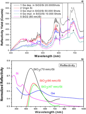
Fig. 5. Experimental optical reflectivity measurements (a) and the data from the literature (b) for all the samples investigated.
The reflectivity trend for the investigated samples was expected, because metallic particles are efficient to enhance the optical effects (Pham et al., Reference Pham, Matz and Seifarth1997), and confirmed by the Ge-film surface deposition. In the wavelength range from approximately 300 to 400 nm, the reflectivity of both #2 and #5 was prominent as well overlapped in 700–750 nm wavelength range, whereas between 400 and 755 nm, is dominant for sample #1. Between 600 and 755 nm, samples #3 and #4 were comparable and occasionally overlapped. A preliminary comparison between SiO2/Si with a dioxide layer of 60 and 200 nm has corroborated that a decrease in the thickness of the dioxide layer actually decreases the reflectivity; the thin-film thickness depends linearly on the wavelength at which the minimum spectral reflectance occurs (Hlubina et al., Reference Hlubina, Lunacek and Ciprian2009). The measurements are in agreement with the literature data reported in the rebuilt plot of Figure 5b using by (Honsberg & Bowden, Reference Honsberg and Bowden2016; Janos Technology IR, 2016; Leem et al., Reference Leem, Lee, Jun, Heo, Park, Park and Yu2014.
3.4. Wettability
Wettability is the tendency of one fluid to adhere to a solid surface. Wettability analysis is one of the many surface analyses demonstrating a change of properties due to ion-implantation effects. A liquid drop poured onto a solid surface forms a ‘cap’ and formed three-phase line at the equilibrium corresponds to the minimum energy state. The contact angle is identified at the meeting point between the solid–liquid and solid–vapor interfaces (Cutroneo et al., Reference Cutroneo, Torrisi, Ullschmied and Dudzak2016).
The Young equation describes the balance at the three-phase (i.e. solid, liquid, and vapor) contact:
 $${\rm \gamma}_{{\rm SV}} - {\rm \gamma}_{{\rm SL}} = {\rm \gamma}_{{\rm LV}}\,{\rm cos}\,{\rm \theta}, $$
where γLV is the surface tension at the interface of the liquid and the vapor phases, γSL at the interface of the solid and the liquid phases, and γSV at the interface of the solid and the vapor phases.
Conventionally, a surface where a liquid does not spread is indicated as θ≠0°; and when the liquid spreads freely over the surface at a rate depending on the liquid viscosity and solid surface roughness, the surface is indicated as θ = 0°. The tendency for the liquid to spread increases as θ decreases, so that the contact angle is a useful inverse measure of wettability. Figure 6 presents the experimental measurements of the contact angle of different liquids on pristine Si (Fig. 6d) and on a SiO2 layer on Si (Fig. 6e), as well as on Si substrates with Ge ions deposited after 20,000 shots (Fig. 6a), implanted after 50,000 shots (Fig. 6b), and implanted after 10,000 shots (Fig. 6c). The Si –water contact angle was approximately 37.9°, which is in the range measured by Osborne (Reference Osborne2009).

Fig. 6. Contact angle measurements on Si substrates with Ge ions: deposited after 20,000 shots (a), implanted after 50,000 shots (b) and after 10,000 shots (c), virgin Si (d), and a SiO2 layer on Si (e).
The less hydrophilic surface is thus represented by that of Ge deposited after 20,000 laser shots (Fig. 6a), while the most hydrophilic surface is represented by the virgin monocrystalline Si surface (Fig. 6d).
3.5. AFM measurements
Figure 7a shows the typical AFM images for a comparison of the SiO2/Si before the treatment (Fig. 7e) and after the ion deposition (Fig. 7a) and the ion implantation using 50,000 laser shots (Fig. 7b), 10,000 laser shots (Fig. 7c), and virgin Si (Fig. 7d). The monocrystalline Si substrate exhibits a roughness of 0.200 nm, whereas the SiO2 has the roughness of 0.251 nm. AFM analyses simply indicate the topography of the surface, but a strong difference is evident in the surface roughness on the deposited SiO2/Si substrate of 3.160 nm. This behavior is caused by the low dose as well as the low energy of deposited ions. The surface morphology depends on the ion dose. The surface is rough at a low dose (Fig. 7c), but becomes smooth (Fig. 7b) at a higher dose (Keiji et al., Reference Keiji, Shunichi, Wada, Suehara and Aizawa1996) due to the viscous relaxation induced by ions, neutrals and electrons (Oyoshi et al., Reference Oyoshi, Tagami and Tanaka1991). An increase in ion energy leads to a decrease in the particle size and a reduction in the surface roughness (Pham et al., Reference Pham, Matz and Seifarth1997) confirmed by Figures 7a and 7b. The substrate implanted after 10,000 shots exhibits an average roughness of 1.634 nm, with the maximum size being lower than 15 nm, whereas the substrate implanted after 50,000E shots exhibits a slight roughness of 0.264 nm and the size of the order of 1 nm. AFM images show that the SiO2/Si substrate deposited using 20,000 shots consists of particles with the maximum dimension lower than 30 nm and the same shape. In this case, the covering is quite uniform due to the contribution at low ion energy, producing a Ge deposition in the first surface layers of the substrate.
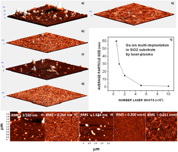
Fig. 7. 2D and 3D AFM images sized 2 × 2 µm2 related to Si substrates with Ge ions deposited after 20,000 shots (a), implanted after 50,000 shots (b), and after 10,000 shots (c); 2D AFM images sized 2 × 2 mm2 related to the virgin Si substrate (d), and the virgin SiO2 layer on Si (e); the plot of the average particles size as a function of the number of laser shots (f).
4. DISCUSSION AND CONCLUSIONS
This study demonstrates that the multi-ion implantation produced by the post-ion acceleration of laser-generated plasma is effective, useful, and promising. The results of the investigated surface treatment show that the post-acceleration system can be more efficient and cheaper than the conventional methods using ion implanters. The novelty of the present work with respect to that done by other researchers lies in improvements of the extractor system, making it possible to operate at a laser repetition rate of 10–30 Hz. Moreover, the electrical discharges in the vacuum chamber have been reduced by using a resistor withstanding higher voltage, covered with an insulating varnish, and also boron nitride separators between the discs of the post-acceleration system to prevent electrical discharges and conduction resulting from the deposition of a conductive carbon film formed during the prolonged process of plasma production. The new acceleration system may produce a continuous current of ions for a long period of time without a discharge. This paper focuses on both the post-accelerator laser system for the preparation of multi-energy ion beams and the study of the surface treatment depending on the ions deposited or implanted, represent the goal of this paper.
The observed changes in the multi-ion implanted substrates depend on the type of treatment and on the concentration of implanted or deposited ions.
Figure 4 illustrates the trend of the deposited and implanted ions by increasing the dose of Ge ions. Figure 5 shows that an increase in the number of laser shots increases reflectivity in implanted substrates. Moreover, a comparison between deposited and implanted Ge ions reveals higher reflectivity in the deposited substrate. The reason is that the deposition process induces defects and the development of amorphous Ge phases. A better evaluation of the Ge crystalline fraction is being worked on. Figure 6 shows a comparison between virgin, deposited, and implanted substrates for wetting-ability measurements. The contact angle increases, going from virgin SiO2 of 56.63° to the value of 76.47° for SiO2, with deposited and implanted Ge ions. If the surface is chemically hydrophilic, it will become less hydrophilic when it is implanted. This means that its surface roughness will be reduced by the ion implantation process, which produces ion sputter polishing.
The surface morphology strongly depends on the ion dose and on the energy of implanted ions. Rough surfaces or small particles of metals are more efficient in the amplification of the optical effect than smooth surfaces and macroscopic aggregates as revealed by a comparison between AFM, wettability, and optical measurements. In conclusion, this paper provides a comparison between laser-implantation with and without a device for the post-acceleration of ions laser–plasma-generated at 30 keV/charge state to implant Ge ions into Si substrates. For a wider diameter of the extraction hole of the grounded cylindrical electrode, the increase in the yield gradient of emitted ions was estimated from OPERA 3D simulations in the previous work (Torrisi et al., Reference Torrisi, Cavallaro, Giuffrida, Gammino and Ando’2010) by considering the same geometry and the same laser parameters but different irradiated targets from those used in the present work.
The presented concept of a versatile, compact, and cheaper accelerating module is based on the use of a medium-intensity laser to produce plasma pulses. The plasma expansion in a vacuum chamber enables ion emission and acceleration along the normal to the target surface at a low energy of the order of 100 eV per charge state. A further and significant ion acceleration can be achieved with an external and axial post-acceleration voltage, which increases the acceleration up to 30 keV per charge state. The extracted multi-energy ion beam, obtained using a repetitive laser pulse, makes it possible to implant the ions into different surfaces such as Si with a dose depending on the ion current and on the implanted time, significantly modifying the chemical and physical properties of the exposed surfaces.
This system has exhibited its potentiality beyond what conventional accelerator technologies can do. As reported, there is a significant scope for further effective development of this low-cost high-current ion post-acceleration system using, for example, stronger power supply able to support high electron and ion currents. This development will open new opportunities for the implementation of a current drive for table-top systems in advanced accelerator technology.
The increase of the ion acceleration voltage to 100 keV/charge state as well as the ion current up to 1015 particles/laser pulse is being worked on. Moreover, other surface characterizations of the roughness, hardness, wear, and chemical passivation are being prepared in order to prove the potentiality of the multi-implanted Si surface using Ge ions.
Acknowledgments
The research has been implemented at the CANAM (Center of Accelerators and Nuclear Analytical Methods) infrastructure LM 2011019 and was supported by project no. P108/12/G108.


