1. INTRODUCTION
Investigations into the impedance behavior of a diode during the generation of high-current density pulsed electron beams have been carried out since the 1970s. It has been shown that the electron current is limited either by the emission ability of the cathode or by the space charge in the anode–cathode (A–C) gap (Bugaev et al., Reference Bugaev, Krenydel and Shanin1984; Mesyats & Proskurovsky, Reference Mesyats and Proskurovsky1989). With high electron current density the collective space charge effects in the A–C gap become sufficient and, thus, the current density becomes limited by space charge of the electrons. If there is no deviation in electron trajectory from, then the current density is described by the one-dimensional Child–Langmuir relation (1D CL) (Langmuir, Reference Langmuir1913). The space-charge-limited current density for electrons, taking into account the reduction in the geometric gap spacing due to plasma expansion, is:
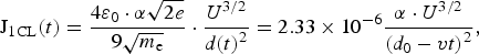 $${{\rm J}_{{\rm 1CL}}}(t) = \displaystyle{{4{{\rm \varepsilon} _0} \cdot {\rm \alpha} \sqrt {2e}} \over {9\sqrt {{m_{\rm e}}}}} \cdot \displaystyle{{{U^{3/2}}} \over {d{{(t)}^2}}} = 2.33 \times {10^{ - 6}}\displaystyle{{{\rm \alpha} \cdot {U^{3/2}}} \over {{{({d_0} - vt)}^2}}},$$
where U is the accelerating voltage, d 0 the initial A–C gap spacing, ε0 the absolute permittivity, m e the electron mass, e the electron charge, v the plasma expansion speed, and α the amplification coefficient, equal to 1.86 for a diode with bipolar flow of ions and electrons.
The collective effects in the A–C gap of a high-current electron beam diode also lead to a deviation of the electrons trajectory. At high electron current density the electron beam is compressed (or pinched) by its own magnetic field (Gao et al., Reference Gao, Qiu, Zhang, Zhang, Wang and Yang2010). With low electron current density, the beam spillage occurs due to Coulomb repulsion. In (Parker et al., Reference Parker, Anderson and Duncan1974) it is shown that electrons in a vacuum diode without an external guiding magnetic field are deflected by an angle of 40° (half-angle).
Our previous study (Pushkarev et al., Reference Pushkarev, Novoselov and Sazonov2007) shows the results of the current and charge balance in an electron diode of the TEU-500 electron accelerator (350–500 keV, 60 ns, 250 J/pulse). It is found that the electron deflection angle from the normal to the cathode surface is > 60°. At the moment, a great number of studies have been performed on the perveance of a planar diode during the generation of high-current electron beams in the absence of a longitudinal magnetic field in the diode gap. A detailed analysis of these studies can be found in (Pushkarev et al., Reference Pushkarev, Isakova, Sazonov and Kholodnaya2013). It was shown that the diode current is satisfactory described by Eq. (1) for the working surface of the diode, provided that current and voltage waveforms are measured correctly and parasitic pre-pulses are not present. Various effects, such as enhancement in the electron current due to reduction in the A–C gap spacing and increase in the cathode emission surface, as well as the presence of micro-protrusions on the cathode and counter ion flow are all well described by the 1D CL, if they are taken into account.
A study of a great interest is the analysis of the influence of curvature of the electrons trajectory in the A–C gap on the impedance of an ion diode with magnetic insulation. Space charge of ions limits the ion current density to 2–3% of the electron current density. Thus, to increase the efficiency of ion beam generation one needs to reduce the electron component of the total current in the diode. One method to suppress the electron flow in an ion diode is to use a transverse magnetic field (E⊥В). Under the influence of Lorentz force the electrons change their trajectory from moving across the A–C gap (from cathode to anode) to along the gap, moving along the cathode. The deviation angle is 90° (Humphries, Reference Humphries1990). Therefore, the possibility of describing the current–voltage characteristics of an ion diode with magnetic insulation using 1D CL is not obvious and requires experimental studies. The results of simulation of the ion and electron currents density in a planar ion diode with magnetic insulation are presented in (Bergeron, Reference Bergeron1976). The simulation showed that at an accelerating voltage of 50–500 kV and the magnetic induction below critical B cr the electron current density is 1.6–2 times higher than that predicted by Eq. (1) for unipolar flow in a diode. With an increase the in magnetic induction the electron current density is reduced to the values predicted by Eq. (1). The drift of magnetized electrons does not provide sufficient suppression of the electron current. Simulation of the reduction in electron current in a pinch-diode caused by an additional increase in the concentration of electrons in the A–C gap due to beam pinching is presented in (Ottinger et al., Reference Ottinger, Cooperstein and Schumer2001). It was found that deviation in the electron trajectory due to influence of self-magnetic field slightly reduces the current density, the suppression factor is ~1.4.
An ion diode operating in double-pulse mode is useful for studying the applicability of 1D CL ratio for calculation of the electron current in the diode. During the first voltage pulse the diode operates in the mode of electron beam generation with a weak influence of magnetic field. During the second pulse the electron current is significantly decreased compared with the 1D CL ratio. The purpose of the study is to analyze the applicability of 1D CL ratio for the calculation of the electron current in the A–C gap of an ion diode with self-magnetic insulation, operated in double-pulse mode.
2. EXPERIMENTAL SETUP
The experiments have been done using a planar strip diode with self-magnetic insulation of electrons on the TEMP-4M accelerator (Pushkarev & Isakova, Reference Pushkarev and Isakova2013; Pushkarev et al., Reference Pushkarev, Isakova, Sazonov and Kholodnaya2013). Figure 1 shows a photograph of the planar strip diode and waveforms of the accelerating voltage and total diode current.

Fig. 1. Photograph of the planar strip diode, waveforms of the accelerating voltage, total diode current, and calculated current for electrons. A–C gap spacing is 8 mm.
The anode is made from graphite, and the cathode from stainless steel. The cathode has 77 slits, 4 mm wide and 5 cm long, resulting in a transparency of 70%. The A–C gap spacing was chosen to match the diode impedance with that of the Blumline generator (4.9 Ω). In the optimized arrangement, the gap increases from 8 mm at the bolted end of the grounded electrode to 10 mm at the open end.
In a self-magnetically insulated diode, a transverse magnetic field is formed in the A–C gap by the self-diode current flowing through the cathode, which is grounded at one end only. The electrons will drift in the crossed E⊥B field, provided that the magnetic induction is sufficient to confine electrons along the cathode. The electrons, confined by a magnetic field, drift along the surface of the cathode from the bolted end (grounding point) toward the free end of the diode. A simplified mechanism illustrating electrons drift in ion diode is shown in Figure 2.
Fig. 2. Illustration of magnetized electron drift in a self-magnetically insulated ion diode.
The movement of electrons in the crossed electric and magnetic fields can be represented in the form of rotation at the cyclotron orbit and drift of the center of the circle in the direction perpendicular to the vectors E and B (movement of trochoid).
3. DIODE IMPEDANCE DURING THE FIRST VOLTAGE PULSE
A mandatory condition for suppression of the electron current in ion diodes with magnetic insulation is formation of the magnetic field in the A–C gap with the induction exceeding a critical value. The critical magnetic field can be calculated taking the condition when the height of the trochoid of drifting electrons in equal to the geometric A–C gap spacing (Fig. 2). Taking into account the reduction in A–C gap spacing due to plasma expansion, the critical magnetic induction is (Bystritskii & Didenko, Reference Bystritskii and Didenko1989; Morozov, Reference Morozov2006):
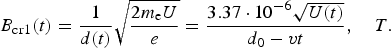 $${B_{{\rm cr}1}}(t) = \displaystyle{1 \over {d(t)}}\sqrt {\displaystyle{{2{m_{\rm e}}U} \over e}} = \displaystyle{{3.37 \cdot {{10}^{ - 6}}\sqrt {U(t)}} \over {{d_0} - vt}},\quad T.$$
Figure 3 shows calculation of the critical magnetic induction in the A–C gap of the planar strip diode during the first voltage pulse. During the first voltage pulse, the potential graphite electrode acts as a cathode and the stainless steel grounded electrode as an anode.
Fig. 3. Waveform of the accelerating voltage at the first pulse, the critical magnetic induction, and magnetic induction in the A–C gap.
In the studied diode, it is difficult to measure the magnetic induction, since the magnetic field is generated by the self-diode current only when a voltage of over 100 kV is applied. Thus, we performed simulation of the magnetic field distribution using the ELCUT field-modeling program, taking into account damping of the magnetic field due the cathode material. The simulation showed that the distribution of the magnetic field in the diode gap is uniform over the cross-section of the diode and magnetic induction is proportional to the total diode current. During the first voltage pulse the magnetic field is close to the critical value (see Fig. 3) and the electrons are deflected from the normal to the cathode surface at an angle of about 90° (Pushkarev et al., Reference Pushkarev, Isakova and Guselnikov2011).
Figure 4 shows the results of simulation of the motion of electrons in the A–C gap using the CST PARTICLE STUDIO (CST PS) simulation program.
Fig. 4. Trajectory of electrons in A–C gap at U = 250 kV; I = 10 kA (a) and 20 kA (b).
Below is a cathode, from which the emission of electrons occurs, while at the top is a current-carrying conductor (anode). The gap spacing between the electrodes is 8 mm. As can be seen from Figure 4, the current of 10–15 kA causes a significant deviation of electron trajectory from the normal to the cathode surface, but it is not sufficient for complete magnetic insulation.
Figure 5 shows the waveform of the accelerating voltage and experimental and calculated values of the diode impedance; gap spacing of 8 mm.
Fig. 5. Waveform of the accelerating voltage and impedance of the planar strip diode.
The diode impedance was calculated as:
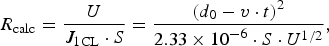 $${R_{{\rm calc}}} = \displaystyle{U \over {{J_{{\rm 1CL}}} \cdot S}} = \displaystyle{{{{({d_0} - v \cdot t)}^2}} \over {2.33 \times {{10}^{ - 6}} \cdot S \cdot {U^{1/2}}}},$$
where S is the cathode area.
During the first voltage pulse one can distinguish two modes of the diode operation: the mode of discrete emission surface and the mode of space-charge limitation. Since the application of the voltage and until the graphite cathode surface is covered by explosive-emission plasma (discrete emission surface mode, 0 < t < 250 ns in Fig. 5), the diode current is limited by the emission ability of the cathode. Moreover, in this time interval, when В > В cr (see Fig. 3) the electron current can be decreased by self-magnetic insulation. The diode impedance, in this case, is greater than the calculated values obtained under the condition of unlimited emission ability of the cathode. Decrease in the diode impedance is attributed to both: increases in the emission surface area on the graphite cathode and reduction in the A–C gap spacing due plasma expansion toward the anode [see Eq. (3)].
When the surface of the graphite cathode is covered by plasma (250 < t < 600 ns in Fig. 5), the total diode current is limited only by the electron space charge in the A–C gap. Experimental values of the diode impedance are well described by Eq. (3), with the plasma expansion speed of 1.2 ± 0.2 cm/μs and α = 1. The electron current on the first pulse is well described by 1D CL, although the trajectory of electrons is significantly deviated from the normal to the cathode surface (see Fig. 4), B ≈ B cr. These results coincide with the data obtained for high-current electron diodes (Pushkarev et al., Reference Pushkarev, Isakova, Sazonov and Kholodnaya2013), which confirms the correctness of measurement of current–voltage characteristics of the ion diode and the calculations. In an ion diode operating in space-charge mode, with magnetic insulation, the total ion current component is negligible due to low efficiency of ion beam generation, typically not exceeding 10–15%.
When analyzing the impedance diode, we did not take into account the influence of anode plasma. In fact, the electrons, which are accelerated in the diode gap, bombard the anode and thus cause the gas desorption. As a result of ionization of desorbed gas the plasma is formed, which expands toward the graphite cathode. It can cause an additional reduction in the A–C gap spacing. Furthermore, the anode plasma acts as a source positively charged ions. The appearance of the ion flow in the diode increases the electron current due to partial neutralization of the electron space charge. In such conditions, the electron current can exceed the 1D CL value (α = 1.86). The time of anode plasma formation can be estimated from (Li et al., Reference Li, Liu, Wan, Zhang, Wen and Liu2009):
 $${t_0} = \displaystyle{e \over {{\rm \gamma} \cdot {\rm \sigma} \cdot j}}\sqrt {\displaystyle{{{m_{\rm e}}} \over {{m_{\rm i}}}}},$$
where m i is the ion mass, σ the ionization cross-section, γ the desorption efficiency, and j the current density.
The 100–200 keV electron beam exposure to the anode surface yields to desorption of gas molecules with an efficiency of ten molecules on an electron (Abdullin & Bazhenov, Reference Abdullin and Bazhenov1984). At the current of 5–10 kA (see Fig. 1), and the cathode area of 100 cm2 the current density will be 50–100 A/cm2. The cross-section of ionization of nitrogen molecules is 3 × 10⁻¹⁸ cm2 (Abdullin & Bazhenov, Reference Abdullin and Bazhenov1984), the weight ratio of N+ ion and electron is equal to 2.5 × 10⁴. Then the duration for the formation of the anode plasma should be greater than 400 ns. Therefore, in our experimental conditions, the influence of the anode plasma to the diode impedance on the first pulse is insignificant.
4. SUPPRESSION OF ELECTRON CURRENT
The total diode current on the first pulse is well described by 1D CL, although the trajectory of electrons is significantly deviated from the normal to the cathode surface, B ≈ B cr. Our studied and analysis of the literature showed that ion diodes with self-magnetic insulation feature the reduction in the electron component of total current by a factor of 2–2.5 compared with 1D CL (Langmuir, Reference Langmuir1913; Pushkarev et al., Reference Pushkarev, Isakova, Sazonov and Kholodnaya2013).
4.1. Suppression of electron current during the second pulse
Figure 1 shows the waveforms, which characterize the operation of the planar ion diode in double-pulse mode, and calculated values of the electron current. Calculation of electron current in the diode during the first pulse was performed using 1D CL ratio, taking in the account the reduction in A–C gap spacing due to plasma expansion and α = 1. In calculation of the electron current in the diode during the second pulse we took into account the effect of plasma erosion (when accelerating voltage reverses polarity) (Pushkarev et al., Reference Pushkarev, Isakova and Guselnikov2011) and partial compensation of electron space charge by counter ion flow (α = 1.86):
 $${I_{{\rm e2}}}(t) = \displaystyle{{2.33 \times {{10}^{ - 6}} \cdot 1.86 \cdot {U^{3/2}} \cdot S} \over {{{[{d_0} - v(t - {t_0})]}^2}}},$$
where t 0 is the duration of the first voltage pulse (t 0 = 520 ns in Fig. 1).
Our studied showed that the total diode current is 2–2.5 times lower than calculated by 1D CL ratio. Figure 6 shows the calculation of the magnetic field in the A–C diode gap during the second pulse (calculation was performed using the ELCUT program for data in Fig. 1) and the change in the critical magnetic induction.
Fig. 6. Waveform of the accelerating voltage on the second pulse, the critical magnetic induction, and magnetic induction in the A–C gap.
The calculation of critical magnetic induction on the second pulse was made taking into account the reduction in A–C gap (due to plasma expansion) and the effect of plasma erosion. During generation of an ion beam, the magnetic induction in the A–C gap exceeds the critical value, which causes electrons, confined by magnetic field, drift along the diode. The length of the drift region is 200–220 mm with the A–C gap being 8 mm.
4.2. Single pulse operating mode of the ion diode
The ratio of electron current suppression was also estimated during the operation of the ion diode with self-magnetic insulation in single pulse mode. The generator, in this case, formed one voltage pulse of positive polarity; the potential electrode of the diode was the anode, and the grounded electrode was the cathode. In this mode, the anode plasma is absent and does not affect the total current in the diode, the latter is determined solely by the electron current from the cathode (no bipolar flow, α = 1). The absence of plasma on the anode surface is shown by the absence of ion current [according to measurements of ion current density by a Faraday cup and thermal imaging diagnostics (Isakova & Pushkarev, Reference Isakova and Pushkarev2013)]. The studies showed that experimental values of the total current are 2–2.2 times lower than that estimated by 1D CL ratio [Eq. (1)] at α = 1 (see Fig. 7).
Fig. 7. Waveform of the accelerating voltage, the ratio between calculated electron, and the total diode current in planar diode at different A–C gaps spacing.
In order to assess correctness of the electron current calculation by 1D CL ratio we performed studies of the diode in single pulse mode when the cathode was grounded at several points (conditions of insufficient magnetic insulation). In this case, the current through the cathode flows in several directions toward the grounding points. The current flowing in a particular area of the cathode is not sufficient to create a critical magnetic field and, thus, the movement of electrons in the A–C gap can be treated as 1D. Figure 8 summarizes various results of the ratio of total diode current (pulse amplitude) to the 1D CL calculated electron current.
Fig. 8. The dependence of the calculated electron current on experimental current measured when the cathode was grounded at several points.
It was found that in the conditions when magnetic insulation was violated the experimental values of the current at the maximum (where LdI/dt = 0) are in good agreement with the calculation [Eq. (1)]. This confirms the correctness of the use of 1D CL ratio for calculation of the electron current in the ion diode and the electron current suppression.
5 DISCUSSION OF THE RESULTS
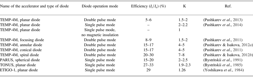
The results of studies on electron current suppression for different diodes with self-magnetic insulation are summarized in Table 1 (Pushkarev et al., Reference Pushkarev, Isakova and Khailov2015).
Table 1. Electron current suppression factor K for various diodes with self-magnetic insulation.
In an ion diode with self-magnetic insulation the increase in the electron drift path in crossed electric and magnetic fields is a necessary but not a sufficient condition for suppressing the electron current compared to the CL limit. If the accelerating voltage during electron drift changes insignificantly and the drift time is less than the transit time of ions in the A–C gap, then the total electron current in the diode will be well described by the 1D CL ratio, taking into account the working area of the cathode surface and partial compensation of electron space charge by counter flow of ions. In this case, there are no additional physical processes, which limit the electron current in an ion diode, except for the distortion of the electric field in the A–C gap by space charge of electrons. When an electron, under the influence of a magnetic field, is deviated from the normal to the cathode surface, its energy does not change, since the Lorentz force, which causes deviation is always directed perpendicular to the electron velocity vector. The linear electron velocity does not change, and the duration of acceleration at B < B cr may increase by no more than π/2 times. In this case, the acceleration time of C+ ions at an accelerating voltage of 200–300 kV will 100–120 times exceed the acceleration time of electrons. Since the electron energy does not change, when its trajectory deviates at B < B cr, that means that there is no change in the total diode current for a given accelerating voltage, therefore, the total current in the diode will be described by the 1D CL ratio, taking into account the area of the cathode. When the electrons drift in electric and magnetic field (at B>B cr) there is an exchange of energy between the electron and the electric field in the A–C gap. As the electron moves toward the anode the electric field increases its kinetic energy, while when the electron drift to the cathode in trochoid motion (see Fig. 2) it returns the energy back to the electric field. When the magnetic induction is 1 T the period of trochoid is 3.6 × 10⁻¹¹ s and a period current measurement in the diode is more than 0.1 ns, we will not be able to register the effect of electron drift to the total current. Only when there is a significant change in the acceleration voltage during the electron drift or when the electron drift time exceeds that of ions, the current–voltage characteristics of the diode will deviate from the 1D CL.
Figure 9 shows the calculated electron drift time and the residence time of the ions in the A–C gap during the generation of an ion beam.
Fig. 9. Waveforms of accelerating voltage and residence time of C+ ions, protons, and electrons in the A–C gap.
The calculation was performed for average length of the electrons drift of 11 cm, and the A–C gap of 8 mm. Studies have shown that the electrons drift time in the diode with self-magnetic insulation during is close to that of protons, and for C+ ions it is even less. The increase in voltage on the anode leads to an increase in the electron current in the diode, which consequently increases the magnetic induction because of the increase in current on the cathode. The electrons drift time changes insignificantly.
Figure 10 shows that the ratio of the rate of change in acceleration voltage to its value, during the main ion beam generation pulse is < 3 × 10⁷ s−1.
Fig. 10. Waveform of accelerating voltage, second pulse (1) and the ratio of the rate of change in accelerating voltage to its value (2).
This leads to a variation in the electric field strength in the A–C gap during electron drift time by 10–12%. Therefore, the total electron current in the ion diode should be described by 1D CL ratio, which takes into account the area of the cathode and partial compensation of the electron space charge by the flow ions from the anode. Reduction in the electron current in the ion diode with self-magnetic insulation (Table 1 and Fig. 1) can be caused by formation of a virtual cathode, which prevents electron emission from the part of the working surface of the cathode. Such a model was proposed in a theoretical paper (Ottinger et al., Reference Ottinger, Cooperstein and Schumer2001), which studied generation of high-current electron beams.
5.1 A spiral diode
For magnetically insulated diodes, effective suppression of the electron current can be additionally achieved by increasing the electron transit times in the diode gap. If the electron transit time exceeds N times that of ions, then during the electron drift the number of accelerated ions increases by N times. The number of electrons in the A–C gap is limited by the space charge near the cathode surface. Since the ion current density is limited only by the ion space charge and is independent on the length of electron drift, then when N > 1, a reduction in the electron current below 1D CL ration should take place. If during the accelerating voltage pulse the electrons drift along the anode surface (perpendicular to the lines of electric field), the energy of the generator will primarily be used to accelerate the ions.
The experiments have been conducted using a spiral ion diode with self-magnetic insulation (Pushkarev & Isakova, Reference Pushkarev and Isakova2012b) at the TEMP-4M accelerator (double-pulse mode). The photograph of the diode unit and waveforms of the accelerating voltage and diode current are shown in Figure 11.
Fig. 11. Photograph of the spiral diode and waveforms of the accelerating voltage, total diode current, and charging voltage of DFL.
The anode is a flat disc of graphite 20 cm in diameter and 4 cm thick. The cathode is made in the form of an Archimedean double spiral with an outer diameter of 14.5 cm and inner diameter of 5 cm. Figure 12 shows the calculated values of the electron and ion transit times in the A–C gap during the second pulse for the spiral diode.
Fig. 12. (Color online) Waveforms of the accelerating voltage, transit time of C+ ions, protons, and electrons in the A–C gap.
Figure 13 shows experimental and calculated electron currents in the spiral diode.
Fig. 13. Waveform of the total diode current and calculated electron current in the spiral diode.
The electron current in the diode was calculated using 1D CL, taking into account the reduction in A–C gap spacing by plasma expansion and partial compensation of electron space charge by counter flow of ions (bipolar flow, α = 1.86). The calculation for the spiral diode was made with A–C gap of 8 mm, diode area of 145 cm2 (total area of the spiral cathode). The efficiency of electron current suppression in the spiral diode was increased by 2–3 times compared with other diodes with self-magnetic insulation (see Table 1).
Increase in the electron drift time in the spiral diode allowed it to increase the efficiency of ion beam generation. Figure 14 shows the efficiencies for different self-magnetically insulated diodes.
Fig. 14. The dependence of the total ion beam energy on the energy supplied to the diode in the planar strip and spiral diodes. The calculated efficiency for the 1D CL diode is shown for comparison.
The total ion beam energy (Y-axis) was calculated by integrating the energy density distribution across the target, which was obtained using an infrared imaging diagnostic. The energy supplied to the diode from the Blumline (X-axis) was calculated using the measured current and voltage waveforms (see Figs. 1 and 11), second pulsed. By increasing the length of the cathode in the spiral diode it seems possible to increase the electron transit time up to 10–15 ns, which is two times greater than that for C+ ions (see Fig. 12), which constitute 85% of ion beam composition. Efficiency of ion beam generation was increased by two times.
6. CONCLUSION
In the studied diodes, we observed a satisfactory agreement between experimental values of the total current and calculated by 1D CL ratio (for the working area of the cathode) not only for the case when electrons do not change their trajectory in the A–C gap, but also when it deviates from the normal to the cathode surface at angles up to 90°. Increase in the electron current due to reduction of the A–C gap by expending plasma, partial compensation of the electron space charge by counter flow of ions (bipolar flow) is also well described by 1D CL when corresponding coefficients are taken into account.
In the studied diodes, limitation of current by space charge of the electrons in A–C gap and deviation of electron trajectory are separated in space, so they have little influence on each other. The major part of electron space charge is concentrated in a region of 0.3 mm thickness at A–C gap of 8 mm. When magnetic insulation is applied to the diode gap, the electrons deviate their trajectory from the normal to the cathode surface due to the Lorentz force, which is equal to the vector product of the magnetic induction to the electron velocity. In the space-charge region near the cathode, the velocity of electrons is small and the magnetic field has little effect on the trajectory; thus we assume that they move along the electric field lines.
The increase in the electron path in the A–C gap due to electron drift in crossed electric and magnetic fields is a necessary, but not a sufficient condition to suppress the electron current in the diode self-magnetic insulation. The efficiency of ion beam generation increases only when the transit time of electrons in the A–C gap exceeds the residence time of ions, since the energy of the generator is mainly consumed on acceleration of ions. These conditions are realized in the spiral diode.
Studies have shown that electron transit time in the planar diode with magnetic insulation at the second pulse is close to that of protons and significantly smaller than transit time of carbon C+ ions. Electron drift along the A–C gap does not provide sufficient suppression of electron current due to increase in the residence time of electrons in the diode gap.
Reduction in the electron component of the total current in the ion diode with self-magnetic insulation (compared with the calculated 1D CL) is caused by formation of a virtual cathode, which prevents electron emission from the part of the working surface of the cathode [similar effect is found in pinch electron beam diodes (Renk et al., Reference Renk, Harper-Slaboszewicz, Mikkelson, Ginn, Ottinger and Schumer2014)]. In these conditions, generation of electron beam occurs not from the entire working surface of the cathode, but only from its “critical” area at the beginning of the diode. In our experimental conditions, the thickness of the drifting electrons does not exceed 0.5 mm with the gap spacing of 8 mm. The average concentration of electrons in the drift region is ~ 1013–1014 cm−3 (Tuszewski et al., Reference Tuszewski, Waganaar and Desjarlais1995), which is much higher than the concentration of electrons in space-charge region (~ 1012 cm−3). This leads to an increase in the density of electron space charge and formation of a virtual cathode, which, in turn, results in suppression of electron emission from plasma and to decrease in the electron current in comparison with the estimated 1D CL. If the electron transit time is less than the transit time of ions in the A–C gap, then the efficiency of electron current suppression does not exceed 3–5 times. When the closed electron drift is established in the diode gap, the electron drift time exceeds that of ions, which provides an additional reduction in the electron component of the total diode current.
ACKNOWLEDGMENTS
This research was supported by the grant for scientific research “Science” from the Ministry of Education and Science of Russia, Project no. 2159.