I. INTRODUCTION
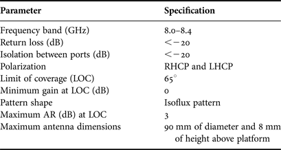
The requests in high data rate for future nanosatellite missions are incompatible with a telemetry application in VHF or S bands contrary to the X-band. The future antennas will have to present both isoflux radiation pattern and circular polarization (CP). Unfortunately, these two characteristics are often discordant. Several solutions have been previously designed by our laboratory. A trade-off between isoflux pattern quality and antenna size was made in [Reference Arnaud, Duchesne, Elis, Fouany, Monediere and Thevenot1–Reference Fouany3]. Whatever the design, the CP was limited to a single polarization. The main goal of this study is to design a dual circularly polarized isoflux antenna (DCPIA) for nanosatellite applications. The simultaneous use of this dual CP will increase the data rate. This antenna will be positioned above a 3U nanosatellite platform (100 × 100 × 300 mm3). Table 1 presents the antenna performances targets. They are set as objectives but not as definitive specifications. Usually, the choke horn antenna is a good way to perform an isoflux radiation pattern [Reference Geyer4–Reference Brachat8]. Without considering their dimensions, a dual circularly polarization and a good isolation between ports are ordinarily obtained using a septum and an orthomode transducer [Reference Davis, Digiondomenico and Kempic9, Reference Cano, Tribak, Hoyland, Mediavilla and Artal10]. Unfortunately, their physical size is not compliant with a nanosatellite application.
Table 1 Antenna performances target

Planar solutions such as an array of patches [Reference Maldonadoa, Panduroa, del Rio Bociob and Mendez11–Reference Roy and Balbin16] are interesting but they suffer from important dimensions and they require a complex feeding network. The proposed original solution is the association between a patch, used as feed, and a choke horn antenna, which is based on [Reference Arnaud, Duchesne, Elis, Fouany, Monediere and Thevenot1]. The first one provides the dual CP, while the latter allows realizing the isoflux radiation pattern.
Several authors have already conceived dual circularly polarized with patch antennas. Some of them [Reference Boyon, Bo, Nikolaou, Young-Sik, Papapolymerou and Tentzeris17–Reference Yi-Fan, Chun-Hsien, Lai and Fu-Chiarng20] used active components such as PIN diodes to create CP. This solution requires one or several DC bias control. It is not able to do the simultaneous polarization. Some other solutions exploit the even and odd modes in a coplanar waveguide transmission line or use a branch line coupler to create CP [Reference Narbudowicz, Xiulong and Ammann21–Reference Bai, Liang, Li, Zhou, Geng and Jin26]. All these designs limit the antenna miniaturization and the realization easiness. Therefore, in this work the initial feed is based on another solution proposed by Aloni and Zhang [Reference Aloni and Kastner27, Reference Zhang, Chen, Jiao and Zhang28]. It is made of a cross-shaped slot in a ground plane, which provides a coupling between a patch and a single ring microstrip line. This paper is organized as follows. Section II is a brief reminder of the compact choke horn antenna. Section III describes the feed optimization (using CST Microwave Studio) to reach the desired antenna characteristics over the entire frequency band. This section also deals with the association with the compact choke horn. The comparison between retro-simulations and measurements is presented in Section IV. Finally, a conclusion is given.
II. REMINDER ON THE COMPACT HORN ANTENNA
The already studied design for the choke horn antenna [Reference Arnaud, Duchesne, Elis, Fouany, Monediere and Thevenot1] is reminded in Fig. 1. The radiation patterns present an isoflux shape over the whole frequency band, but the maximum gain is obtained for an elevation angle θ gm = 35° instead of the expected limit of coverage (LOC) when the mechanical constraints are taken into account. The antenna radiates a mono CP with an axial ratio (AR) almost lower than 3 dB at the LOC whatever the azimuth angle (φ). The work in this paper aims to improve this design in order to conceive a dual circularly polarized antenna.
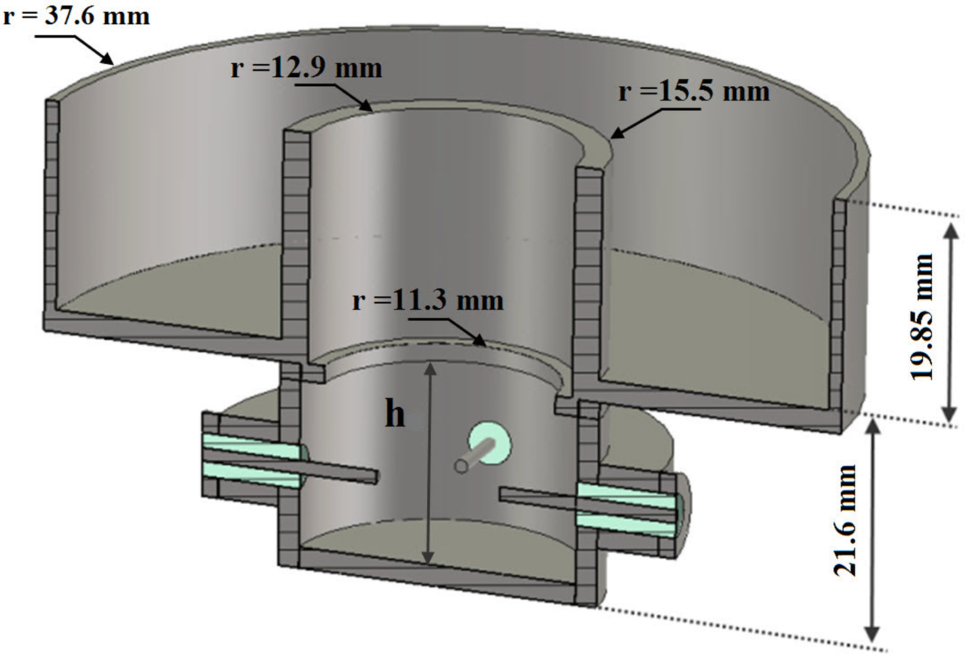
Fig. 1. Definition of the compact choke horn antenna.
III. ANTENNA DESCRIPTION
A) Description of the structure
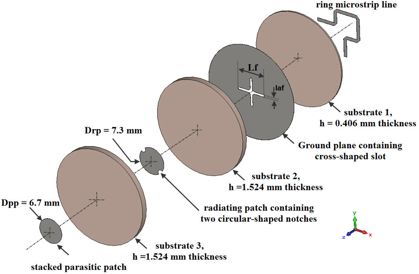
DCPIA (Fig. 2) is obtained by the addition of a dual circularly polarized patch feed (DCPPF) placed on the choke horn aperture (grayed area). The patch replaces the radiating aperture achieved by the waveguide of the antenna designed in [Reference Arnaud, Duchesne, Elis, Fouany, Monediere and Thevenot1]. Note that the dimensions of this horn have not been changed except the choke height. Indeed, the patch is excited at the center of the antenna and its radiating pattern is transformed by the interaction with the choke, i.e. by reducing this field at the center of the aperture. To provide a null of the aperture field, the radial position and the height of the choke ring are optimized. This optimization depends to the amplitude of the feed aperture field at the center. Since this parameter is similar between the patch and the radiating aperture, the optimization made in [Reference Arnaud, Duchesne, Elis, Fouany, Monediere and Thevenot1] remains correct. On the other hand, the choke height is not uniform (h 1 < h 2 = 19.85 mm) to have a realized gain (RG) >0 dB at the LOC whatever the frequency. Notice that one of the aforementioned value is still identical to the design in [Reference Arnaud, Duchesne, Elis, Fouany, Monediere and Thevenot1]. The set is inserted into the 3U platform, which is simulated as a perfect electric conductor cube but only with a height of 30 mm to reduce the simulation time.
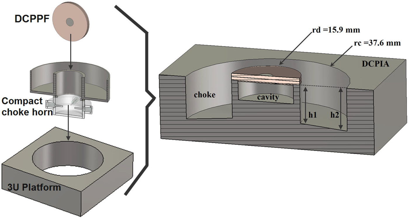
Fig. 2. DCPIA mechanical assembly.
The first step toward the goal is to find the best way to realize the feed of DCPIA (Fig. 3).

Fig. 3. Exploded view showing individual layers of the DCPPF.
B) DCPPF design
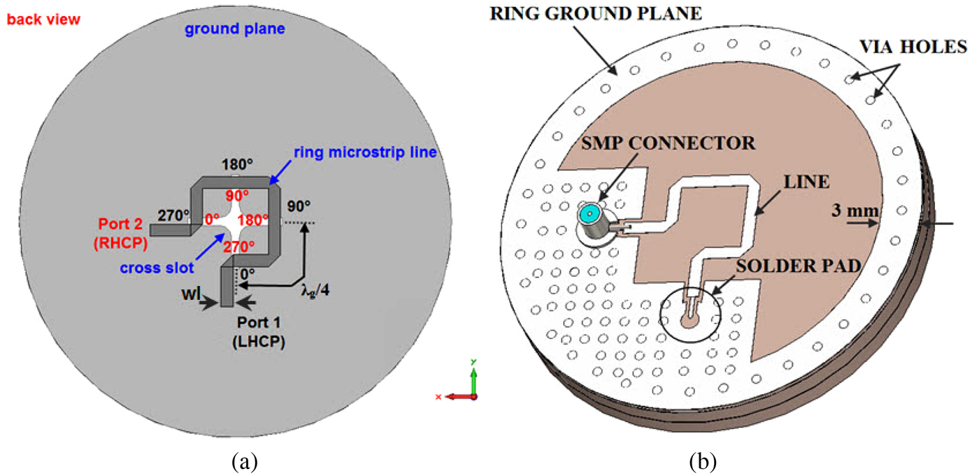
The feeding part of this antenna is obtained using a cross-shaped slot and a 50 Ω ring microstrip line (wl = 0.91 mm) respectively etched on the top and bottom of the Duroid 4003C laminate (substrate 1). The CP is obtained by a sequential phase feed of the slot (Lf = 7.4 mm, laf = 0.5 mm). Port1 produces a left circular polarization (LHCP) while Port2 creates a right circular polarization (RHCP). It is necessary that the microstrip line length between each slot branch corresponds to a 90° phase difference, i.e. a quarter of the guided wavelength (Fig. 4(a)). The radiating patch part of the antenna is made of two stacked patches. The lowest one is printed on a Duroid 4003C laminate (substrate 3). It includes two circular-shaped notches to improve the LOC AR whatever the azimuth angle (φ). The upper patch, which is etched on the top of this same substrate is useful for increasing the isolation bandwidth between both circularly polarized waves. Last substrate (substrate 2) without metallization is identical to the substrate 3 and it is sandwiched between the two other substrates. Firstly, this structure has been optimized in order to obtain the best electromagnetic performances taking into account mechanical constraints. Secondly, the whole antenna has been simulated on the 3U platform. The electromagnetic characteristics are almost identical except the radiation pattern (conventional patch radiation pattern to isoflux radiation pattern). A cylindrical cavity below the patch feed is created to reduce the DCPIA back radiation due to the slot [Reference Zhang, Geng, Zhou, Liang and Jin29].

Fig. 4. Ring microstrip. (a) Sequential phase feed. (b) Realization.
IV. MEASUREMENT AND SIMULATION VALIDATION
A) Realized structure
1) DCPPF REALIZATION
Figure 4(b) shows the DCPPF realization (back view). Two SMP-M-type coaxial connectors are soldered to each input of the 50 Ω microstrip line. An adapter SMP-F to SMA-F is connected during measurement. A ring ground plane and via holes are realized to improve the electrical continuity between the 3U platform, the ground plane and the transition SMP/microstrip line. The three printed circuits have been realized in our laboratory with a Circuit Board Plotter and have been assembled by Loctite glue. This last one and the adapters are not taken into account in the simulation. This etching method often involves a substrate thickness decrease where the metallization is removed (in our cases, 1.48 mm instead 1.524 mm for substrates 2 and 3). A retro-simulation was made to take into account all these remarks without optimizing again some parameters such as the slot length.
2) MANUFACTURED DCPIA
Figures 5(a)–5(d) show the manufactured DCPIA. An aluminum thin sheet allows simulating the 3U platform and reducing the interferences of the antenna test range interface.

Fig. 5. Ring Manufactured DCPIA. (a) Drawing perspective view. (b) Top view photography. (c) Left view photography. (d) Photography of the DCPIA positioned on our antenna test range support.
B) Comparison between measurements and simulations
1) RETURN LOSS AND ISOLATION
Figure 6(a) presents the simulated and measured return loss of the two ports. The experimental return loss of each port is higher than the predicted one. This discrepancy is probably due to the SMP connectors soldering. However, this level is below – 19 dB over a 400 MHz bandwidth. Figure 6(b) shows the isolation between the ports. A −12 dB isolation is almost obtained between 8.0 and 8.4 GHz. This isolation is below −20 dB between 8.15 and 8.35 GHz.
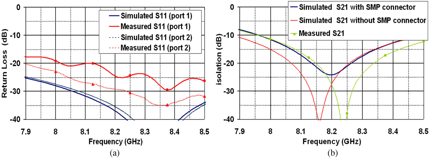
Fig. 6. [S] parameters. (a) Return loss. (b) Isolation.
2) DIRECTIVITY, RG, AND TOTAL EFFICIENCY
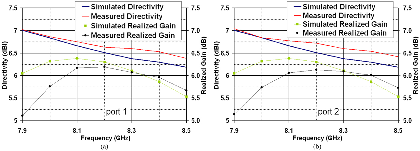
Figure 7(a) shows the comparison between the simulated and the measured directivity and maximum RG for the port 1. A satisfactory agreement is observed between these two results. It is the same for the port 2 (Fig. 7(b)). A slight discrepancy appears which probably results from a 50 MHz frequency shift of the isolation and the SMP/SMA adapter losses. Figure 8 shows that the total efficiency of DCPIA is identical to the feed one despite the presence of the horn. Excellent numerical results have been obtained with a total efficiency upper than 90% on the 8.0–8.4 GHz frequency band. The total efficiency measurement would have been close to 90% if no frequency shift appears in the isolation.

Fig. 7. (a) Directivity and maximum RG of port 1. (b) Directivity and maximum RG of port 2.
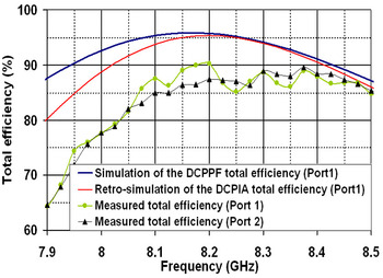
Fig. 8. Simulated and measured total efficiency.
3) RADIATION PATTERN AND AR
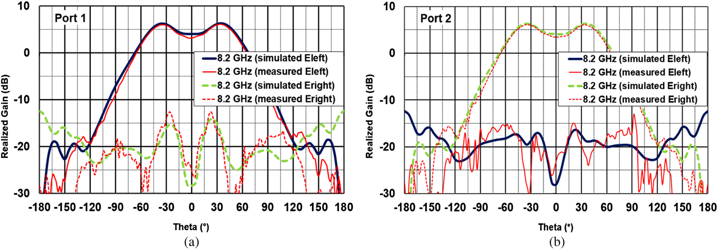
Figures 9(a) and 9(b) show the comparison of the simulated and measured RHCP and LHCP radiation patterns of the ports 1 and 2 at the central frequency (8.2 GHz) (RG drawn in the φ = 0° cut-plane). An isoflux shape is obtained on the frequency band, but the RG is maximum at the θ gm = 35° angle instead of 65°. This was the same for the antenna studied in [Reference Arnaud, Duchesne, Elis, Fouany, Monediere and Thevenot1]. The RG is close to 0 dB whatever the azimuth angle (φ) and the port.

Fig. 9. LHCP and RHCP radiation patterns (φ = 0° plane). (a) Simulation and measurement of port 1. (b) Simulation and measurement of port 2.
The measured AR radiation patterns (plane φ = 0°) and AR at θ = 65° versus azimuth angle (φ) are close to the simulated ones Figs 10(a) and 10(b). This characteristic almost meets to the antenna targets. This result would have been almost the same with other cut planes or frequencies.

Fig. 10. LHCP AR patterns (φ = 0° plane). (a) port 1 ; (b) port 2. AR at θ = 65° versus azimuth angle ; (c) port 1 ; (d) port 2.
Table 2 presents a comparison of measured and simulated antenna performances. All the specifications are obtained except the isolation and the LOC.
Table 2 Comparison of Antenna performances

V. CONCLUSION
This paper completes the previous work on circularly polarized isoflux antenna for nanosatellite applications. The proposed design allows a dual CP of this antenna. A very good agreement between simulation and measurement is obtained even if the −20 dB desired isolation is not satisfied in all bandwidth (2.4% instead 5%). The result can be improved by increasing the patch substrate thickness and by reducing the dielectric constant as shown in paper [Reference Zhang, Geng, Zhou, Liang and Jin29].
 Eric Arnaud was born in France in 1970. He received the Diplôme D'Etudes Supérieures Specialisées (DESS) and Ph.D. degrees in Electronics and Telecommunication from the University of LIMOGES in 1994 and 2010, respectively. He did his Ph.D. on circularly polarized EBG antenna. From 1996 to 2001, he has been in charge of the Microwave part of Free-Electron Laser (L.U.R.E). Since 2001, he has been in charge of XLIM laboratory's antenna test range. He participated in several research projects related to the design, development, and characterization of antennas. His research interests are mainly in the fields of circularly polarized EBG antenna, agile electromagnetic band gap matrix antenna, and isoflux pattern antenna.
 Cyrille Menudier was born in France, in 1981. He received the M.Sc. in High-Frequency Telecommunications from the University of Limoges and the Engineer degree from ENSIL in Electronics in 2004. He received his Ph.D. in Telecommunications from the XLIM Research Laboratory, University of Limoges, in 2007. He then got a post-doctoral position in CNES (French Space Agency), Toulouse, until 2009, where he worked on reconfigurable reflectarray antennas. He is currently an Associate Professor in the Antennas & Signal Team – RF Systems Axis of the XLIM Research Laboratory. His research interests include reconfigurable antennas, phased arrays, reflectarrays, parasitic element antennas, and mutual coupling effects.
 Jamil Fouany was born in Lebanon, in 1989. He received the Master's degree in Electronic and Optical Engineering for high-frequency communications (IXEO) from the University of Limoges, France in 2012. He is currently toward the Ph.D. degree in High-Frequency Communications, Photonics and Systems in the XLIM Laboratory, University of Limoges. His research interests include parasitic antennas with circular polarization.
 Thierry Monediere was born in 1964 in Tulle (France). He obtained his Ph.D. in 1990 in the IRCOM Laboratory of the University of Limoges. He is actually the head of department “Waves and Associated Systems” of Xlim laboratory and Professor with the University of Limoges. He develops his research activities in Xlim Laboratory (UMR CNRS/University of Limoges). He works on multifunction antennas, EBG antennas, and also on active antennas.
 Marc Thevenot was born in Limoges, France, in February 1971. He received the B.S. and M.Sc. degrees in Microwaves from the University of Limoges, France, in 1995. He received the Ph.D. degree in Electronic from the University of Limoges in 1999. He joined the CNRS in 2001. He is responsible of multifunction antennas activities in the “Waves and Associated Systems Department of Xlim”. His main current research activities deal with the electromagnetism, EBG antennas, materials, parasitic element antennas, reconfigurable antennas, and reflectarray antennas.