


I. INTRODUCTION
This paper presents the research done at LAAS-CNRS in the context of French National Agency Project “NANOCOMM”. This project aims to demonstrate the potential of nanotechnology for the development of reconfigurable, ultra-sensitive, low power consumption, and easy installation sensor networks with high performance in terms of reliability in line with the requirements of aeronautics and space. The main application is the Structure Health Monitoring for the aircrafts. Structure health monitoring (SHM) becomes a very important issue nowadays [Reference Stolz and Neumer1, Reference Young, Haugse and Davis2]. The deploying of a whole sensor network on the structure of the aircraft is necessary. It is estimated that there are around 20 000 aircrafts in activity and this number has to double by the end of 2025 and more than 1000 sensors are necessary for each one. The facility of sensor deployment also becomes a main issue.
The introduction of sensor network for structure health monitoring will improve the maintenance system and will lead to safer aircrafts, which is another major topic together with eco-efficiency and also to lower airplane ticket cost for passengers. Today the deployment of the sensors is limited by wired connections which lead to excess weight and carburant consumption. The wired sensors put also a huge problem of installation. The wireless solution, wireless sensor network, is imposed by these major constraints.
Each node of the sensor network is composed of nano-sensors, ultra-wide-band (UWB) transceiver and planar antenna. In this project, three-dimensional (3D) heterogeneous integration of these different components, on flexible polyimide substrate, is planned. The innovation proposed in “NANOCOMM” project is the use of 60 GHz frequency band for very short-distance instrumentation in areas with access difficulty and particularly in non-planar areas. As shown in Fig. 1, in the SHM application a lot of nodes have to be deployed in a limited, close area, the aircraft cabin, the 60 GHz band frequency is well suited because of short-range propagation which will limit the interferences between communicating nodes.
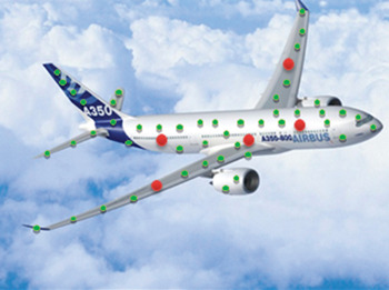
Fig. 1. WSNs deployed on the structure of the aircraft.
The paper is structured as follow. In Section II, the description of the 60 GHz communicating nodes is done. In Section III, the polyimide material choice is discussed and the technological process choices for mounting the transceivers on the flexible substrate are presented. Section IV is dedicated to the flexible assembly technological process and of the characterization of the early-realized prototypes.
II. DESCRIPTION OF THE COMMUNICATING NANO-OBJECT
From the system integration point of view, the research work presented here aims at assembling different components of the communicating node (as shown in Fig. 2): nano-sensors, the 60 GHz UWB transceiver (IR-UWB digital baseband, 60 GHz front-end), and E/R antenna. The main constraint concerns the packaging of the transceiver. The communicating node has to be seen as a modular platform that can include different kinds of sensors. For this purpose, an innovative solution will be developed.
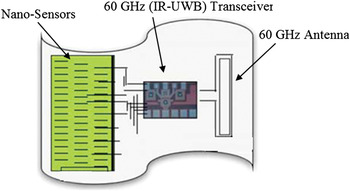
Fig. 2. Architecture of the communicating Nano-Object.
To guarantee very low-power transceivers and low interferences, we used UWB Impulse Radio (IR-UWB) communications. The low-power millimeter-wave front-end circuits design is enabled by the use of CMOS nanotechnology. Details of the different components, selected for this project, are given in the following sections.
A) The nano-sensors
The sensor can be realized directly on the flexible substrate or on silicon and then reported on the flexible substrate. Different kinds of sensors can be integrated on this substrate, as strain gauge [Reference Ressier, Palleau, Garcia, Viau and Viallet3], crack wire, or chemical/humidity detection sensor [Reference Temple Boyer, Benyahia, Sant, Pourciel-Gouzy, Launay and Martinez4].
B) The transceiver
1) 60 GHZ RECEIVER IN CMOS 65 NM TECHNOLOGY
Figure 2 shows the die photograph of the fabricated receiver frontend [Reference Kramer, Dragomirescu and Plana5]. Its very small size of 0.550 mm2 is essentially pad-limited: the aligned circuit blocks without pads are only about 200 µm wide. This is the result of using a total of 17 compact spiral inductors for matching.
The number of pads can further be reduced because multiple VDD and ground connections are provided (see the respective symbols in Fig. 3). These redundant connections are not essential for the operation of the receiver due to its low-supply current (about 43 mA). Furthermore, the bias voltages could be derived from voltage drain drain (VDD) in a redesigned version, allowing removing four more pads. The lower part of the circuit, which consists of the differentially implemented parts, is very symmetric to reduce mismatch and improve local oscillator-to-baseband (LO-to-BB) isolation.
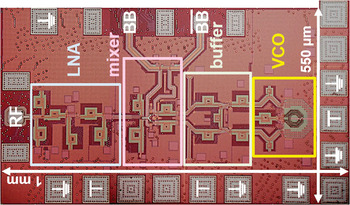
Fig. 3. Microphotograph of the fabricated CMOS receiver front-end.
The receiver front-end was characterized on-wafer using a 67 GHz single-ended 100 µm G-S-G Picoprobe to provide the RF signal and a differential G-S-G-S-G probe of the same type to measure the BB output. The DC voltages were connected using two eyepass six-finger probes.
The measurements were done using either an Anritsu MS4647A 70 GHz VNA to obtain the return loss. In this case, one of the differential BB outputs was matched to 50 Ω by a precision load. For conversion measurements, an Agilent E8257D 67 GHz synthesizer served as signal source and a LeCroy SDA813Zi 13 GHz real-time oscilloscope with spectrum analyzer functionality was connected to the circuit's differential BB output. The loss due to cable and probes is de-embedded and 3 dB is added to the output power in the case of single-ended measurements.
The receiver front-end is biased at the optimum current densities of the circuit components by applying bias voltages of V bias1 = 460 mV, V bias2 = 390 mV, V bias3 = 510 mV, and V bias4 = 540 mV. It draws about 43 mA from a 1 V supply, thus consuming P DC = 43 mW. This power consumption can be reduced by the amount contributed by the BB buffers in an integrated version, because the BB output usually does not have to drive two 50 Ω loads but a variable gain amplifier with high-impedance inputs. Thus, voltage-controlled oscillator (VCO), LO buffers, downmixer, and low noise amplifier (LNA) together consume only 29 mW.
This receiver is realized in 65 nm technology and will be reported on the substrate using the flip-chip technique.
2) 60 GHZ TRANSMITTER IN CMOS 65 NM
The transmitter is built in CMOS 65 nm Bulk technology (Fig. 4). The block is designed to achieve low-power dissipation and maximum power output in the same time. A fully differential architecture is adopted to minimize the common mode and common noise in chain. The frequency translation is obtained by a direct up-conversion from DC to 60 GHz band. The transceiver employs a voltage-controlled oscillator (VCO) [Reference Kraemer, Dragomirescu and Plana6] with a Colpitts configuration. The mixer is a ring passive mixer composed by four transistors each one with a size of 50 µm. This size is designed to achieve the minimum conversion loss and the maximum value of output −1 dB compression point as well. A high-performance transformer balun was designed and measured [Reference Ercoli, Kramer, Dragomirescu and Plana7], and is employed in our transmitter architecture to transform the differential signal into single-ended RF output. A series of Cascode buffers are placed in the chain: the first one, between the VCO and mixer to increase the value of local oscillator power until the request value of 0 dBm, and the others are placed at the RF output of the mixer to compensate for the losses of the frequency converter. The performances simulated for the transmitter are: +5 dB of gain, 1 dBm of −1 dB compression point (CP) and 52–67 GHz RF bandwidth with only 50 mW.
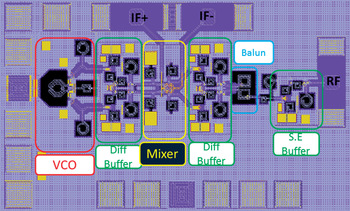
Fig. 4. Microphotograph of the designed CMOS transmitter front-end.
3) 60 GHZ PATCH ANTENNA
Millimeter-wave antennas are naturally an essential component of such applications. To offer more flexibility of such communication systems at such high frequencies while ensuring low-cost fabrication processes and reliable components, the use of low-loss flexible substrates has become a natural challenge seeking low-loss, light-weight conformal antennas, and short-range front-end modules. In this work, 60 GHz rectangular patch antennas are designed fabricated and measured on a flexible 127-µm-thick polyimide substrate. More details are given in Section IV.
III. TECHNOLOGY AND MATERIAL SELECTION
As described in the previous section, each component has its own specific constraints. For the nano-sensors, we have constraints of roughness, mechanical, and dielectric properties. Regarding the transceiver, we have to take into account the flip-chip process, the thermal properties, and the 60 GHz interconnections. Finally, the antenna adds constraints in terms of RF properties, substrate thickness, and metallization properties. Hence, the challenge, here, deals with the choice of the flexible substrate, the technology, the pads materials, and the interconnection architecture to minimize the RF losses and the parasitic effects. Based on these criteria, two solutions can be investigated: the first is to achieve a postponement of the different components on a same flexible substrate. But this solution requires a significant improvement of the surface state. The second solution consists of the realization of the nano-sensors on a flexible substrate first. Then, the transceiver and the antenna are added on a second substrate. For the research work presented in this paper, the second solution is selected. This solution is conducted in two steps: in the first one, the material choice and the technological process validation are performed. In the second step, integration tests are realized.
Our choice goes to a polyimide flexible substrate called Kapton because of its good thermal and RF properties. The permittivity of Kapton is 3.2 and loss tangent tan ± = 0:002 which allow us to expect a good behavior at 60 GHz. The thickness of 127 µm is imposed by the antenna design. In fact, the antenna is composed of a top side on which a square patch is printed. The bottom side is used as ground plane. Hence, to have a good radiation pattern, a thickness of 127 µm is needed.
IV. PROTOTYPE FABRICATION AND CHARACTERIZATION
In this section, the fabrication process and the first prototype characterizations are described. The technological process used for the realization of Kapton circuits is presented. The principal difficulty consists of the flexible film handling and its use in the photolithography equipment, vacuum deposit, and chemical etchings. To overcome this difficulty, we use a four-inch silicon wafer as a host support. The critical obstacles consisted of finding a way to adhere the polyimide film on this Si support. This adhesion has to be compatible with the various technological stages (vacuum, solvent, and temperature) and allows after manufacture a peeling without any physical or chemical constraint. The manufacturing process developed here is composed of various stages of evaporation metallization and photolithography for structuring the conduction lines as well as the electric insulation. The parameters of the various stages were optimized to guarantee the flexibility of the film.
Non-destructive flow detection means, RF, and electrical interconnections tests are used to ensure that the flip-chip step is done properly. More details are given in the following sections.
A) Fabricated structures
To realize Kapton circuits, the following process is adopted (see Fig. 5): first, a polymer spin coating is performed for the adhesion of the polyimide on the holding wafer. Second, polyimide was patterned on the substrates by lamination. For this step, the used polyimide film is ‘Kapton’ type with a thickness of 127 µm. Third, resin lift spin coating is realized. Fourth, a photolithography is done for the conduction lines placement. The metallization is realized by lift-off. Finally, a passivation layer is deposited.
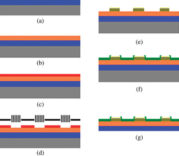
Fig. 5. Processing methods for copper circuits: (a) polymer spin coating for the adhesion; (b) polyimide lamination; (c) resin lift spin coating; (d) photolithography; (e) metallization resin stripping by lift-off; (f) passivation layer; and (g) substrate peeling.
Figure 6 shows the photograph of fabricated test circuit on Kapton. Good resolution is obtained for the circuit pads.

Fig. 6. Microphotograph of the fabricated circuits on Kapton.
Given the cost of chips made with 65 nm technology, dummy chips were also fabricated. These chips have the same access (pads dimensions and placement) as real transceivers. These dummies are used for interconnection tests and are composed of high-resistivity silicon substrate on which aluminum lines are deposited and pads passivation is performed.
These dummies are reported on the flexible Kapton substrate using the flip-chip technique. Usually, the flip chip is suited for the ceramic substrates regarding the viewpoint of performance and ease of assembly. Flatness and low thermal expansion coefficient (coefficient of thermal expansion (CTE)) are two preferred attributes for flip-chip substrates that are inherent in most ceramics. However, reliability can be regained and joint stress can be reduced using flip-chip under-filling processing. Moreover, Kapton polyimide substrate is noted for good high-temperature performance (zero strength factor at high temperature), a property usually confined to ceramics. Thus, Kapton film is well suited for use as chip carrier and flip-chip assembly substrate.
There are three steps in making flip-chip assemblies of the dummies on Kapton substrate: bumping the dummies, attaching the bumped dummy to the flexible substrate and filling the remaining space under the dummy with an electrically non-conductive material. The bump serves several functions in the flip-chip assembly [Reference Riley8]. Electrically, the bump provides the conductive path from chip to substrate. The bump also provides a thermally conductive path to carry heat from the chip to the substrate. In addition, the bump provides part of the mechanical mounting of the die to the substrate. Finally, the bump provides a spacer, preventing electrical contact between the chip and substrate conductors. A modified standard wire bonding technique is used in the gold stud bump flip-chip process. Wire bonders are modified to break off the wire after attaching the ball to the dummy bond pad. Figure 7 shows a gold stud bump on a bond pads. The bump diameter at the base is about 55 µm. The wire-bonding tool presses the gold bump against the aluminum bond pad, applying mechanical force, heat, and ultrasonic energy to create a metallic connection. The gold ball, or “stud bump” remaining on the bond pad provides a permanent connection through the aluminum oxide to the underlying metal.
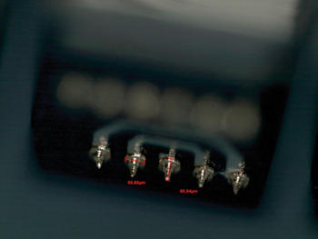
Fig. 7. Ni/Au stud bumps on aluminum pads of the dummy chip.
The dummies are ready to be reported by the flip-chip technique on the Kapton flexible substrate.
B) First assembly tests
In the final stage of assembly, the under-chip space is filled with a non-conductive “underfill” adhesive joining the entire surface of the chip to the substrate. The underfill is needle-dispensed along the edges of each chip and it provides additional mechanical strength to the assembly. Figure 8 shows the first assembly tests of an LNA [Reference Kramer, Dragomirescu and Plana9] dummy on Kapton.
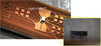
Fig. 8. Photograph of the first assembly tests and cross-section view of the mounted dummy.
Figure 9 shows bottom view of a daisy chain dummy mounted using the flip-chip technique. We can verify that all bumps are connected correctly. The “underfill” can be observed and is drawn into the under-chip space by capillary action and heat-cured to form a permanent bond.
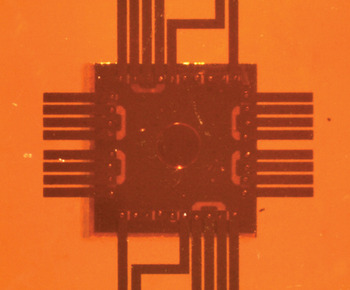
Fig. 9. Bottom view (through Kapton) of a daisy chain mounted by the flip-chip technique.
The flexible substrate with the mounted components can thus be cut using simple chisel and packaged in 3D. The connection of this flexible substrate to another substrate is done by an anisotropic electrically conducting adhesive that ensures an excellent flexibility. Characterizations during the processes and functional tests made it possible to validate the process developed here.
C) Characterizations
After the assembly process, the components follow different kinds of tests. In the first step, non-destructive flaw detection means are used to check if all the bumps are connected properly and that there is no breaking problem between the chip and substrate. These tests help to identify failed parts of the assembly. RF tests and tests to characterize the bumps resistivity are also done (Daisy chain, four-probe method). As shown in Fig. 10, on wafer impedance measurements are performed to determine bumps contact resistance. A resistance of 15 mΩ is measured for the bumps.
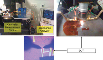
Fig. 10. On wafer impedance measurement bench.
Different components have been designed and realized at 60 GHz on a flexible substrate. A classical rectangular patch antenna is first designed (see Fig. 11). A simple gap coupled resonator is also designed to characterize precisely the dielectric permittivity and loss tangent at the design center frequency.
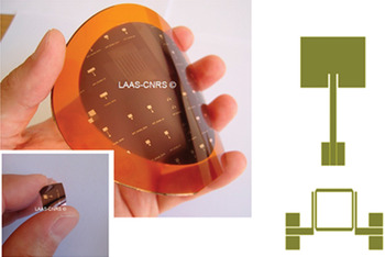
Fig. 11. Photograph of different fabricated components (60 GHz resonator and path antennas).
A Suss-Microtech Probe Station with 67 GHz probes and 110 GHz Anritsu Vector Network Analyzer were used to measure the “S-parameter” of the fabricated patch antennas.
Preliminary results for the measured reflection coefficient of the latter antenna are shown in Fig. 12.
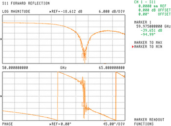
Fig. 12. Measured reflection coefficient of the fabricated 60 GHz patch antenna.
Figure 13 shows a photograph of a solid-state battery mounted on Kapton. This battery is connected on the same Kapton substrate as the different others components and it serves to supply power to the transmitter/receiver and the sensors data processing circuits.
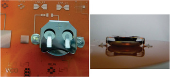
Fig. 13. Photograph of the solid-state battery mounted on Kapton.
An improved battery contact assembly on the flexible substrate is demonstrated. The electric connections are done by two ways. In the first way, the flex pad is connected to a battery rack using an electrically epoxy glue. This technique can be done by a simple pick and place. The temperature of the glue polymerization is less than 80°C. Then we can insert a standard flat battery on it. In the second way, electric connections are done using a refillable thin battery that is connected to the flex by anisotropic conductive film. The integration of the energy cell allows us to produce autonomous sensors.
V. CONCLUSION
Flexible circuit technology opens doors to new opportunities for engineers and system designers to make a complete transition to the 3D interconnection. Flexible circuits are obviously unique among electronic packaging technologies to offer a wide variety of solutions where compactness and heterogeneous integration of different components on the same substrate, are needed. In this paper, the very first and unique results presenting the potentials of flexible substrate for the heterogeneous integration of communicating Nano-Objects are presented. The choice of the technological process (selection of materials and choice of process technology) has been discussed. The design and fabrication of test structures for the verification of the RF interconnections quality have been made. As detailed in Section IV, gold stud bump flip-chip forms connections from die pads to the flexible substrate by means of gold bumps placed on each bond pad in a process similar to gold wire bonding. Gold stud bumps require no under-bump metallization (UBM) or special wafer treatment before bumping. The developed process allows a 3D assembly on flexible substrates simple, collective, and low cost. To increase implementation of new SHM technology, our proposal focus on an integrated approach where sensors, transceivers, and antennas can be co-located together on the same flexible support that can be easily deployed everywhere on the aircraft structure. Future works will address the characterization of the realized structures under real working conditions. Real case applications (on aeronautical composite components) are being investigated by the authors to bring a proof-of-exploitation of these new wireless nano-sensor nodes.
ACKNOWLEDGEMENTS
This work was supported by the French National Research Agency (ANR) in the frame of its program” Recherche Technologique Nano-INNOV/RT” (NANOCOMM project no. ANR-09-NIRT-00 4).
 Mohamed Mehdi Jatlaoui received the Diploma degree in Telecommunications engineering from the National Engineering School of TUNIS, Tunisia, in 2004. He received the M.S and Ph.D. degrees in Microwaves, Electromagnetism and Optoelectronic from the National polytechnic Institute of Toulouse respectively in September 2005 and April 2009. He is currently a research engineer with the CNRS-LAAS (French National Scientific Research Center – Laboratory of Analysis and Architecture of Systems) in Toulouse, France. He is interested in developing Wireless Passive MicroSytems (Microsensors) based on the Electromagnetic transduction principle for passive remote sensing. During his Doctoral studies, he acquired a theoretical and practical background dealing with such MicroSystems development (theory, Electromagnetic Modeling, RF design, EM Simulations, Fabrication process in LAAS-CNRS cleanroom, and on wafer antenna/RF/pressure measurements). His fields of interest include Wireless Interrogation Techniques based on FMCW Radar, integrated packaging for RF and wireless applications using organic flexible substrate, passive sensors, microwave microelectromechanical systems (MEMs), system-on-package (SOP), 3D heterogeneous integration of communicating nono-objects, integrated (multiband, conformal) antennas, and flexible electronics.
 Daniela Dragomirescu was born in Bucharest, Romania in 1972. She received the Electronics and Telecommunication engineering degree from Bucharest Polytechnic University, Romania in 1996 and her Ph.D. degree from the National Institute of Applied Sciences, Toulouse, France. She is an Associate Professor at National Institute of Applied Sciences, Toulouse and a researcher at Laboratory for Analysis and Systems' Architecture (LAAS-CNRS). Her main research interests are in Wireless Sensor Networks, system architecture and modeling, and digital and RF circuit design.
 Mariano Ercoli was born in Cascia Italy in 1982. He received the master's degree (Magna Cum Laude) at the University of Perugia, Italy in 2009. At present, he is a Ph.D. Student at LAAS-CNRS laboratory in Toulouse, France under the supervision of Associated Professor Daniela Dragomirescu and Professor Robert Plana. His research interests include the modeling, design, and testing of single chip millimeter wave circuits in CMOS technologies for Ultra Wide Band applications.
 Michael Kraemer was born in Bad Mergentheim, Germany, in 1980. He received the Dipl.-Ing. (BA) degree from BA Mosbach, Germany, in 2003 and the Dipl.-Ing. degree from the University of Stuttgart, Germany, in 2007, both in electrical engineering and is currently working toward his Ph.D. degree at LAAS-CNRS in Toulouse, France. During his studies, he stayed one year at University of Massachusetts, Amherst, USA, and did internships at ebm-papst GmbH, DaimlerChrysler AG and Robert Bosch GmbH. His research interests include the design and modeling of millimeter-wave circuits. Mr Kraemer is a Fulbright fellow and the recipient of the 2007 VDE-award at the University of Stuttgart.
 Samuel Charlot is born in 1979. He received the master's degree in Materials and Micro Technology from the Var Institute of technology, Toulon, France in 2004. From 2004 to 2006, he worked on the development of microfluidics systems in LAAS-CNRS, Toulouse, France. In 2006, he worked in the packaging of oxygen sensor at Néosens, Labège, France. From 2007 to 2008, he worked on a low-cost technology for the integration of sensors silicon in polymer microfluidic systems in LAAS-CNRS, Toulouse, France. Since 2008, he has been working on packaging area and more specifically in screen printing technology and flip-chip interconnect technology in the team packaging in LAAS-CNRS, Toulouse, France.
 Patrick Pons received his “Doctorate” in electronics from Paul Sabatier University, Toulouse, France, in 1990. Since 1991, he is a researcher in the CNRS LAAS (National Scientific Research Center – Laboratory of Analysis and Architecture of Systems) in Toulouse. His research interests are focused in microtechnology and microsensors. In 1995, he started in the lab the study on microtechnology for microwave applications. Now he manages the development of this technology for high-frequency Microsystems and develops also pressure sensors for specific applications.
 Hervé Aubert was born in Toulouse, France, in July 1966. He received the Eng. Dipl. in July 1989 and the Ph.D. degree (with high-honors) in January 1993, both in Electrical Engineering and both from the “Institut National Polytechnique” (INPT), Toulouse, France. Since February 2001, Hervé Aubert is Professor at INPT. He has joined the “Laboratoire d'Analyse et d'Architecture des Systèmes,” National Center for Scientific Research, Toulouse, in February 2006. From April 1997 to March 1998, he was a Visiting Associate Professor at the School of Engineering and Applied Science, University of Pennsylvania, Philadelphia, USA. Dr Aubert is a contributor to the books Fractals: Theory and Applications in Engineering (Springer, 1999), Micromachined Microwave Devices and Circuits (Romanian Academy Edition, 2002), and New Trends and Concepts in Microwave Theory and Techniques (Research Signpost, 2003). He has authored or co-authored one book, 44 papers in refereed journals and over 120 communications in International Symposium Proceedings. He holds four international patents in the area of antennas. Dr Aubert is the Secretary of “IEEE Antennas and Propagation French Chapter” and was the Vice-Chairman of this Chapter from 2004 to 2009 and Secretary from 2001 to 2004. Dr Aubert is a senior member of IEEE (1999) and a member of URSI commission B.
 Robert Plana was born in March 1964 in Toulouse. He obtained his Ph.D. in 1993 at LAAS-CNRS and Paul Sabatier University on the Noise modeling and characterization of Advanced Microwave devices (HEMT, PHEMT, and HBT) that includes the reliability. In 1993, as associate professor at LAAS-CNRS, he has started a new research area concerning the investigation of millimeter-wave capabilities of Silicon-based technologies. More precisely, he has focused on the microwave and millimeter-wave properties of SiGe devices and their capabilities for low-noise circuits. In 1995, he has started a new project concerning the improvement of the passives on silicon through the use of MEMS technologies. In 1999, he was involved with SiGe Semi-conductor in Ottawa where he was working on the low-power and low-noise integrated circuits for RF applications. In the same year, he has received a special award from CNRS for his works on Silicon-based technologies for millimeter-wave communications. In 2000, he was professor at Paul Sabatier University and Institut Universitaire de France and he has started a research team at LAAS-CNRS in the field of Micro and Nanosystem for RF and millimeter-wave communications. Its main interests are on the technology, design, modeling, test, characterization and reliability of RF-MEMS for low-noise and high-power millimeter-wave applications, and the development of the MEMS IC concept for smart microsystems. He has built a network of excellence in Europe in this field “AMICOM” regrouping 25 research groups. He has authored and co-authored more than 300 international journals and conferences. In 2004, he was appointed as Deputy Director of the Information and Communication Department at the CNRS Headquarter. From January 2005 to January 2006, he was director of the Information and Communication Department at CNRS. Since 2006, he is heading a research group at LAAS-CNRS in the field of Micro and Nanosystems for wireless communications. From November 2007 to November 2009, he was the project officer of the National Nanotechnology Initiative at the “French research Agency”. Since November 2009, he has been the head of the department “Physic, Mathematics, Nanosciences & Nanotechnology, Information and Communication Technology” at the Ministry of research in charge of defining the French strategic for research and innovation.


