Introduction
With new developments in communication systems and remote-sensing techniques, the need for ultra-wideband antenna array is also increasing. In recent years, a new methodology to design an antenna array is proposed, in which, mutual coupling between the elements of antenna array is used to improve the performance of the antenna array. The theoretical concept of the infinite connected array was proposed by Wheeler in 1965 [Reference Wheeler1]. Based on Wheeler's current sheet concept, Munk realized a practical continuous current aperture array [Reference Munk2], where inter-digital capacitor between the dipole edges is utilized to counteract the inductive behavior of the ground plane to obtain wideband performance. A wideband low-profile antenna array using long-slot aperture based on current sheet array was proposed by Lee et al. [Reference Lee, Livingston, Koenig, Nagata and Lai3]. Later on, Lee et al. proposed a 10:1 wideband long-slot array with ferrite loaded ground plane [Reference Lee, Livingston and Nagata4]. A wideband wide-scan antenna array of connected dipoles was proposed by Cavallo et al. [Reference Cavallo, Neto, Gerini, Micco and Galdi5]. The array had 7 × 7 elements in which each element was fed with a loop-shaped transformer to avoid common-mode resonances. A wideband banyan tree antenna array has been proposed by Holland et al. [Reference Holland and Vouvakis6]. The array employs a modular, low-profile structure which is directly fed by an unbalanced line. Shorting pins are utilized in the array design to reduce the common mode resonance. Further, Holland proposed 16 × 16 elements dual-polarized planar ultra-wideband modular antenna array that comprised tightly coupled dipole array [Reference Holland, Schaubert and Vouvakis7]. Interwoven spiral array with a 10 : 1 bandwidth on a ground plane has been proposed by Tzanidis et al. [Reference Tzanidis, Sertel and Volakis8]. Wideband performance is achieved via enhanced coupling due to interwoven arms of the spiral. To model the radiation impedance of ultra-wideband antenna array with strong inter-element coupling, an equivalent circuit has been proposed by Alwan et al. [Reference Alwan, Sertel and Volakis9]. A low-profile compact tightly-coupled array of the patch antennas was proposed by Irci et al. [Reference Irci, Sertel and Volakis10] where, the inter-element capacitance was obtained by the close proximity of the patch antennas which resulted in a very low-profile structure. A wideband antenna array with tightly coupled octagonal ring elements has been proposed by Chen et al. [Reference Chen, Yang and Nie11] where capacitive coupling between the elements is realized by the inter-digitizing the end portions of the ring elements. An ultra-wideband, wide scanning tightly-coupled dipole antenna array with integrated balun has been proposed by Doane et al. [Reference Doane, Sertel and Volakis12] in which the reactance of the compact Marchand balun is utilized as a matching network for each element. Moulder et al. [Reference Moulder, Sertel and Volakis13] proposed a tightly coupled antenna array having a resistive frequency selective surface and a superstrate are utilized to enhance the performance of the antenna array. A wideband planner array with integrated feed and matching network with a non-symmetric tightly coupled dipole array has been proposed by Kasemodel et al. [Reference Kasemodel, Chen and Volakis14].
In various cases of the tightly-coupled antenna array, a large number of dummy elements are used to compensate for the edge elements performance. To enhance the performance of the edge elements, few techniques have been proposed. A method to design the excitation taper of finite size tightly coupled antenna array for efficient matching of all array elements has been proposed by Tazandis [Reference Tzanidis, Sertel and Volakis15]. Later, Tazandis proposed a low profile tightly coupled dipole array with an integrated balun in which different types of termination are used to enhance the performance of the finite array [Reference Tzanidis, Sertel and Volakis16].
Most of the arrays reported in the literature using tight coupling technique havea large number of elements. With the infinite array analysis, the design of the tightly coupled array is computationally fast but is not accurate for small finite arrays. A small array of connected long-slot antenna [Reference Awasthi and Harish17] was proposed having optimized length and width of the feeding microstrip line for each port to match it with 50 Ω input impedance. A 2 × 8 elements tightly coupled antenna array with conjugative elements of a column printed on the opposite layer of the dielectric substrate has been presented in [Reference Awasthi and Harish18]. Due to the dual layer structure, the fabrication process is very complex in [Reference Awasthi and Harish18].
In this paper, a wideband, low-profile, compact (2 × 8 elements) array of tightly-coupled dipole antennas are proposed. In the proposed array, the triangular lattice is utilized to reduce side lobe level in one of the planes. Dipole is printed on the same layer of the substrate therefore, it reduces the fabrication complexity in the proposed array. The proposed array is basically designed for fan-type beam applications. Due to that, only two columns are used in this design. Coupling due to near-field radiation of the dipole elements along with the capacitive coupling between edges of dipoles is utilized to achieve ultra-wideband impedance bandwidth in the proposed array. Effect of the feed network on the performance of the tightly coupled antenna array is also discussed in this paper. Feed network of the proposed array is placed below the reflector and shielded by a metallic enclosure to reduce its effect on the performance of the array.
Analysis and design of proposed array
A unit cell of the proposed array is illustrated in Fig. 1. The structure is infinite in the y-direction and finite along the x-axis. Due to the triangular lattice, four dipoles are required to form the smallest repeating entity to be used as the unit cell of the proposed array. Dipoles are printed on the top layer of a substrate (Taconic TLY-5 εr = 2.2) of thickness t. Length and width of the dipole are l d and w d, respectively. Excitation gap between the dipoles is g. Along the x-direction, the dipoles are placed such that there exists a spacing s between the dipoles in the same row and two rows are placed with an offset of d x. Inter-element spacing between the dipoles along the y-axis is d y. A metallic reflector is placed at a distance of h below the substrate (Fig. 1(b)). Balun for each dipole is printed on a FR-4 substrate and connected to the dipole. Detailed structure of the balun and its assembly with the dipoles are presented in the section “Feed Network Design”. Various dimensions of the unit cell are given in the caption of Fig. 1.
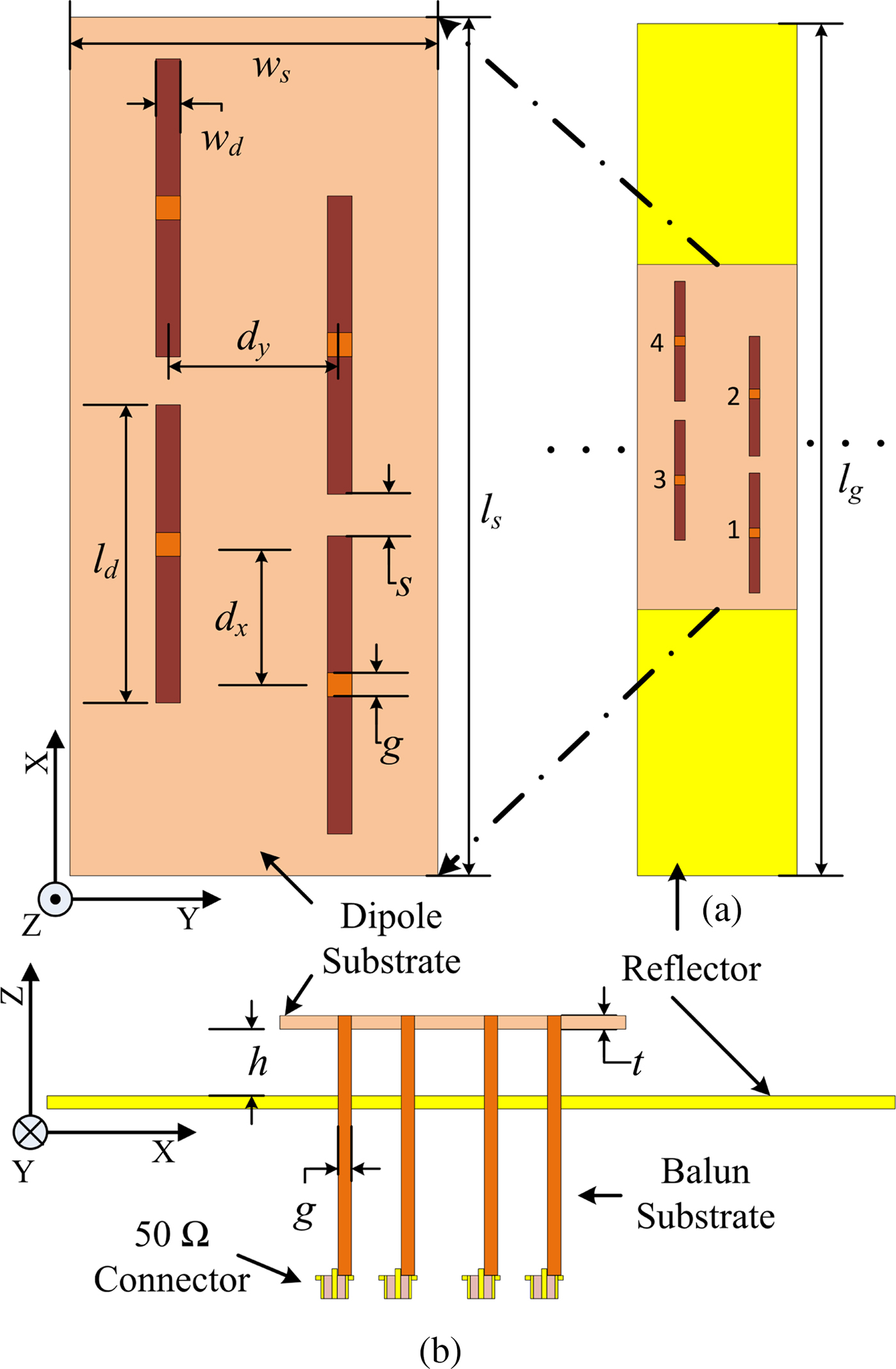
Fig. 1. Detailed geometry of the proposed unit cell, (a) Top view and (b) side view. g = 1.6, d y = 10.5, d x = 9, l d = 19, l g = 121, l s = 60.5, w d = 1.35, w s = 21, h = 6, s = 4, and t = 1.6. All dimensions are in mm.

Fig. 2. Reflection coefficient of the array elements for various configurations.
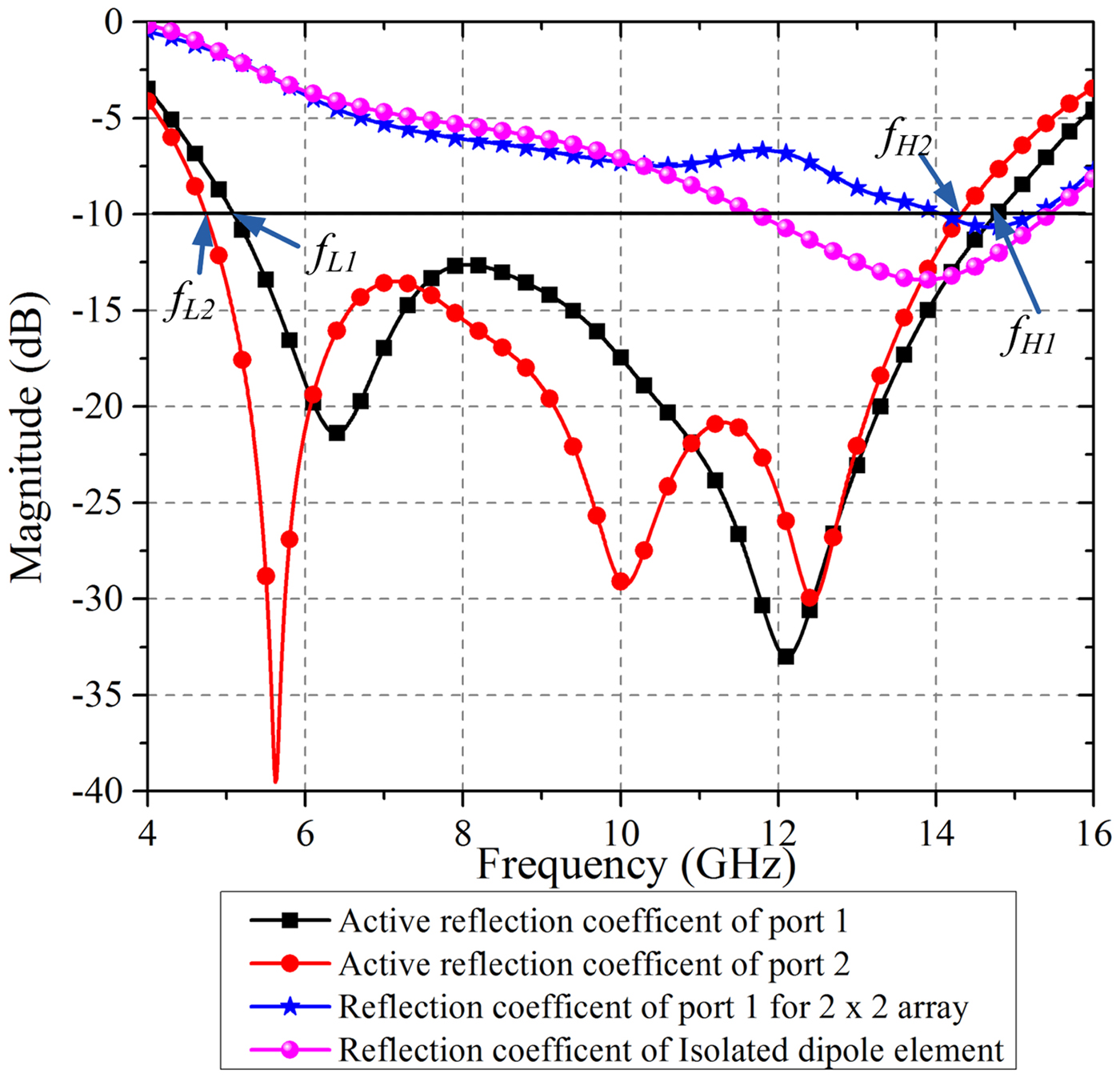
For the infinite array analysis, dipoles within the unit cell are excited simultaneously witha discrete port having source impedance of 175Ω. Balun is not used in this analysis. A comparison of the active reflection coefficient [19] of the elements of the unit cell, the reflection coefficient of element 1 of 2 × 2 finite array and the reflection coefficient of single isolated dipole element is shown in Fig. 8. In this paper, the reflection coefficient at the terminal of an element is computed or measured by terminating all other elements ina matched load and the active reflection coefficient is computed by exciting all other elements. Hence, the active reflection coefficient takes into account mutual coupling from all the elements and is more appropriate in case of the tightly coupled antenna array. Active reflection coefficient curves of port 3 and port 4 overlap with that of port 2 and port 1, respectively. It is observed from the unit cell results that the ultra-wideband input impedance bandwidth is achieved from simple dipole elements by utilizing high inter-element coupling.
Infinite array analysis
To analyze the behavior of the proposed array, a parametric analysis of the unit cell is carried out. Let f L1 and f L2 be the lower − 10 dB band-edge frequencies of the active reflection coefficient at port 1 and port 2, respectively. Similarly, f H1 and f H2 be the upper − 10 dB band-edge frequencies at port 1 and port 2, respectively. These band edge frequencies are marked in Fig. 8. Fig. 3 shows the variation of the lower and upper band edge frequencies with respect to various design parameters. Effect of variation in dipole length l d on the band edge frequencies is shown in Fig. 3(a). By increasing l d, the lower cut off frequencies are decreasing while there is almost no effect on the upper cut off frequencies. Thus, we can conclude that by increasing the dipole length, bandwidth of the proposed array can be increased. It is observed from Fig. 3(b) that by increasing dipole width w d, the upper band edge frequencies are increasing proportionally, while the lower band edge frequencies are unaffected, which also concludes that wider dipole gives wider impedance bandwidth. The feed gap also affects the upper band edge frequency more than the lower edge frequency. Lower value of feed gap results in wider bandwidth (Fig. 3(c)). Offset d x is used to create the triangular lattice in the proposed array. Effect of variation in d x is shown in Fig. 1(d). When there is no offset, i.e. rectangular lattice, the band edge frequency for port 1 and port 2 are same. Offset affects the band edge frequencies, but the bandwidth of the proposed array itself does not change with d x.
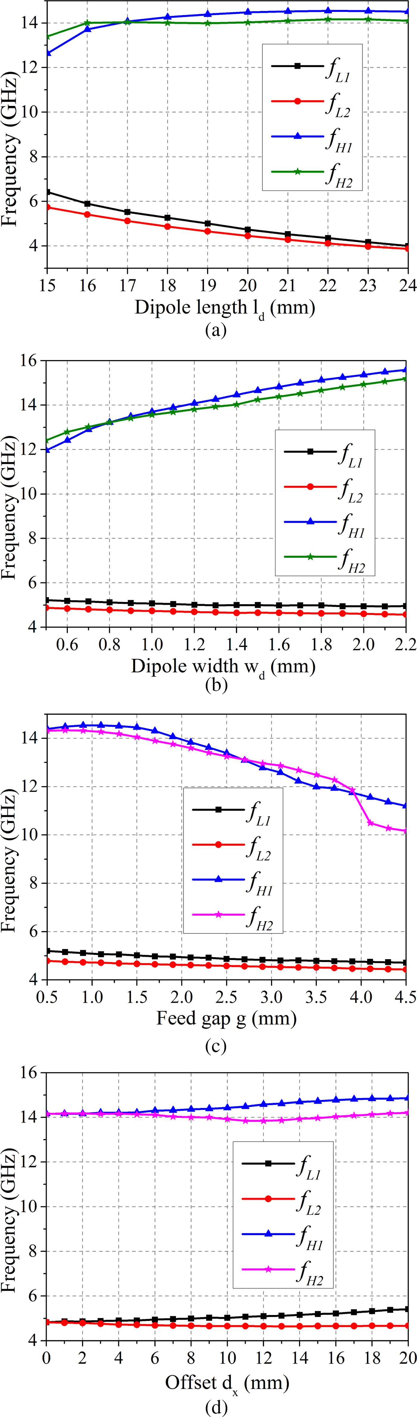
Fig. 3. Lower and upper band edge frequency variation with respect to various design parameters, (a) Dipole length, (b) Dipole width, (c) Dipole feed gap and (d) Offset d x.
Ultra-wideband performance of the proposed array is achieved by utilizing high inter-element coupling. There are two types of mutual interactions present in the proposed array. First, the coupling due to near-field radiation of the antenna elements and second the capacitive coupling between the edges of the dipole of the same row.
To verify this, the effect of variation in the inter-element spacing d y and dipole edge gap s are analyzed for an infinite array. These two parameters control the inter-element coupling in the proposed array. Active reflection coefficient at port 1 for different values of s is shown in Fig. 4(a). For the smaller value of s, the bandwidth of the array is large but active reflection coefficient at the mid frequencies is nearly touching − 10 dB. Therefore, the value of s is to be chosen properly to achieve wider bandwidth with a good input impedance match over the entire band. Effect of inter-element spacing d y on the performance of the proposed array is shown in Fig. 4(b). As d y increases, the mutual coupling between the dipoles decreases which reduces the impedance bandwidth of the proposed array. Same can be observed from the parametric results that by increasing d y, the lower and upper band edge frequencies are approaching towards each other which results in the reduction in the impedance bandwidth.
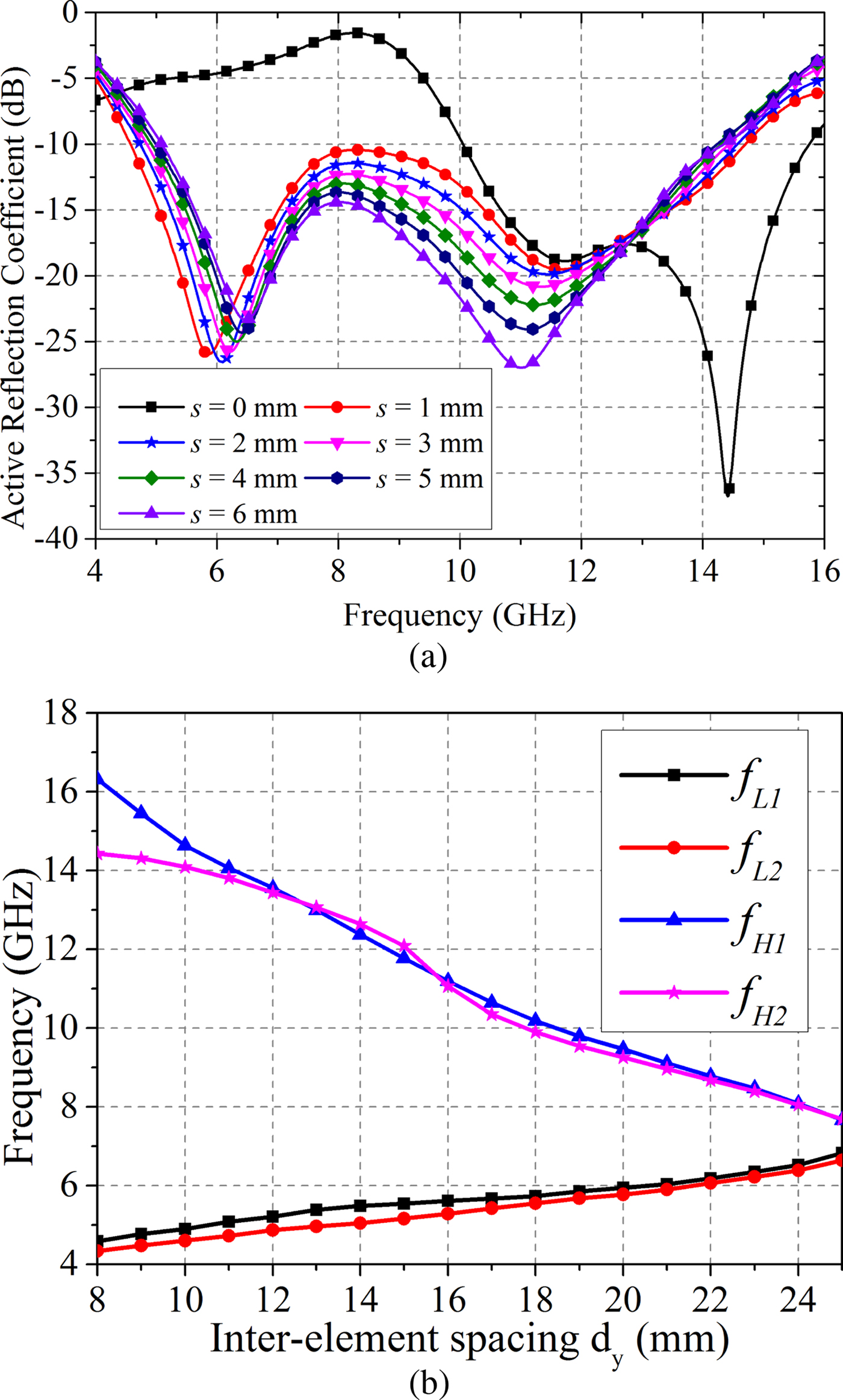
Fig. 4. Effect of inter-element coupling on the performance of the proposed array, (a) variation of dipole edge gap s and (b) variation in inter-element spacing d y.
Finite array analysis
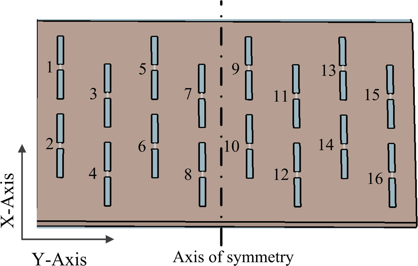
The layout of 2 × 8 elements finite array with the element numbers is shown in Fig. 5. Various properties of the proposed finite array without feed network are analyzed in this section.

Fig. 5. The layout of 2 × 8 finite array.
The proposed array has certain symmetries and hence, various results of the finite array are discussed only for half the number of elements (element 1 to element 8). Active reflection coefficients for different elements of finite array are shown in Fig. 6(a). Due to the small size of the array, the active reflection coefficient of array elements is different for inner and edge elements. Instead of making the performance of every element identical, it is easier to make the operating band of each element same. Variation of the active reflection coefficient with frequency could be different for each of the elements. To observe coupling between the elements of the finite array, the elements are excited individually and complete scattering matrix of the array is obtained. The reflection coefficient of the element 8 and its coupling with the rest of the elements are shown in Fig. 6(b). It is observed from the results that the impedance bandwidth of the element without taking mutual coupling into account isa narrow band in nature. Mutual coupling for the inner element (say element 8) is high for the closer elements and it is gradually decreasing as the distance between the elements is increasing.
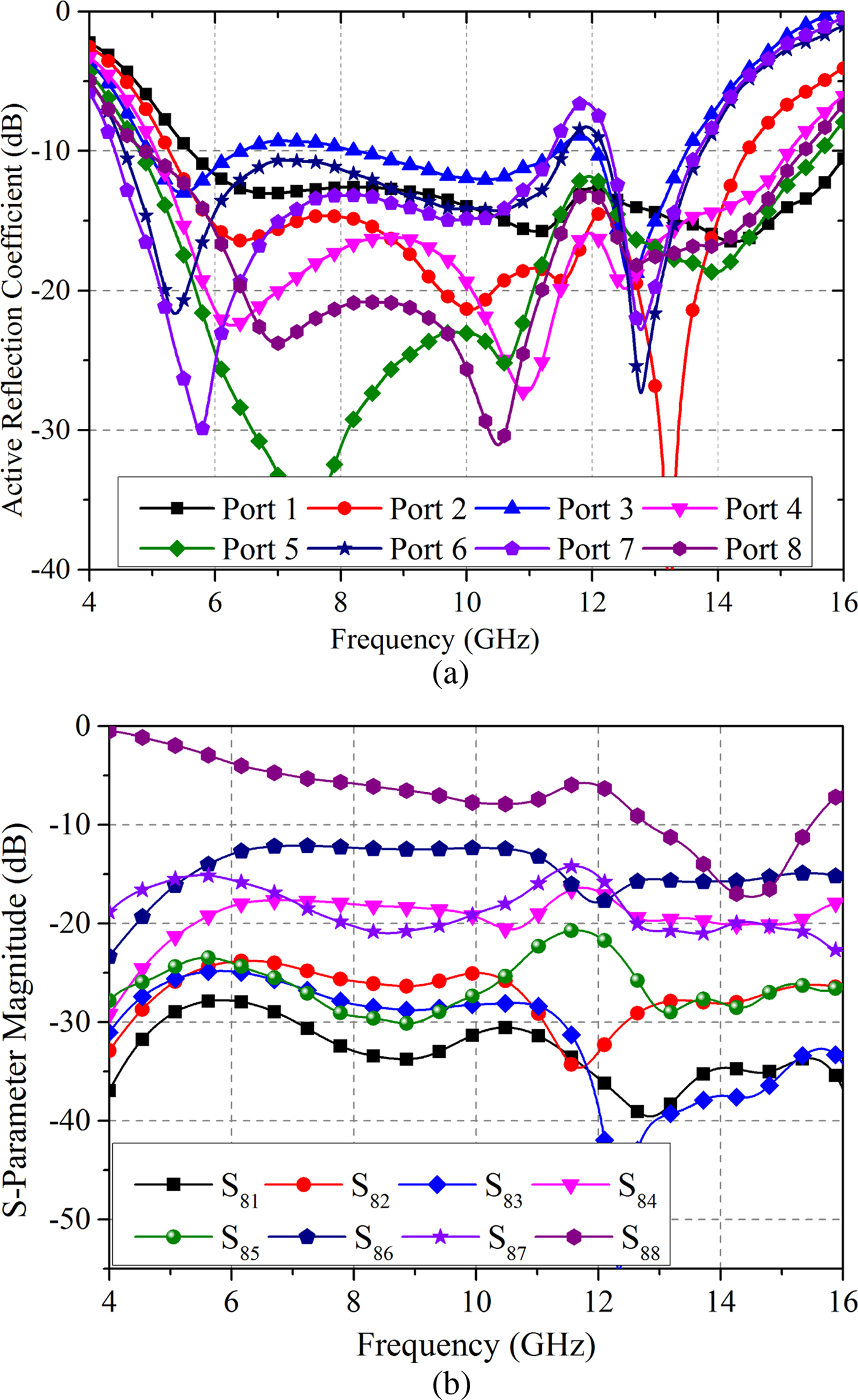
Fig. 6. Reflection coefficient of the proposed array (a) active reflection coefficient of the finite antenna array (all elements are excited) and (b) reflection coefficient of element 8 and its coupling to other element (only 8th element is excited rest of the elements are terminated in matched load).
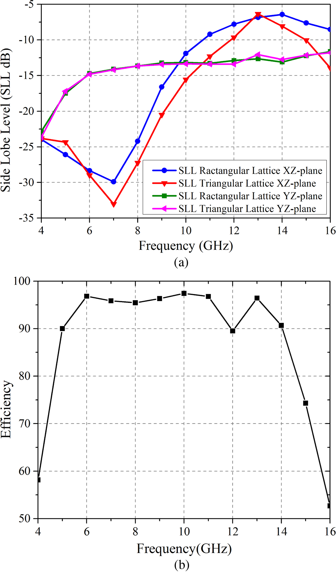
To demonstrate the advantage of using a triangular lattice, the radiation properties of a rectangular lattice array are compared with the proposed triangular lattice array. Rectangular lattice array is just created by setting offset d x = 0 and rest of the dimensions are the same in both the arrays. Side lobe level for the proposed and rectangular lattice arrays in both XZ and Y Z planes are shown in Fig. 7(a). In the XZ-plane, side lobe level is improved for the triangular lattice compared with rectangular lattice. In the Y Z-plane, there is no effect on the side lobe level by varying the lattice from rectangular to triangular. To solve the high side lobe problem without affecting the impedance bandwidth of the array, use of the triangular lattice is a good option. The total efficiency of the finite array, as shown in Fig. 7(b), is better than 90% over the band of interest. The realized gain and the aperture efficiency of the proposed antenna array is shown in Fig. 8. The realized gain of the array is nearly constant over the frequency band of the interest. At low-frequency operations, the aperture efficiency is high. It decreases with the frequency. Over the band of interest, more than 50% aperture efficiency is obtained.

Fig. 7. Side lobe level and efficiency of the finite array (a) Comparison of side lobe level of proposed triangular lattice with rectangular lattice and (b) Total efficiency.
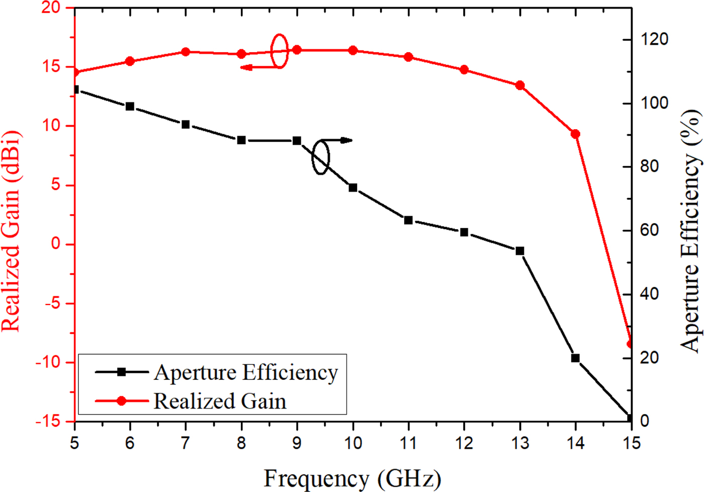
Fig. 8. Realized gain and aperture efficiency of the proposed antenna array.
Feed network design
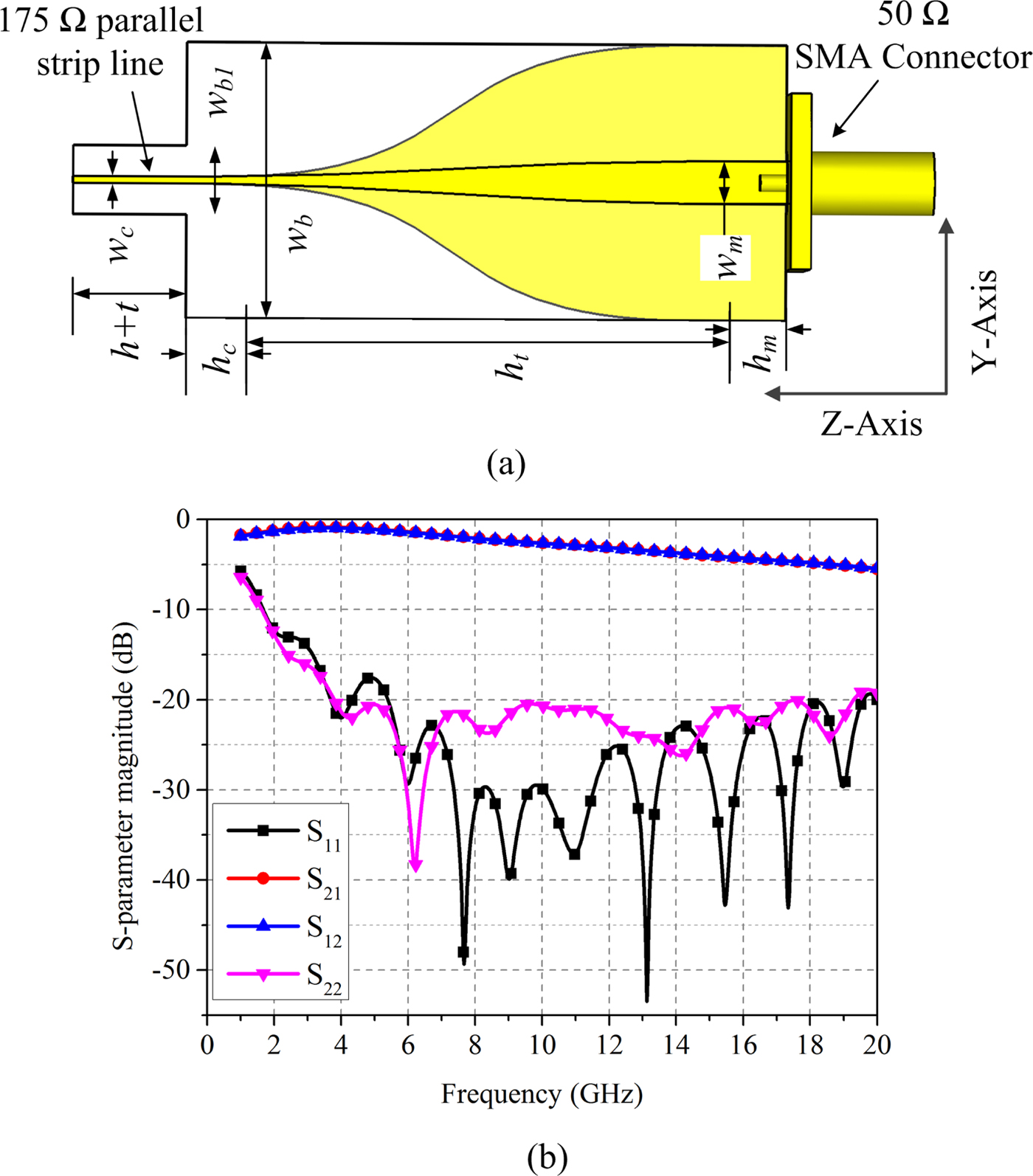
In the previous sections, discrete ports of 175 Ω are used to analyze the finite array. To physically test the array, we need to excite the array using 50 Ω coaxial lines. For this, an ultra-wideband feed network is required. In this section, an ultra-wide band feed network along with proposed 2 × 8 finite array is studied. The feed network consists of 16 individual feeds. For each element, a parallel strip to microstrip line UWB balun is designed to provide 175 Ω to 50 Ω impedance transformation. Thegeometry of the feed network element is illustrated in Fig. 9(a). To implement the balun, FR-4 (εr = 4.4) substrate is used. Wave port excitation for each port is chosen in the simulation of the balun. The magnitude of the S-parameters of the balun is shown in Fig. 9(b). It can be observed from the results that the performance of the balun is good over 2–20 GHz frequency band. Due to the lossy nature of FR-4 substrate, high insertion loss at the higher frequencies is observed. Various dimensions of the balun are given in the caption of Fig. 9.

Fig. 9. Feed network element, (a) Geometry of parallel strip to microstrip balun and (b) magnitude of S-parameters of balun. Various dimensions of balun are as follows: w c = 0.5, w m = 3.1, w b = 20, w b1 = 5, h c = 2, h m = 7, h t = 36, h = 6, t = 1.6. All dimensions are in mm.
The feed network is arranged in such a way that its presence will havea minimum effect on the performance of the array. To achieve this, a section of parallel strip line on a narrow substrate is extended over the balun. The wider section of the substrate is placed below the reflector of the antenna array. However, the narrow section passes through the reflector and the dipole substrate and is connected to the dipoles. From Fig. 5, it can be observed that there are four dipoles in one column. Although the array is 2 × 8 in nature, due to the triangular lattice, these dipoles are arranged in four columns. Four baluns are printed on a single substrate to feed four dipoles ofa single column. The position of the baluns for the adjacent columns is shifted by distance d y. Assembly of the feed network is shown in Fig. 10(a). Spacers are used to maintain the proper distance between the balun substrates. The metallic reflector is placed over the feed network and the extended parallel strip lines pass through the holes of diameter w b1 in the reflector. Complete assembly of the array is shown in Fig. 10(b). Plexiglas spacers of height h are used at the edges ofa substrate on which dipoles are printed to provide uniform support and spacing between the substrate and the reflector. Rectangular openings of length g 1 and width w b1 are created in the dipole substrate for the extended parallel strip line. The major effect of the feed network on the performance of the antenna array is due to the holes in the metallic reflector made for the extended parallel strip line. Back lobe is observed in the radiation pattern of the array due to these holes. A metallic shield, as shownin Fig. 10(b), is used to suppress the back lobe. Final dimensions of the array are optimized with the complete feed network and given in the caption of Fig. 10.
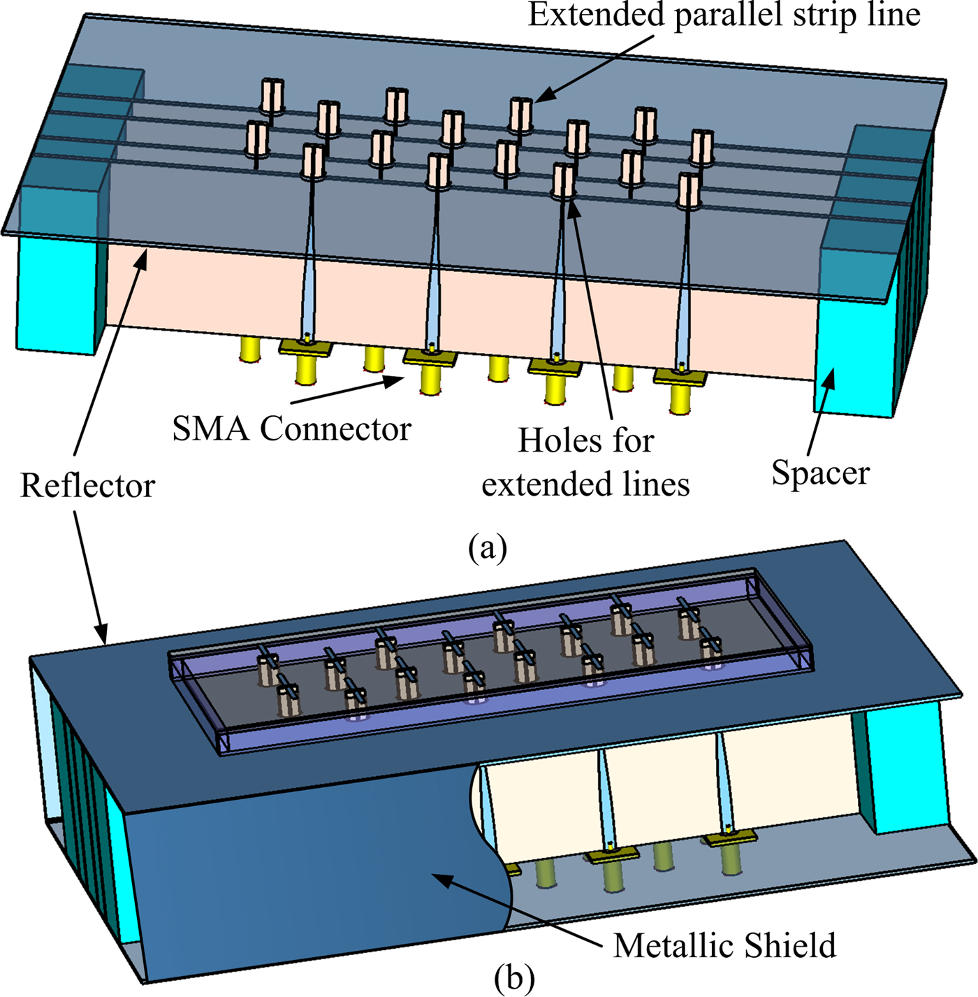
Fig. 10. Different building blocks of proposed array, (a) complete feed network with SMA connectors and (b) complete assembled proposed array. Final optimized dimension of the array with feed network is as follows. g = 1.6, d y = 16, d x = 12, l d = 23, w d = 1.5, h = 6, s = 5, and t = 1.6. All dimensions are in mm.
Results and discussion
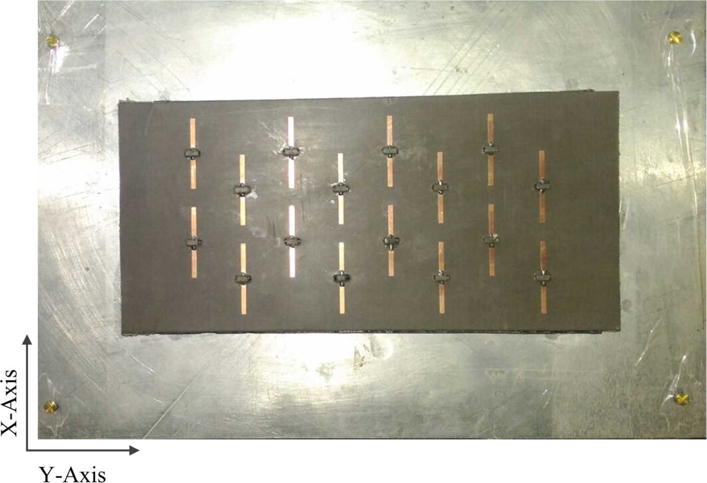
To validate the proposed antenna array as discussed in the previous sections, a 2 × 8 elements finite array is fabricated and tested. A fabricated prototype of the proposed array is shown in Fig. 11. To compute the active reflection coefficient of the fabricated antenna array, reflection coefficient of all elements and their coupling with all other elements are measured. This is carried out by connecting two ports of the antenna array to the network analyzer while the rest of the elements are terminated with the matched load. Measurement for all the combination is done to complete the 16 × 16 scattering matrix of the fabricated 16 port antenna array. Further, the active reflection coefficient is computed from the measured scattering matrix by the use of equation (1) [Reference Kalfa and Halavut20].
 $$\{S_i \}_{active}=[S] \{V_i \}_{excitation},$$
where {V i}excitation is the excitation coefficient vector and [S] is measured scattering matrix.

Fig. 11. Fabricated prototype of proposed array.
In this case, uniform excitation without any phase shift is used to compute the active reflection coefficient. To compute active reflection coefficient for any particular scan angle, appropriate progressive phase shift can be introduced in the excitation coefficient vector. Measured and simulated active reflection coefficients of the antenna array are plotted in Fig. 12. A good match between the measured and simulated active reflection coefficient of the proposed array is obtained. To obtain the radiation pattern of the fabricated antenna array, active element pattern [Reference Pozar21] of each element is measured by connecting the transmitter to one of the elements and terminating all other elements ina matched load. The vector sum of all active element patterns is used to compute the measured radiation pattern of the proposed antenna array. Fig. 13 shows the measured and simulated radiation pattern of the proposed antenna array in XZ-plane and Y Z-plane. Broadside gain of the proposed antenna array for 5 and 8 GHz are 14.7 and 16.4 dBi, respectively. There is good agreement between measured and simulated pattern along the main beam. There are some discrepancies in the side lobe measurement results. Error in measurement could be due to the dimensional errors which occur because of the manufacturing tolerance. This affects the measured phase which in turn hasa significant influence on the side lobe performance of the array. The second issue is with the measurement setup of the fabricated array. To do vector sum of active element patterns, both magnitude and the phase are needed to be measured. Even small errors in phase measurement badly affect the side lobe performance of the fabricated antenna array. Measured and simulated radiation pattern of the proposed antenna array for different scan angles are shown in Fig. 14. The patterns for 30° and 45° scan angle are plotted for 5 and 7 GHz. A significant good match is observed between the measured and simulated results. The gain of the patterns shown in Fig. 14(a), Fig. 14(b), Fig. 14(c), and Fig. 14(d) are 14, 13.9, 15.5, and 14.5 dBi, respectively.
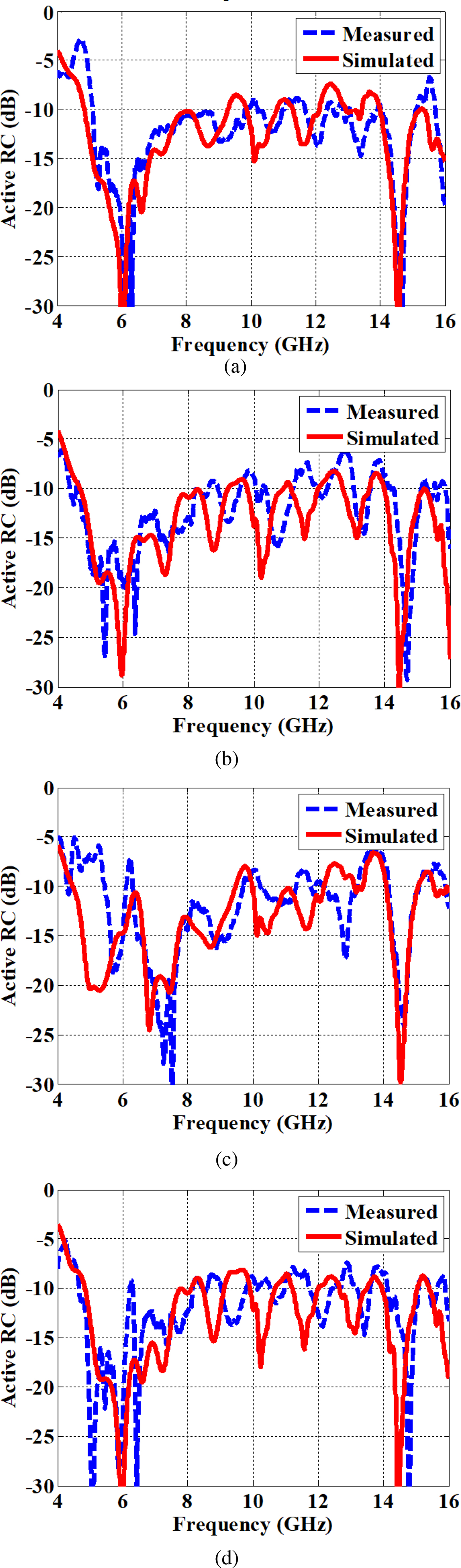
Fig. 12. Measured and simulated active reflection coefficient of the proposed array, (a) port 1, (b) port 3, (c) port 5, and (d) port 7.
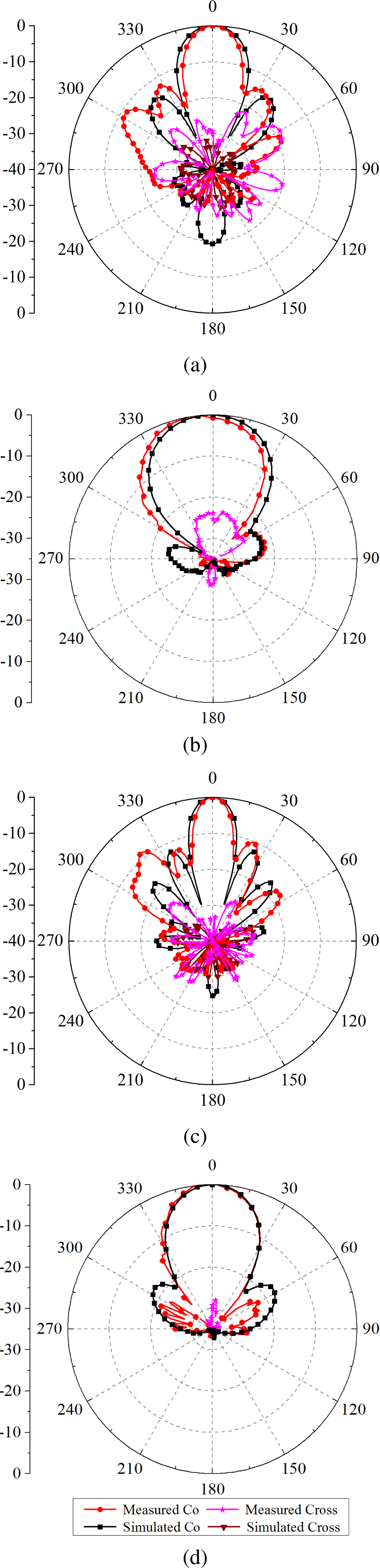
Fig. 13. Measured and simulated radiation pattern of the proposed array in XZ and Y Z plane, (a) 5 GHz Y Z-plane, (b) 5 GHz XZ-plane, (c) 8 GHz Y Z-plane, and (d) 8 GHz XZ-plane.
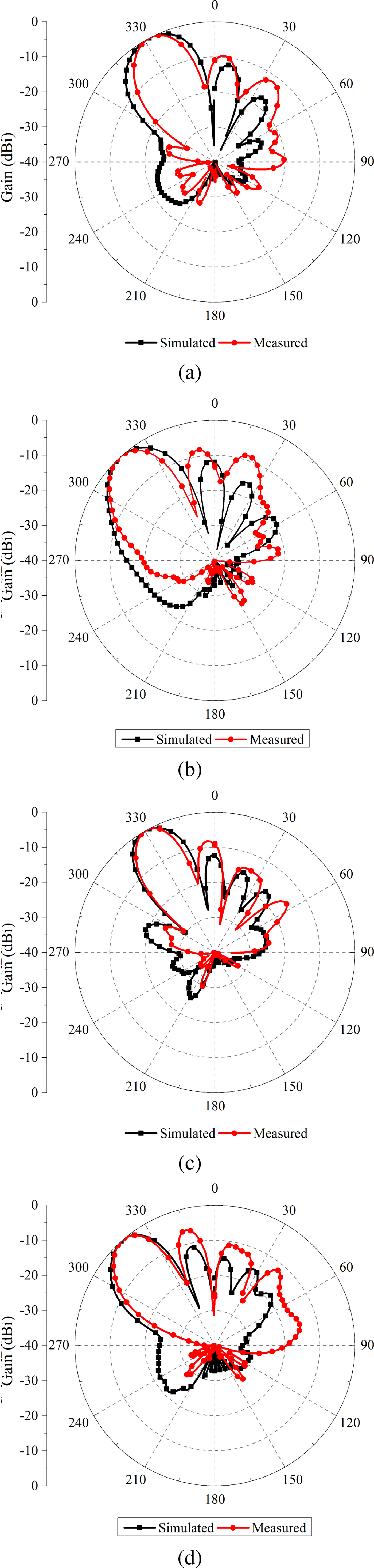
Fig. 14. Measured and simulated beam scanning pattern of the proposed array, (a) 5 GHz − 30° scan, (b) 5 GHz − 45° scan, (c) 7 GHz − 30° scan, and (d) 7 GHz − 45° scan.
Conclusion
A compact wideband 2 × 8 elements tightly-coupled antenna array is presented. By the utilization of the triangular lattice 3–4 db reduction in the side lobe level of the XZ-plane pattern is observed. The efficiency is more than 90% over the band of operation of the antenna array. From the proposed array 2.8:1 impedance bandwidth is obtained. Excellent radiation characteristics are observed over the entire frequency band of interest. A good match between measured and simulated results is observed.
Author ORCIDs
Abhishek Kumar Awasthi 0000-0003-4880-9733
 Abhishek K. Awasthi did B.Tech. in electronics and communication from Uttar Pradesh Technical University (UPTU), Lucknow in 2008. He received his M.Tech. degree in digital communication from GGSIP University, Delhi in 2011. He received his doctoral degree from the Department of Electrical Engineering of Indian Institute of Technology Kanpur. He is currently an assistant professor with the Department of Electronics and Communication Engineering, Amity University Jharkhand Ranchi. His current research interests include antenna array analysis and microwave measurement.
 A. R. Harish received the Ph.D. in Electrical Engineering from the Indian Institute of Technology Kanpur, Kanpur, India. He was with Com Dev Wireless, Dunstable, UK, and was a visiting faculty at the University of Kansas. He is currently a professor with the Department of Electrical Engineering, Indian Institute of Technology Kanpur. His current research interests include antenna analysis, microwave measurements, microwave circuits, radio-frequency identification, and computational electromagnetics.