


Introduction
With the ever increasing demand worldwide for high-speed data transmissions among mobile terminals, the components involved in the wireless communication links such as antennas, amplifiers, power dividers, transmission lines, and transitions have been under intensive study during the past decades [Reference Yang, Gao, Luo, Wen, Ban, Yang, Ren and Wu1–Reference Dong, Johansen, Zhurbenko and Hanberg15]. In order to achieve larger bandwidths within a limited spectrum, these components are pushed to operate at higher frequencies which already reach the ranges of millimeter-wave and terahertz (THz) frequencies. For example, the existing fifth generation mobile network occupies Ka-band from 26.5 to 40 GHz [Reference Rappaport, MacCartney, Samimi and Sun16–Reference Lu, You, Wang, You, Huang and Wu19], whereas the upcoming sixth generation mobile network will operate at frequencies above 100 GHz [Reference Rappaport, Xing, Kanhere, Ju, Madanayake, Mandal, Alkhateeb and Trichopoulos20–Reference Boulogeorgos, Alexiou, Merkle, Schubert, Elschner, Katsiotis, Stavrianos, Kritharidis, Chartsias, Kokkoniemi, Juntti, Lehtomaki, Teixeira and Rodrigues22]. Under this circumstance, the challenging requirements of designing antennas for high-speed data transmissions at such high frequencies are wideband operation with a relatively high gain and being versatile for circuit integrations.
Split-ring resonator is usually associated with metamaterials, which are synthesized by including resonant metallic shapes within a host dielectric [Reference Wang, Dong and Itoh23–Reference Pendry, Holden, Robbins and Stewart27]. Compared with conventional wideband planar antennas such as dipole and slot antennas, split-ring resonators can provide a higher gain, while the occupation area is within the same level as the conventional patch antennas. Though most of the split-ring resonators reported in the literature are designed for narrow band operation at specific frequencies [Reference Hu, Wang, Yan and Ai28–Reference Bait-Suwailam, Boybay and Ramahi33], some studies still show the potential of designing wideband split-ring resonators for high-speed data transmissions. According to [Reference Dong, Johansen, Zhurbenko and Hanberg15], the designed split-ring resonator based on a rectangular ring structure achieves a fractional bandwidth of 36% centered at 140 GHz and it is implemented as a wideband transition between rectangular waveguide and coplanar waveguide (CPW). In [Reference Kakhki, Dadgarpour, Antoniades, Sebak and Denidni34], the split-ring resonators are placed on top of a dipole antenna for gain enhancement at Ka band, while the bandwidth of the dipole antenna is maintained.
In the recent years, low-cost and high-performance components used for wireless communication systems at millimeter-wave and THz frequencies are blooming, especially for the components based on substrate integrated waveguide (SIW) [Reference Parment, Ghiotto, Vuong, Duchamp and Wu35]. As an alternative to conventional air-filled rectangular waveguide, SIW is light-weighted, compact, and versatile for system integrations at the expenses of slightly increased dielectric loss and degraded power-handling capability. The dimensions can be downscaled by a factor of $\sqrt {\epsilon _r}$ , in which εr represents the relative permittivity of the dielectric substrate. Compared with conventional planar transmission lines such as microstrip and CPW, SIW has a self-shielded structure which makes it an ideal candidate for the applications requiring low transmission loss and large bandwidths. Besides, for communication systems, the electric fields inside a SIW can be split or combined easily. Thus, it becomes attractive especially for the components operating at millimeter-wave frequencies [Reference Taringou, Bornemann and Wu36]. Compared with conventional air-filled rectangular waveguides with predefined dimensions and standardized flanges, SIWs are normally customized for different applications and dielectric substrates. In addition, integrated circuits at millimeter-wave frequencies still rely on planar structures due to their fabrication processes. As a result, transitions from planar transmission lines as well as rectangular waveguides to SIWs are necessary and have been extensively investigated [Reference Mohamed and Sebak37–Reference Patrovsky, Daigle and Wu44]. When designing transitions, not only the characteristic impedances but also the propagation modes need to be matched so that it can provide a large bandwidth and a low transmission loss at the same time [Reference Mao, Hwang, Ruey-Beei and Chen45].
When SIW is used as the transmission line, as one of the advantages, the power splitting process is simplified so that the electric fields are easily distributed to each element in the antenna array. Different types of antenna arrays based on SIW for Ka-band applications can be found in the literature. In [Reference Yang, Yu, Dong, Zhou and Hong5], an SIW is inserted into a tapered horn structure forming the so-called tapered slot antenna. The proposed 1×4 antenna array can provide 9 dBi of gain at 30 GHz. However, the power distribution network is not involved and the antenna array needs to be fed by four individual paths. As is reported in [Reference Mak, So, Lai and Luk18], a leaky-wave antenna together with 18 magnetoelectric dipoles aligning in a line achieves a gain of 15 dBi at 30 GHz. For feeding the antenna array, coaxial-to-rectangular waveguide and rectangular waveguide-to-SIW transitions are also included in the design. According to [Reference Ren, Hong and Wu46], an SIW is inserted perpendicular into a patch from the backside of the substrate forming a three-dimensional (3D) microstrip antenna. By implementing an orthogonal SIW power divider, the proposed 2×2 antenna array exhibits a gain of 10 dBi at 30 GHz. Other designs based on SIWs exhibit promising results by using slot antennas [Reference Liu, Yang, Jin and Zhu47–Reference Liu, Hong, Kuai, Yin, Luo, Chen, Tang and Wu50], patch antennas [Reference Xu, Zhou, Zhou, Wu, Yu and Hong51–Reference Li, Wang and Dou53], and lens antennas [Reference Malik, Doychinov, Zaidi, Robertson and Somjit54–Reference Jaschke, Rohrdantz, Mitto and Jacob56].
The purpose of this paper is to introduce a wideband split-ring resonator and the corresponding antenna arrays based on SIW for Ka-band applications. The components are designed and verified using full-wave electromagnetic simulations in Ansys Electronics Desktop (EDT, formerly known as HFSS) while the prototypes are fabricated and tested. As the fundamental transmission lines involved in the designs, CPW and SIW based on Rogers 6002 substrate are presented at the beginning. After that, wideband CPW-to-SIW and coaxial-to-CPW transitions are explained in detail. A transition prototype including 2.92 mm coaxial connectors (K-connectors) is designed, fabricated, and tested in a back-to-back configuration. The concept of designing a two-stage SIW power divider is described so that the power can be equally distributed to each element in an antenna array. A wideband split-ring resonator operating at Ka band is designed and the possible arrangements for implementing antenna arrays are introduced afterwards. As a demonstrator proving the concepts, a 2×2 antenna array prototype is developed in a compact format by combing the designed components. The full layout, electric field distribution, and assembly structure of the antenna array prototype are illustrated. The fabrication process and experimental setups in particular the method for characterizing radiation patterns are explained. The simulation and measurement results are compared at the end.
Transmission lines and wideband transitions
CPW and SIW
For a conventional CPW patterned on the top of a dielectric substrate, the signal trace is aligned in the middle of two separated ground traces. In this case, the electric fields mainly exist in the gaps between the signal and ground traces. However, for a more common and realistic situation, when a bottom ground plane is added under the dielectric substrate it forms the so-called conductor-backed coplanar waveguide (CB-CPW). In particular, for thin dielectric substrates, part of the electric fields is coupled to the bottom ground plane, which might result in unexpected mixed-mode propagations, radiations, and resonances. The CPW shown in Fig. 1 is based on a Rogers 6002 substrate with a thickness of 508 μm. It is designed to achieve a characteristic impedance of 50 Ω at Ka band. The dielectric constant (εr) and dissipation factor (tanδ) of the substrate are 2.94 and 0.0012, respectively. The CPW is patterned on the top layer, whereas the bottom layer works as the ground plane. The material of the conductor layers is copper and it has a thickness of 35 μm. By implementing vias along the CPW, the electric fields are restricted in a specific region on the substrate. Thus, the parasitic modes are suppressed and the bandwidth is enlarged. Instead of hollow plated vias, silver epoxy is used for filling the holes on the substrate.

Fig. 1. CPW based on Rogers 6002 substrate.
As illustrated in Fig. 2, an SIW is designed using the same dielectric substrate. The vias going through the substrate work as the vertical conductor walls which form a dielectric-filled waveguide structure on the substrate. The distance between the vias is kept as small as possible in order to prevent the electric fields leaking from the gaps. As the fundamental transmission lines, the CPW and SIW are involved in designing the transitions, power divider, and split-ring resonator.

Fig. 2. SIW based on Rogers 6002 substrate.
CPW-to-SIW transition
In order to feed the antenna array by a coaxial connector, CPW is chosen to be the intermediate transmission line between the coaxial and SIW. In this case, as a complete design, both transitions are designed and optimized for providing a wideband matching at Ka band. When connecting a CPW to a SIW, one of the possible approaches is to terminate the slots so that the signal and ground traces of the CPW are merged into the top conductor wall of the SIW. For achieving a large bandwidth, the propagation mode must convert from CPW to SIW modes smoothly at the transition. Besides, the parasitic modes and radiations caused by the mode conversion should be taken into account and suppressed. Otherwise, extra losses might be introduced. The designed CPW-to-SIW transition is demonstrated in detail in Fig. 3.

Fig. 3. CPW-to-SIW transition.
At the beginning, the slots are extended 1.5 mm and turned 40° away from the signal trace on both sides. Before the termination, the slots are turned back to their original direction and the width is reduced gradually from 300 to ~ 50 μm within a distance of 0.6 mm. The vias have a diameter of 1 mm and their positions are optimized by moving towards to the slots as close as possible. However, for a realistic design, the minimum center-to-center distance between the adjacent vias is kept more than 1.2 mm while a distance of 0.2 mm is reserved between the edges of the vias and the slots. In this way, the electric fields become more concentrated in the dielectric substrate from the signal trace to the vias as well as the bottom ground plane. It promotes the migration of electric fields from the slots on the top to the dielectric substrate so that an SIW propagation mode is generated at the end of the transition.
Coaxial-to-CPW transition
As shown in Fig. 1, for the designed CPW, the widths of the signal trace and the gap are 1.2 and 0.3 mm, respectively, whereas it does not fit the coaxial feed. In addition, the attached K-connector needs to be fixed to the bottom metal carrier by screws. Thus, two through holes with a diameter of 1.5 mm are reserved on the dielectric substrate. The positions of the through holes are determined by the K-connector while it turns out to be overlapped with the vias along the CPW. That means the vias in the overlapped area need to be rearranged and its performance should also be investigated. In order to compensate the dimensional differences and convert to a CPW propagation mode smoothly, as illustrated in Fig. 4, a coaxial-to-CPW transition is implemented.

Fig. 4. Coaxial-to-CPW transition.
For aligning the K-connector, a tapered structure is implemented at the beginning of the transition. The widths of the signal trace and the gap are reduced to 0.8 and 0.2 mm, respectively. By taking into account the length of the pin, the CPW prior to the tapered structure is extended 0.5 mm. The vias on the first row are placed alongside the tapered structure and they locate 0.7 mm away from the edge of the dielectric substrate. Besides, the distance between the vias on the first and second rows is increased to 2.6 mm so that there is enough space for realizing the through holes. Once the screws are mounted, the through holes on the substrate are filled with metal conductor and can be treated as large vias.
Prototype, fabrication, and experimental results
The designed transition prototype in a back-to-back configuration is shown in Fig. 5. The overall length and width of the dielectric substrate are 29.4 and 10 mm, respectively. In the simulations, by using wave ports, the electric fields are excited at the input and output. The reflections caused by the structural discontinuities between the K-connectors and the dielectric substrate are also taken into account. Furthermore, an aluminum carrier, four steel screws, and an air cavity with radiation boundary conditions on the top of the dielectric substrate are included in the simulation.

Fig. 5. Transition prototype in a back-to-back configuration.
Fig. 6 illustrates the magnitude of electric field distributions on the top surface of the designed transition prototype at 28 and 40 GHz, respectively. A coaxial mode is excited at the input of the K-connector and propagates to the dielectric substrate where a CPW mode is generated at the end of the coaxial-to-CPW transition. After that, the electric fields are guided along the CPW and concentrate not only in the gaps between the signal and ground traces but also in the dielectric substrate between the signal trace and the bottom ground plane. At the CPW-to-SIW transition, the propagation mode converts to an SIW mode when two slots on the top surface move away from each other and terminate gradually. At both frequencies, the vias behave as expected and no visible leakage, parasitic mode, or radiation can be observed from the electric field distributions. However, with increasing frequency, the electric fields tend to leak into the dielectric substrate especially from the gaps between the vias on the first and second rows.

Fig. 6. Electric field distributions of the designed transition prototype at 28 and 40 GHz.
In order to prove the concept, the designed transition prototype in a back-to-back configuration was fabricated in-house. The Rogers 6002 substrate with top and bottom copper layers was ordered from a commercial supplier. The layout was repeated and patterned on the substrate by using a low-cost printed circuit board (PCB) technology, which requires a minimum gap or the conductor width of 200 μm for a stable prototyping. During the patterning process, the positions of the vias as well as through holes were also marked on the top surface. After that, the substrate was inspected under a microscope for imperfections and diced into pieces. The holes were drilled on the dielectric substrate by using a spinner with a radius of 500 μm. Four of them serve as through holes for screws while the others were filled with silver epoxy (PELCO, Ted Pella). The dielectric substrate was cleaned by acetone afterwards for removing the overflowed silver epoxy as well as unexpected dusts on the surfaces.
Fig. 7 demonstrates the assembly structure and the fabricated transition prototype. The K-connectors (HK-LR-SR2, Hirose Electric) were fixed to the aluminum carrier by two steel screws going through the dielectric substrate from the bottom. In this case, the through holes have to be drilled accurately so that the pin of the K-connector could be aligned right to the middle of the CPW. Once the K-connector is tightly fixed, soldering is unnecessary and the pin is attached to the conductor layer by mechanical force.

Fig. 7. Assembly structure and fabrication of the designed transition prototype in a back-to-back configuration.
A vector network analyzer (Anritsu ME7808B) was used to measure the scattering parameters of the fabricated transition prototype. Besides, the effects of the cables and adapters were calibrated out before each measurement. The measurement results of the designed transition prototype in a back-to-back configuration are shown in Fig. 8 by the solid lines. In comparison, the dashed lines represent the simulation results. From 26 to 40 GHz, the measured return loss remains better than 11.2 dB and the measured insertion loss is <2.5 dB. When the bandwidth refers to the frequency band where the return loss is better than 10 dB, the fabricated transition prototype exhibits a bandwidth of at least 14 GHz. At the same time, each fabricated transition contributes <1.25 dB insertion loss at Ka band. Compared with the simulation results, a reasonable agreement is achieved, while the differences are mainly caused by the simulation modeling process and fabrication tolerance. In particular, the K-connector was only simulated partially. According to the data sheet provided by the supplier, when two K-connectors were tested by using a straight transmission line with a length of 25 mm, the measured insertion loss is around 2.5 dB at 40 GHz. Furthermore, the εr and tanδ variations of the dielectric substrate due to different operating frequencies were not included in the simulation.

Fig. 8. Simulation and measurement results of the designed transition prototype in a back-to-back configuration.
Power divider design consideration
Single-stage SIW power divider
As an advantage of using SIW, the electric fields can be easily split and distributed to each element in an antenna array. Fig. 9 shows the designed single-stage SIW power divider in detail. The input of the power divider is connected to the output of the CPW-to-SIW transition as shown in Fig. 3. The electric fields propagate inside the SIW and reach the via in the middle of the power divider which work as a conductor post splitting the electric fields equally into two ways. The positions of the vias as well as conductor post are optimized so that the designed SIW power divider exhibits a wideband matching at Ka band.

Fig. 9. Single-stage SIW power divider.
Two-stage SIW power divider
Since the power needs to be equally distributed to four split-ring resonators, three identical SIW power dividers are cascaded by connecting the outputs of the first stage SIW power divider to the inputs of the second stage SIW power dividers. As shown in Fig. 10, the designed two-stage SIW power divider has one input and four outputs. In the simulations, wave ports are used as the excitation scheme and an SIW mode is excited at the input. The magnitude of electric field distribution at 30 GHz inside the designed two-stage SIW power divider is also illustrated in Fig. 10. The electric fields are excited at the input and propagate along the SIW until it hits the conductor post. During the power splitting process, the electric fields are divided into two ways and later four ways. As a result, four outputs have the same amplitude and phase.

Fig. 10. Layout of the two-stage SIW power divider and its electric field distribution at 30 GHz.
Fig. 11 shows the simulated scattering parameters of the designed two-stage SIW power divider. The return loss is better than 10 dB from 27 to 37 GHz with an associated insertion loss of 7 dB. It corresponds to a fractional bandwidth of 31.3% centered at 32 GHz. Thus, as a wideband SIW power divider, it is used for designing the antenna arrays.

Fig. 11. Simulation results of the two-stage SIW power divider.
SIW antenna arrays
Split-ring resonator
As shown in Fig. 12, the split-ring resonator is designed as a single element operating at Ka band. It is realized by etching two circular slots on the top conductor wall of the SIW. The annular ring is developed and connects to a circular patch in the middle. The distance between the vias is kept as small as possible for preventing wave leakage. At the same time, their positions are optimized for maximizing the bandwidth at Ka band. Compared with a conventional rectangular patch antenna, the occupation area and gain of the split-ring resonator are within the same level while it provides a larger bandwidth. In addition, the split-ring resonator is versatile for integrating with other components and compatible with different types of transmission lines such as microstrip, CPW, and SIW. When the split-ring resonator is integrated with an SIW, it can provide a moderate power-handling capability which is an advantage in particular for communication systems at millimeter-wave frequencies. Fig. 12 also illustrates the magnitude of electric field distribution of the designed split-ring resonator at 30 GHz. The electric fields are guided to the split-ring resonator by a SIW and radiated into free space. On the top surface of the dielectric substrate, strong radiations can be observed at the annular ring, circular patch, and slots. Due to the vias around the split-ring resonator, the electric fields are restricted mainly inside the SIW and resonator so that the wave leakage from the edges remains at a low level.

Fig. 12. Layout of the split-ring resonator and its electric field distribution at 30 GHz.
Fig. 13 shows the simulated radiation pattern of the designed split-ring resonator at 30 GHz. The half-power beamwidths are 56° and 106° on the xz-plane (φ = 0°) and yz-plane (φ = 90°), respectively. In the simulations, a wave port is used as the excitation scheme and an SIW mode is excited at the input of the split-ring resonator. For simulating radiation characteristics, a large air cavity with radiation boundary conditions is added around the split-ring resonator reaching the antenna far-field region.

Fig. 13. Radiation pattern (directivity) of the split-ring resonator at 30 GHz.
The simulated return loss and gain of the designed split-ring resonator are shown in Fig. 14. The return loss remains better than 10 dB from 27.5 to 33.5 GHz, which corresponds to a fractional bandwidth of 19.7% centered at 30.5 GHz. In the direction perpendicular to the split-ring resonator (φ = 0°, θ = 0°), a maximum gain of 7.7 dBi is realized at 31.5 GHz. Besides, the gain variation is still <3 dB from 28.8 to 33.6 GHz. As a single element, the designed split-ring resonator achieves not only a large bandwidth but also a sufficient gain and in-band gain uniformity, which makes it suitable for wireless communication systems at Ka band.

Fig. 14. Return loss and gain of the split-ring resonator.
Antenna array consideration
When being implemented into an antenna array, the designed split-ring resonator, SIW power divider, coaxial-to-CPW, and CPW-to-SIW transitions are combined into a full layout. In this case, as a complete design, the developed antenna array can be connected directly to the existing components or communication systems through a coaxial connector. In general, depending on the applications, antenna arrays are optimized for a higher gain or a specific radiation pattern by adjusting the amplitude and phase of the electric fields, arrangement and distance between the adjacent elements. Figure 15 demonstrates four possible arrangements for implementing antenna arrays with four split-ring resonators. Figure 15(a) illustrates the arrangement of a basic 1×4 antenna array, where the split-ring resonators locate next to each other aligning in a line. Four inputs have the same amplitude and phase. In comparison, a 1×4 antenna array with offset split-ring resonators is shown in Fig. 15(b). The distance between the adjacent elements is further reduced while the amplitude and phase of the inputs are kept unchanged. When the antenna array is arranged in a 2×2 format, as shown in Fig. 15(c), the split-ring resonators are symmetrically aligned. In order to have the main lobe towards the direction perpendicular to the antenna array, four inputs are divided into two groups with the same amplitude and a phase difference of 180°. Another possible arrangement is illustrated in Fig. 15(d). The split-ring resonators are aligned in a cross format. Although four inputs have the same amplitude, a phase difference of 90° is applied to the adjacent elements.

Fig. 15. Possible arrangements of four split-ring resonators. (a) 1×4 antenna array (line), (b) 1×4 antenna array (offset), (c) 2×2 antenna array (symmetry), (d) 2×2 antenna array (cross).
The radiation patterns of the corresponding antenna arrays with four split-ring resonators at 30 GHz are simulated and shown in Fig. 16. In the simulations, wave ports are used as the excitation scheme and an air cavity with radiation boundary conditions is added around the dielectric substrate. Four inputs have the same amplitude, while the phase is adjusted according to each arrangement so that the maximum radiation can be achieved in the direction perpendicular to the antenna array. The simulated maximum directivities for the possible arrangements and the corresponding half-power beamwidths at 30 GHz are listed in Table 1. Furthermore, the return losses and in-band directivities of the corresponding antenna arrays with four split-ring resonators are also investigated and shown in Fig. 17. Due to the vias going through the dielectric substrate, the elements in the antenna arrays are almost independent from each other so that the return loss of the single element is not affected and a large bandwidth can be achieved when being implemented into antenna arrays. As for the directivity, the maximum values mainly depend on the arrangement of split-ring resonators. In comparison with the single element, similar variations and in-band uniformity can be observed.

Fig. 16. Simulated radiation patterns (directivity) of the antenna arrays with four split-ring resonators at 30 GHz.

Fig. 17. Simulated return losses and directivities (φ = 0°, θ = 0°) of the antenna arrays with four split-ring resonators.
Table 1. Simulated maximum directivities (D 0) and half-power beamwidths (HPBWs) of the antenna arrays with four split-ring resonators at 30 GHz.

As shown in Fig. 18, when combining the designed components and routing paths, two full layouts of the antenna arrays with four split-ring resonators are addressed by following the arrangements illustrated in Figs 15(a) and 15(c), respectively. In order to realiz, the corresponding arrangements, SIW extensions and turning structures are implemented at the outputs of each SIW power divider. The electric fields are fed to the dielectric substrate though a coaxial input and equally distributed to each split-ring resonator. For the layout shown in Fig. 18(a), four routing paths of the antenna array are designed to be identical so that the electric fields at the split-ring resonators could have the same amplitude and phase. The overall length and width of the layout are 90 and 70 mm, respectively. In another case, for the layout shown in Fig. 18(b), four routing paths of the antenna array are divided into two groups having different path lengths. The two routing paths on the right of the dielectric substrate are designed to be 2.9 mm longer than the others. Thus, a phase difference of 180° could be achieved at 30 GHz among the split-ring resonators. Due to the increased complexity and physical length of the routing paths, the layout occupies a larger area which leads to a length of 75 mm and a width of 120 mm. In general, when an antenna array consists of a large number of elements, the routing paths might become complicated and require advanced integration methods. Furthermore, Figs 18(c) and 18(d) illustrate the magnitude of electric field distributions at 30 GHz. While being fed by a K-connector, the propagation mode is converted to an SIW mode at the beginning. Due to the power dividers and the losses caused by the routing paths, the magnitude reduces to less than a quarter when the electric fields reach the split-ring resonators.

Fig. 18. Designed SIW antenna arrays with four split-ring resonators: (a) full layout of the 1×4 antenna array (line) with routing paths, (b) full layout of the 2×2 antenna array (symmetry) with routing paths, (c) electric field distribution of the 1×4 antenna array (line) with routing paths at 30 GHz, and (d) electric field distribution of the 2×2 antenna array (symmetry) with routing paths at 30 GHz.
Antenna array prototype and fabrication
For proving the concepts and validating the designs, an antenna array prototype is developed by combing the coaxial-to-CPW transition, CPW-to-SIW transition, two-stage SIW power divider, and split-ring resonators. Fig. 19 shows the full layout of the designed 2×2 antenna array prototype in a compact format, where the split-ring resonators are directly connected to the outputs of the two-stage SIW power divider. In this case, compared with the SIW antenna arrays shown in Fig. 18, the overall length and width of the layout are reduced to 63 and 45 mm, respectively. However, as a tradeoff, the distances between the adjacent split-ring resonators (d x and d y) are more than a half wavelength at 30 GHz. Since the designed antenna arrays can be easily rearranged and optimized for a specific application, the prototype is merely used as a demonstrator at the expense of having grating lobes in the radiation pattern. In the simulations, for accuracy improvement, the K-connector is also included and a coaxial mode is excited at the input using a wave port. The magnitude of electric field distribution of the designed 2×2 antenna array prototype at 30 GHz is also illustrated in Fig. 19. The electric fields are guided through the transitions at the beginning and the propagation mode converts to an SIW mode. After that, the electric fields are equally distributed to each split-ring resonator and radiated into free space. In addition, a weak wave leakage can be observed on the dielectric substrate due to the gaps between the adjacent vias especially on the edges of the split-ring resonators.

Fig. 19. Full layout of the designed 2×2 antenna array prototype and its electric field distribution at 30 GHz.
The fabricated 2×2 antenna array prototype and its assembly structure are shown in Fig. 20. The chosen dielectric substrate and coaxial connector have been previously verified at Ka band by the fabricated transition prototype. The layout was firstly patterned on a Rogers 6002 substrate using a low-cost PCB process. After that, the holes were drilled on the dielectric substrate and filled with silver epoxy. For not affecting the radiation pattern of the antenna array, six Teflon screws were used for fixing the dielectric substrate to the bottom aluminum carrier. The K-connector was attached to the dielectric substrate at the last step. Two steel screws were used and fixed from the backside of the aluminum carrier. The pin of the K-connector was aligned to the middle of the CPW. When being inspected under a microscope, imperfections were observed at the edges of the slots between the signal and ground traces.
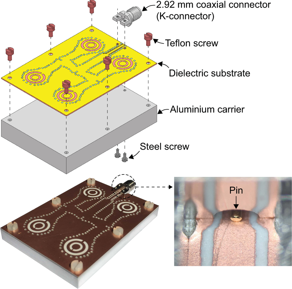
Fig. 20. Assembly structure and fabricated 2×2 antenna array prototype.
Experimental results
At the beginning, the return loss of the fabricated 2×2 antenna array prototype was measured at Ka band using a vector network analyzer (Anritsu ME7808B). The effects of the cables and adapters were calibrated out prior to the measurement. The solid line in Fig. 21 represents the measured return loss of the fabricated 2×2 antenna array prototype. In comparison, the simulation result is shown by the dashed line and a good agreement is achieved. The measured return loss remains better than 10 dB from 27 to 34 GHz, which corresponds to a fractional bandwidth of 23.0% centered at 30.5 GHz. In addition, the fabricated 2×2 antenna array prototype exhibits another possibility of operating from 36 to 37.4 GHz.

Fig. 21. Simulated and measured return losses of the designed 2×2 antenna array prototype.
For the next step, the radiation patterns of the fabricated 2×2 antenna array prototype were measured in the DTU-ESA Spherical Near-Field Antenna Test Facility by employing the spherical near-field antenna measurement technique. Being intended for the determination of antenna characteristics in the range from 500 MHz to 40 GHz, the test facility is operated in cooperation between the Technical University of Denmark (DTU) and the European Space Agency (ESA). According to the method introduced in [Reference Hansen57], the antenna under test (AUT) needs to be mounted on a tower that can rotate along two axes (θ-axis and φ-axis). Besides, a probe is implemented at a finite distance away so that the AUT can be scanned at specific points on a sphere with a predetermined radius. As a part of the measurement procedure, the calibration is carried out in the test facility before measuring the AUT in which the radiation characteristics of the probe are acquired. After that, the radiation pattern of the AUT can be derived by solely using the sample points measured during the spherical scan. Therefore, it becomes possible to achieve the far-field behavior of the AUT by measuring its near-field characteristics in a closed and controlled environment. Fig. 22 demonstrates the DTU-ESA Spherical Near-Field Antenna Test Facility for measuring the radiation pattern of the fabricated 2×2 antenna array prototype.
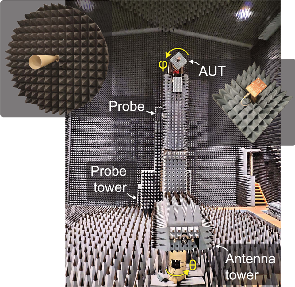
Fig. 22. DTU-ESA Spherical Near-Field Antenna Test Facility for measuring the radiation pattern (directivity) of the fabricated 2×2 antenna array prototype.
During the spherical measurement process, the co-polarization and cross-polarization directivity components were achieved separately while the total directivity of the fabricated 2×2 antenna array prototype was calculated accordingly. The solid lines in Fig. 23 illustrate the measured directivities at 30 GHz on the xz-plane (φ = 0°) and yz-plane (φ = 90°), respectively. In comparison, the dashed lines represent the simulated directivities. The measurement results coincide with the simulation results. However, minor differences can be observed in the radiation patterns since the frame for mounting the AUT on the antenna tower and the coaxial cable connecting to the AUT were not included in the simulation. The fabricated 2×2 antenna array prototype achieves a measured maximum directivity of 15.0 dBi at 30 GHz when φ = 0° and θ = 8°. The measured co-polarization and cross-polarization directivity components at 30 GHz on the xz-plane (φ = 0°) and yz-plane (φ = 90°), respectively, are shown in Fig. 24 as a supplement. In addition, the simulated and measured grating lobe levels in the radiation patterns are listed in Table 2.

Fig. 23. Simulated and measured radiation patterns (directivity) of the designed 2×2 antenna array prototype at 30 GHz.

Fig. 24. Measured co-polarization and cross-polarization directivity components of the designed 2×2 antenna array prototype at 30 GHz.
Table 2. Simulated and measured grating lobe levels of the designed 2×2 antenna array prototype at 30 GHz.

a P n refers to the nth lobe in the radiation pattern when θ ranges from 0° to 180°.
b T n refers to the nth lobe in the radiation pattern when θ ranges from 0° to − 180°.
As a demonstrator, the 2×2 antenna array prototype successfully proves the concepts, the simulation methods, the designed components including the transitions, SIW power divider, and split-ring resonator. However, since the variations of εr and tanδ were not taken into account in the simulations, a 1.2 dBi difference can be observed for the maximum directicity at 30 GHz. For a specific application, the components can be easily rearranged to a different format. When the antenna array is integrated on a PCB board, FR4 is normally used as the dielectric substrate. In this case, it should also be possible to optimize the designs while keep their performances. In Table 3, this work is compared with other SIW antenna arrays published in the literature for Ka-band applications. The designed 2×2 antenna array is noticeable when taking into account the bandwidth and directivity at the same time. In addition, it provides a compact and complete solution with a K-connector feed which can be directly applied to the existing wireless communication systems at Ka band.
Table 3. Comparison between this work and published SIW antenna arrays at Ka band.

a The value refers to the maximum gain or directivity that is achieved at the specified frequency.
b The bandwidth refers to the width of the frequency band where the return loss is better than 10 dB.
c RW is the abbreviation of rectangular waveguide.
Conclusion
In this work, wideband split-ring antenna arrays based on SIW for Ka-band applications have been presented. The concepts of designing CPW, SIW, coaxial-to-CPW transition, and CPW-to-SIW transition were explained and the effect of adding silver epoxy-filled vias was discussed. The CPW and SIW were designed based on a thin Rogers 6002 substrate and simulated using Ansys Electronics Desktop. The designed coaxial-to-CPW and CPW-to-SIW transitions were described in detail and a transition prototype was fabricated in a back-to-back configuration. The measured returns loss is better than 11.2 dB from 26 to 40 GHz and each fabricated transition contributes <1.25 dB insertion loss. In order to distribute the power equally to four split-ring resonators, a two-stage SIW power divider was implemented. The simulated return loss is better than 10 dB from 27 to 37 GHz. The split-ring resonator was designed and its dimensions were illustrated. As a single element, the designed split-ring resonator achieves a simulated fractional bandwidth of 19.7% centered at 30.5 GHz. It can also provide a simulated gain of 7.7 dBi at 31.5 GHz and a sufficient in-band gain uniformity at the same time. In addition, four possible arrangements of the split-ring resonators were introduced and their radiation patterns were compared. Two full layouts of the antenna arrays were addressed by combining the designed components and routing paths. As a demonstrator, a 2×2 antenna array prototype in a compact format was developed. The antenna array prototype was fabricated using a low-cost PCB technology. The return loss was measured using a VNA and the radiation pattern was characterized in the DTU-ESA Spherical Near-Field Antenna Test Facility. The fabricated antenna array achieves a measured directivity of 15.0 dBi at 30 GHz with a fractional bandwidth of 23.0% centered at 30.5 GHz. Therefore, it proves the concepts while the designed antenna array can be rearranged to a different format for a specific application at Ka band.
Acknowledgments
The authors thank M. Nielsen, J. Lauridsen, and J. N. Mortensen at the Department of Electrical Engineering, Technical University of Denmark for assisting the fabrication processes.
 Yunfeng Dong received the B.Sc. degree in Electronic Information Engineering from the Beijing University of Technology (BJUT), Beijing, China, in 2012, the M.Sc. and Ph.D. degrees in Electrical Engineering from the Technical University of Denmark (DTU), Kongens Lyngby, Denmark, in 2014 and 2019, respectively. From 2011 to 2012, he was an exchange student with the South-Eastern Finland University of Applied Sciences (XAMK), Mikkeli, Finland. In 2014, he was a research assistant with the Electromagnetic Systems Group (EMS), DTU, where he holds a post-doctoral position. In 2017, he was a visiting scholar with the Terahertz Devices and Systems Group, Technische Universität (TU) Darmstadt, Darmstadt, Germany. His research interests include developing innovative strategies that are suitable for hybrid integration and packaging at millimeter-wave and terahertz frequencies, on-chip antennas, and antenna arrays for high-speed wireless communications, characterizing conductivity, and shielding effectiveness.
 Vitaliy Zhurbenko received the M.Sc. degree in Electrical Engineering from the Kharkiv National University of Radio Electronics, Kharkiv, Ukraine, in 2001, and the Ph.D. degree in Electrical Engineering from the Technical University of Denmark (DTU), Kongens Lyngby, Denmark, in 2008. In 2005, he joined DTU, where he is currently an associate professor. His current research and teaching interests include microwave and millimeter-wave sensing for biomedical and security applications, microwave, and millimeter-wave components and integrated circuits for instrumentation applications, antennas and passive circuit design and characterization, and magnetic resonance technology.
 Kyriakos Kaslis received his B.Sc. degree in Computer Engineering and Informatics from the University of Patras, Patras, Greece, in 2015 and the M.Sc. degree in Electrical Engineering from the Technical University of Denmark (DTU), Kongens Lyngby, Denmark, in 2017. From September 2017 to December 2017, he was a research assistant with the Electromagnetic Systems Group (EMS), DTU, where he is currently a project engineer. His research interests include spherical near-field measurements, microwave measurements, and antenna theory.
 Jeppe Majlund Bjørstorp was born in Esbjerg, Denmark in 1976. He received the M.Sc. degree in engineering from the Technical University of Denmark (DTU), Kongens Lyngby, Denmark, in 2002. In 2002, he joined the Electromagnetic Systems Group (EMS), DTU, as a research assistant, where he is currently operating the DTU-ESA Facility. His main areas of research include uncertainty analysis in spherical nearfield antenna measurements and antenna gain determination.
 Tom Keinicke Johansen received the M.Sc. and Ph.D. degrees in Electrical Engineering from the Technical University of Denmark (DTU), Kongens Lyngby, Denmark, in 1999 and 2003, respectively. In 1999, he joined the Electromagnetic Systems Group (EMS), DTU, where he is currently an associate professor. From September 2001 to March 2002, he was a visiting scholar with the Center for Wireless Communication, University of San Diego, San Diego, CA, USA. He has spent several external research stays at the Ferdinand Braun Institute (FBH), Berlin, Germany. His research interests include the modeling of high-frequency solid-state devices, millimeter-wave, and submillimeter-wave integrated circuit design.


