I. INTRODUCTION
Substrate integrated waveguide (SIW) is a promising candidate for microwave and millimetre-wave application. It is composed of two rows of metallic vias or slots in a dielectric substrate that connect two parallel metallic plates. In this way, the non-planar rectangular waveguide (RWG) can be fabricated in planar form with a normal printed circuit board (PCB) process or low-temperature co-fired ceramic (LTCC) technology. SIW structures can be equivalent to classical RWGs filled with dielectric. Therefore, SIW structures inherit most of the advantages of conventional RWGs, such as high-Q, high power capability, and relatively low-loss. Furthermore, compactness, low-profile, low-cost, and easy integration are also realized in SIWs when compared to RWGs. In recent years, a vast range of SIW active elements and passive components, such as filters, antennas, couplers, power dividers, and oscillators, have been proposed and studied.
The SIW components need to be interconnected with an external system frequently, such as network analyzers. Therefore, an effective transition is required and the commonly used interconnection is the SIW-to-microstrip transition or SIW-to-CPW transition. However, as frequency increases to millimetre-waves, serious losses especially high conductor losses prevent the application of this type of transition. Consequently, various types of SIW-to-RWG transitions are required.
Basically, there are two main geometrical configurations of SIW-to-RWG transitions as summarized in [Reference Głogowski, Zürcher, Peixeiro and Mosig1]: an in-line configuration where the main axes of both waveguides are collinear and a right-angle where the two axes are perpendicular. The in-line transitions have been studied to obtain wide bandwidth using probes inserting into waveguide taper [Reference Xia, Xu, Yan, Li, Guo and Wang2–Reference Li, Meng and Dou7]. For right-angle transitions, the energy is commonly coupled through an aperture etched on the broad wall of SIW [Reference Głogowski, Zürcher, Peixeiro and Mosig1, Reference Kai, Hirokawa and Ando8–Reference Li, Chen, Khazaka and Wu12]. The main mode of both waveguides is TE10 mode and the propagation of electromagnetic field is only allowed when the coupling aperture is resonant. Therefore, the bandwidth of the right-angle transitions is still limited. A transition utilizing a piece of dielectric substrate with two gaps inserted into a RWG for matching to SIW has been studied [Reference Kai, Hirokawa and Ando8], and 3.6% bandwidth with the reflection smaller than −15 dB is measured. A stepped SIW structure has been introduced [Reference Kai, Hirokawa and Ando9], and it shows stable performance against the mechanical tolerance compared to conventional transition. The measured bandwidth with reflection below −15 dB is about 11.4% but it is only applicable to SIWs using thick substrate. Transitions between LTCC substrate and RWG have been presented in [Reference Huang and Wu10, Reference Huang and Wu11] and resonating cavities are employed to obtain wide bandwidth. Less than 9% bandwidths with −15 and −13 dB return loss are achieved separately. In [Reference Li, Chen, Khazaka and Wu12] the substrate of SIW can be easily surface-mounted to the standard flange of the RWG and a longitudinal slot window etched on the broad wall of SIW has been designed for coupling energy between SIW and RWG. This structure has a very simple configuration and it has been widely used in SIW components feeding, but the bandwidth is limited due to the resonant property of the slot window. The measured bandwidth with a return loss less than −10 dB is only 3.14%. A modification has been done in [Reference Głogowski, Zürcher, Peixeiro and Mosig1] and two resonances are obtained using a pair of slots with different lengths. It provides a broader bandwidth and the measured bandwidth (at 15 dB return loss) is 1.72 GHz which corresponds to a 6.6% of fractional bandwidth.
In this paper, a novel wideband right-angle transition structure composed of a multi-section SIW with a rectangular aperture etched on the broad wall and two stepped ridges embedded in the RWG flange is proposed. It provides a wide bandwidth over the K/Ka-band. Two back-to-back transitions in different lengths are designed and fabricated. The experimental results have good agreement with the simulations.
II. CONFIGURATION DESIGN
The cut-off frequency of SIW (represented by fc) is designed in accordance with WR-28 standard waveguide (with width W f = 7.112 mm and height H f = 3.556 mm), which is 21.08 GHz. The SIW is made out of a 0.254 mm-thick Rogers RT/Duroid 5880 substrate with tanδ = 0.0009 and ε r = 2.20. The ground plane is formed by a 17 µm-thick layer of copper, covering the whole substrate. The equivalent width of SIW a eff can be obtained from
 $$a_{eff} = \displaystyle{c \over {2f_c \sqrt {\varepsilon _r } }}.$$
Furthermore, the width of SIW a SIW can be calculated from the following equation [Reference Kordiboroujeni and Bornemann13]:
 $$a_{SIW} = a_{eff} + p\lpar 0.766e^{0.4482d/p} - 1.176e^{ - 1.214d/p} \rpar \comma \;$$
where, p is the distance between adjacent metallic vias, and d represents the diameter of metallic vias. The applicable range of equation (2) covers all practical SIW applications in condition of 0.5 < d/p < 0.8 [Reference Deslandes and Wu14]. The dimensions of the input SIW are: p = 0.72 mm, d = 0.5 mm, and d/p = 0.694. Therefore, numerical values are: a eff = 4.8 mm and a SIW = 5.2 mm.
The configuration of proposed transition is illustrated in Fig. 1. This structure is inspired by an E-plane bend waveguide structure which could own a wide bandwidth by properly designed. The SIW is end up with a multi-section structure widening to the RWG width and it also can be seen as a tapered SIW section. A rectangular aperture etched on the broad wall is located at the center of the last section. It can be seen that the substrate is too thin comparing with RWG and the transmission mode in both waveguides is interrupted by the coupling aperture which cause a limited bandwidth. As we all know, the ridge in RWG can be used to concentrate the electric field and it is suitable for transiting from a conventional RWG to a reduced height RWG. Furthermore, the ridge can be designed as steps to reduce the return loss. Thus, the stepped ridges with different dimensions are introduced to obtain a broadband impedance matching and they are embedded in RWG flange for convenience. The number of ridges should be more than one in order to obtain the excellent performance. However, it is difficult to fabricate the ridged RWG flange when the number of ridges exceeds three. Therefore, only two stepped ridges are adopted and they can be easily fabricated on the RWG flange by numerical control machine (the mechanical tolerance is within ±0.02 mm). The flange is sandwiched between SIW and RWG when doing measurements. Thus, the energy coming from WR-28 standard waveguide is concentrated on the top of ridge, and then coupled into SIW through the rectangular aperture. The parameters L r1 and L r2 represent the length of ridge 1 and ridge 2, respectively. The other details and associate variables of the transition are depicted in Fig. 2. To take account of the physical composition of interface, the width (W s) and length (L s) of the end SIW section should be larger than the dimensions of RWG.

Fig. 1. Configuration of the proposed transition.
Fig. 2. Top view of the proposed transition.
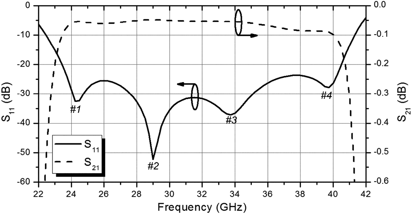
The tapered SIW section, adjustable rectangular coupling aperture, and stepped ridges are introduced to achieve a wide bandwidth and in fact the proposed transition can be seen as a multi-section matching transformer. However, the number of parameters will also increase which leads to a difficult design. Therefore, the genetic algorithm is used here to optimize these parameters and the simulations are carried out using the full-wave simulator High Frequency Structure Simulator (HFSS). The optimal values are summarized in Table 1. The simulated results of a single transition working at center frequency 31.5 GHz are depicted in Fig. 3. The dielectric loss and metal loss are also considered. It can be observed that ‘four resonant frequency points’ are obtained and the bandwidth with return loss better than 20 dB is about 17 GHz which corresponds to a 53.9% of fractional bandwidth. The insertion loss is less than 0.1 dB over this bandwidth.
Fig. 3. Simulated results of a single transition.
Table 1. Design parameters and optimized values.

In order to further investigate the characteristics of this structure and find the optimal solution, a parameter study was carried out. The key parameters of the proposed transition are analyzed by changing one parameter at a time and fixing the others as shown in Table 1. Figures 4(a), 4(b), and 4(c) show the effects of ridge 1 on return loss of the proposed single transition. It can be seen that with the parameter L r1 increasing, the first resonant point shifts to the lower frequency band at the cost of deteriorating return loss. The middle two resonant points become to one by decreasing the parameter W r1. The return loss is sensitive to the height of ridge 1 (H r1) and the best result is obtained at H r1 = 2.20 mm. The effects of ridge 2 are shown in Figs 5(a), 5(b), and 5(c). It is observed that the return loss between the first two resonant points become better with the parameter L r2 increasing but become worse between the last two resonant points. Furthermore, the middle two resonant points shifts to lower frequency band. The parameter W r2 only has a little effect on the higher frequency band. The parameter H r2 has the similar effect to the parameter W r1 and the best impedance matching is achieved at H r2 = 0.59 mm.
Fig. 4. Simulated return loss for various parameters of ridge 1; (a) L r1, (b) W r1, and (c) H r1
Fig. 5. Simulated return loss for various parameters of ridge 2; (a) L r2, (b) W r2, and (c) H r2
Figures 6(a) and 6(b) show the effects of the rectangular coupling aperture. It can be seen that the return loss becomes better around the first resonant point with the increase of aperture length (L c), but considering the whole frequency band the best impedance matching is achieved at L c = 2.08 mm. For the lower value of parameter W c, the return loss around the last two resonant point becomes worse but the higher value may cancel the last resonant point. Therefore, W c = 4.45 mm is suitable. The effects of the tapered SIW section are depicted in Figs 7(a) and 7(b). The return loss become better at the lower frequency band but become worse around the last three resonant points with the increase of tapered section length L t. The parameter W t has the opposite effect on impedance matching. The best performance is achieved at L t = 2.76 mm and W t = 6.79 mm, respectively.
Fig. 6. Simulated return loss for various parameters of coupling aperture; (a) L c and (b) W c.
Fig. 7. Simulated return loss for various parameters of tapered SIW section; (a) L t and (b) W t.
In a word, by weighing the effect of every parameter and choosing the appropriate value, a wide bandwidth impedance matching is feasible. The propagations of the electromagnetic waves in the transition at the resonant frequencies are shown in Fig. 8. It can be seen that with the increase of frequency, a ‘higher mode’ is excited within the transition that can be seen in Fig. 8(d) and the ‘four resonant frequencies’ may be generated due to the interference of the waves between the discontinues in the transition.
Fig. 8. The propagations of electromagnetic waves in the transition at the resonant frequencies (a) 24.25 GHz, (b) 29 GHz, (c) 33.75 GHz, and 39.75 GHz.
III. SIMULATION AND EXPERIMENTAL RESULTS
The transitions were cascaded back-to-back for measurement and two samples with different lengths were fabricated, as depicted in Fig. 9. The losses of SIW can be estimated in order to ensure the measured performance of transition accurately. The measurements were taken using an Agilent 8363E network analyzer. The simulated and measured results of shorter sample are shown in Fig. 10. The measured bandwidth is about 12.15 GHz (corresponds to a 38.57% bandwidth) with a return loss better than 14.5 dB and insertion loss less than 1.45 dB. The attenuation of the SIW is evaluated to be 0.0278 dB/mm by comparing the transmission coefficients of the two prototypes. The length of the shorter SIW sample is 21 mm and the introduced loss is about 0.58 dB. Therefore, the insertion loss of a single transition is less than 0.44 dB. As far as we know, it is the widest bandwidth right-angle transition between SIW and RWG.
Fig. 9. Photography of the proposed back-to-back transitions.
Fig. 10. Simulated and measured results of the proposed back-to-back transitions.
Due to the mechanical tolerance is within ±0.02 mm and the simulated results shown in Figs 4–7 show that this mechanical tolerance has little effect on the impedance matching. The difference between simulated and measured results around 38 GHz is mainly caused by the dislocation of flange along y-axis and the change of copper thickness (copper_t). In spite of adopting pins, there is still a mounting error f y (the mounting error of flange along y-axis) between flange and SIW. Figure 11 gives simulated result about the dislocation which shows as f y increasing, the return loss around 38 GHz becomes worse. In addition, the copper covered on the substrate is thickened when the vias of SIW are metallized. Figure 12 depicts return loss for various copper_t. It is observed that with the increase of copper_t the return loss becomes worse over the whole working band. Therefore, the existed mounting error and fabricating error caused the difference between simulated and measured results. The performance of transition can be well improved by reducing these errors.
Fig. 11. Simulated return loss of a single transition with different f y.
Fig. 12. Simulated return loss of a single transition with different copper_t.
Table 2 depicts the comparison between the proposed right-angle transition and the reported structures. Due to these transitions are interfaced with the standard RWGs, the cross-sections are in the same with the standard RWG flanges and only the thickness of the transitions (including the thickness of substrate) are shown for comparison. The added thickness in this work is caused by the RWG flange which can be conveniently sandwiched between SIW and RWG. It can be observed that this novel structure improves the performance very well and can be widely used for microwave and millimeter-wave communication, radar and measuring systems.
Table 2. Comparison between this work and some reported works.

IV. CONCLUSION
A novel wideband right-angle transition between thin SIW and RWG based on multi-section structure is proposed. A rectangular aperture etched in the end of the multi-section SIW and two stepped ridges embedded in the RWG flange are used to obtain a wideband impedance matching. Measured results agree well with simulations. Experimental results show a return loss better than 14.5 dB over 12.15 GHz which correspond to a 38.57% bandwidth. The insertion loss for a single transition is below 0.44 dB. Due to simple structure, compact size, low loss, and wide bandwidth, this right-angle transition can be widely used for microwave and millimetre-wave communication, radar, and measuring systems.
ACKNOWLEDGEMENT
We are particularly grateful to the editor and reviewers for their valuable comments and suggestions. This work was supported by the Advance Research Foundation under grant 9140A01010114JW06.
Teng Li received his B.S. degree in Xiamen University, Xiamen, China, 2009. He is currently pursuing his Ph.D. degree at State Key Laboratory of Millimeter Waves, Southeast University, Nanjing, China. His current research includes millimeter wave antenna and passive circuit.
Wenbin Dou graduated from the University of Science and Technology of China, Hefei, in 1978. He received his Master and Ph.D. degrees from the University of Electronic Science and Technology of China in 1983 and 1987, respectively, both in Electronics and Communications. From 1987 to 1989, he worked in Southeast University as a postdoctoral fellow. Since 1989, he has been with the State Key Laboratory of Millimeter Waves, Southeast University. In 1994, he was promoted to professor. He is vice director of the State Key Laboratory of Millimeter Waves. His research interesting include ferrite devices, millimeter wave quasi-optics, millimeter wave focal imaging, antennas and scattering, millimeter wave binary optics, and so on.