I. INTRODUCTION
In recent years, the demand for higher data rates, higher quality of service and more flexible interface for wireless communication systems has increased drastically. Multi-input multi-output (MIMO) system is one of the most promising techniques that can be utilized to meet those requirements. A MIMO system uses multiple antennas at the transceivers to improve the capacity and enhance the reliability [Reference Biglieri1]. The efficiency of a MIMO system is dependent on the physical antenna design. Among the techniques for MIMO antenna design, compact printed antennas have attracted much attention thanks to their advantageous features such as low-profile, low-cost, and ease of fabrication and integration. Several types of printed antennas have been proposed for MIMO applications. This includes a triple-band E-shaped printed monopole antenna [Reference AliNezhad and Hassani2], monopole antennas using neutralization-line technique for WiFi dongle [Reference Su, Lee and Chang3], and planar wideband antenna covering multiple frequency bands [Reference Sonkki, Antonino-Daviu, Cabedo-Fabrés, Ferrando-Bataller and Salonen4]. Other examples include a dual-element planar inverted-F antenna (PIFA) operating at 2.5 GHz [Reference Gao, Chen, Ying and Parini5], symmetric monopole antenna pair with edge-to-edge separation for operating frequency of 2.4–6.55 GHz [Reference Li, Chu and Huang6], and dual-broadband antenna elements for GSM/UMTS/LTE and WiFi handsets [Reference Zhou, Quan and Li7].
Design of MIMO antennas for devices such as handsets, dongles, and customer premises equipment (CPE), such as wireless router and access point (PE), requires closely spaced antenna elements due to form factor limitation. For closely spaced element antennas, obtaining a high isolation between the antennas is the most challenging task. Insufficient isolation may result in pattern distortion [Reference Molischand and Win8]. Therefore, researchers have proposed various techniques to improve the isolation between closely spaced MIMO antenna elements. One of the approaches to improve the isolation requires alteration of the structure of the ground plane. The defected ground structure (DGS) is one of the existing techniques that can be used to eliminate the coupling between two closely packed antennas by modifying the ground plane geometry [Reference Sharawi, Numan, Khan and Aloi9]. Other techniques include the ground slot band-notched structure [Reference Park, Choi, Park and Kim10], meander shaped ground slot [Reference Ayatollahi, Rao and Wang11], and rectangular ground slot [Reference Cui, Liu, Jiang and Gong12]. In addition, electromagnetic band-gap (EBG) structure [Reference Payandehjoo and Abhari13] and decoupling network technique [Reference Lin, Wu, Lai and Ma14] can be used to isolate closely packed antennas. Parasitic element (PE) is another approach which can be used to increase the isolation between the antennas. In [Reference Li, Du, Takahashi, Saito and Ito15], a double-coupling path is introduced to create a reverse coupling to reduce mutual coupling for UMTS application. A multiband MIMO antenna system with common ground plane and PEs suitable for WLAN and WiMAX applications is presented in [Reference Karimian and Tadayon16]. Also, a quad-element multi-wideband antenna array for LTE MIMO mobile terminals is proposed. An ultra wideband MIMO antenna for WCDMA, WiMAX, WLAN, and UWB bands for wireless applications has been presented in [Reference Lee, Kim, Ryu and Woo17]. However, the use of PE for MIMO antennas operating at both WiFi (2.4 GHz) and LTE (2.6 GHz) bands for LTE-WiFi wireless access point (WAP) application has not been explored.
In this paper a wideband MIMO antenna system with common elements suitable for WAP application operating at frequency band from 2.3 to 2.9 GHz is presented. The proposed MIMO antenna system comprises two orthogonal-mode wideband monopole antennas with a common radiated element and L-corner ground plane. Owing to the close proximity of the ports, determining the effective technique to reduce the isolation between antenna elements is a challenging task. Here, a novel PE structure suitable for the common radiated element and ground plane structure is introduced. The proposed MIMO antenna system demonstrates satisfactory performance in terms of its reflection coefficients, isolation, diversity gain, and radiation characteristics.
II. DESIGN STRUCTURE
A) Geometry of the MIMO antenna system
The design process of the single element of the proposed antenna is presented in [Reference MoradiKordalivand and Rahman18–Reference MoradiKordalivand, Rahman, Ebrahimi and Hakimi19]. Figure 1 shows the geometric details of the proposed MIMO antenna system and the photographs of the prototype. The antenna is etched on a FR-4 dielectric substrate with relative permittivity ε r = 4.3, thickness h = 1.6 mm, loss tangent = 0.025, length L S = 105 mm, and width W S = 125 mm. The radiated element and the L-corner ground plane are on the top and bottom of the dielectric substrate, respectively, and both are made of copper material with thickness t = 0.035 mm and conductivity σ = 5.96 × 10⁷ s/m. The L-corner ground plane length and width are L G = 230 mm and W G = 18.5 mm, respectively. To achieve a 50 Ω output impedance matching with the SubMiniature version A connector (SMA), a transmission line feed with width W F = 3 mm and length L F = 20 mm is used.

Fig. 1. (a) Geometry of top view of the MIMO antenna system. (b) MIMO antenna system integrated with a WAP. (c) Top view of the fabricated prototype. (d) Bottom view of the fabricated prototype.
B) Chain shape parasitic element (CSPE) structure
As mentioned in Section I, there are various methods to increase the isolation between MIMO antenna elements. One of the methods is insertion of a PE to create a secondary current path to minimize the current distribution effects between the antenna elements. A novel PE structure is proposed in order to improve the isolation. In this new structure, two groups of rings are placed on the top and bottom of the substrate, as shown in Figs 2(a) and 2(b), respectively. Each group consists of four rings is connected to each other through formation of a chain. Thus, the proposed PE structure is called CSPE. Since both antenna ports are connected to the common radiator and the L-corner ground plane, the current is distributed along them. The CSPE is added between the common stepped line and L-corner ground plane to achieve high isolation. Referring to Fig. 2(a), two of the four rings of the top CSPE, numbered 1 and 2 are placed at the edge of the L-corner ground plane and the other two, numbered 3 and 4 are connected to them. On the other hand, rings numbered 5 and 6 of the bottom CSPE rings are placed exactly at the edge of stepped line and other two rings, numbered 7 and 8 are connected to them, as illustrated in Fig. 2(b). The positions of rings 3 and 4 of the top CPSE are aligned with the position of rings 7 and 8 of the bottom CPSE, respectively. The dimensions of the rings are the same where the inner radius R in = 5 mm and the outer radius R out = 7 mm.
Fig. 2. (a) Configuration of the CSPE on the top. (b) Configuration of the CSPE on the bottom.
Based on the design structure and the locations of the CSPEs, rings 1 and 2 are used to trap the coupling current via L-corner ground plane; while rings 5 and 6 are applied to trap the current coupling via the stepped line. The rings 3–4 and rings 7–8 are connected to rings 1–2 and rings 5–6, respectively. The position of rings 3–4 and rings 5–6 are physically aligned with each other in order to allow current coupling between them and subsequently create a second current path to flow through between the radiator and the ground plane, via the thin substrate.
The isolation characteristics of the proposed MIMO antenna system can be varied by changing the location of the rings around the stepped line and L-corner ground plane. In order to study the effect of ring locations on the isolation between ports, the parametric studies on the gap (g p) between ring 1 and L-corner ground plane is shown in Fig. 3. It can be seen that by changing the g p from 0 to 2 mm, the S 21 parameter is lowered from −12 to −18.5 dB at 2.4 GHz.
Fig. 3. Parametric studies on the gap between ring 1 and L-corner ground plane.
The isolation characteristics will also be affected by the position of the rings along the L-corner ground plane or the stepped line. Figure 4 illustrates the effect of changing the location of ring 1 along the L-corner ground plane, Rs (see Fig. 1(a)). It is shown that, the S 21 in the range of −14 to −21 dB at 2.4 GHz with different location relative to line 0 (see Fig 1(a)) has been obtained. Rings 2, 5, and 6 experienced the same effect on the isolation performance as ring 1.
Fig. 4. Parametric studies on location of ring 1 along the L-corner ground plane.
III. RESULTS AND DISCUSSION
In order to validate the simulation results, a prototype has been fabricated and tested by Rohde and Schwarz ZVL network analyzer. Figure 5 shows the comparison of the simulated and measured reflection coefficients and isolation of the proposed MIMO antenna system. Figure 5(a) shows that the individual antenna element has a wideband performance from the range of 1.5–2.95 GHz based on −10 dB reflection coefficients. From Fig. 5(b), the MIMO antenna system with CSPEs based on 15 dB isolation has a wideband performance from 2.3 to 2.9 GHz, which is suitable for WiFi (2.4 GHz) and LTE (2.6 GHz) applications. Voltage standing wave ratio (VSWR) of the proposed MIMO antenna system for both ports 1 and 2 is shown in Fig. 6. It can be seen that VSWR below 1.5 can be achieved in the frequency range of 2.3–2.9 GHz.
Fig. 5. Simulated and measured S-parameters of the MIMO antenna system. (a) Reflection coefficients. (b) Isolation.
Fig. 6. VSWR of the proposed MIMO antenna system.
In order to investigate the impact of the CSPEs on the performance of the MIMO antenna system, simulation and measurement results at 2.4 GHz is presented here as a case study. In Fig. 7, simulated surface current distributions at 2.4 GHz at the both ports with and without the CSPEs are depicted. It can be observed that the coupling current between the ports without the CSPEs is strong where a large portion of the surface current flows along the stepped line and L-corner ground plane. After the insertion of the CSPEs, the majority of the coupling current is being trapped by the rings as shown in Fig. 7. As discussed earlier, changing the location of the rings in the CSPE technique will affect the isolation results. An optimization process is performed in order to obtain optimal ring placement at the expected frequency band. By optimally inserting CSPEs between the ports, isolation is substantially decreased so that the behavior of each port is exactly the same as an independent antenna.
Fig. 7. Current distributions of the MIMO antenna system at 2.4 GHz with and without CSPE. (a) Port 1 excited (b) Port 2 excited.
The comparison of simulated S 12 of the MIMO antenna system with and without CSPE using the CST Microwave Studio is shown in Fig. 8. It can be seen that the simulated S 12 with CSPE dropped between 2 and 15 dB in the expected frequency band. For example, at 2.3 GHz the S 12 is equal to −10 and −25 dB without and with CSPE.
Fig. 8. Comparison of simulated S 12 with and without CSPE.
The simulated full spherical radiation pattern at 2.4 and 2.6 GHz for ports 1 and 2 are shown in Figs 9 and 10, respectively. Owing to the location of the feeding ports, radiation patterns at both ports are relatively similar in form with a 90° rotation in the x–y plane. This proves the orthogonal polarization state. The slight difference is due to the dimensions of the radiated element and the ground plane.
Fig. 9. 3D radiation patterns of the antenna at 2.4 GHz. (a) port 1. (b) Port 2.
Fig. 10. 3D radiation patterns of the antenna at 2.6 GHz. (a) port 1. (b) Port 2.
Figure 11 shows the comparison of the simulated and measured radiation patterns of the MIMO antenna system at 2.4 GHz. Due to the structure of the ports, i.e. they are in the orthogonal mode, a dual polarized MIMO antenna system is achieved. The E-plane (θ = 0°–180° and φ = 0°) radiation pattern of port 1 is shown in Fig. 11(a), which produces the vertical polarization. Figure 11(b) demonstrates the E-plane (θ = 0°–180° and φ = 90°) of radiation pattern port 2, which produces the horizontal polarization. The electrical field is orthogonal too due to the orthogonal mode of the ports. Therefore, with port 1 excited, the y–z plane is the electric field. With port 2 excited, the x–z plane is the electric field. Therefore, polarization diversity is achieved using the proposed antenna. Figures 11(c) and 11(d) show the H-plane radiation pattern of ports 1 and 2, respectively. The MIMO antenna exhibits a nearly omni-directional pattern within the expected frequency band.
Fig. 11. Simulated and measured of normalized radiation pattern at 2.4 GHz. (a) E-Plane port 1. (b) E-plane port 2. (c) H-plane port 1. (d) H-plane port 2.
Figure 12 shows the plots of the envelope correlation coefficient (ECC) through the far-field and polarization diversity gain of the MIMO antenna system. According to [Reference Colburn, Rahmat-Samii, Jensen and Pottie20], the value of ECC less than 0.5 is acceptable to achieve satisfactory diversity performance. The envelope correlation can be computed from the S-parameters using the following formula:
 $${\rho _e}=\displaystyle{{{{\vert {S_{11}^{\rm \ast } {S_{21}}+S_{12}^{\rm \ast } {S_{22}}} \vert}^2}} \over {\vert {\lpar 1 - \vert {S_{11}}{\vert^2} - {{\vert {{S_{21}}} \vert}^2}\rpar \lpar 1 - \vert {S_{22}}{\vert^2} - {{\vert {{S_{12}}} \vert}^2}\rpar } \vert}}.$$
Fig. 12. ECC and simulated diversity gain.
The ECC in term of radiation pattern (ρ erp) can be calculated as:
 $$\rho _e^{rp}=\displaystyle{{\oint {{A_{ij}}\lpar {\rm \Omega }\rpar d{\rm \Omega }} } \over {\sqrt {\oint {{A_{ii}}\lpar {\rm \Omega }\rpar d{\rm \Omega } \bullet \oint {{A_{jj}}\lpar {\rm \Omega }\rpar d{\rm \Omega }} } } }}\comma \;$$
where  ${A_{ij}}\lpar {\rm \Omega }\rpar d \!=\! \Gamma \bullet {E_{\theta i}}\lpar {\rm \Omega }\rpar \bullet E_{\theta j}^\ast \lpar {\rm \Omega }\rpar \bullet {P_\theta }\lpar {\rm \Omega }\rpar +\! {E_{\varphi i}}\lpar {\rm \Omega }\rpar \bullet E_{\varphi j}^\ast \lpar {\rm \Omega }\rpar$
 $\bullet {P_\varphi }\lpar {\rm \Omega }\rpar$ in which E θ and E ϕ are θ and φ components of the complex electric field radiation pattern, respectively, and P θ and P ϕ are the θ and φ components of probability distribution function of income wave, respectively. The asterisk denotes complex conjugate. The parameter Γ is the cross-polarization discrimination (XPD) (ratio of vertical to horizontal power density) of the incident field.
The ρ erp for a two-antenna system can be calculated as:
 $$\rho _e^{rp}=\displaystyle{{{{\left\vert {\vint_{4\pi } {\lsqb {{{\vec F}_1}\lpar \theta\comma \; \, \varphi \rpar \bullet \vec F_2^\ast \lpar \theta\comma \; \, \varphi \rpar } \rsqb d{\rm \Omega }} } \right\vert }^2}} \over {\vint_{4\pi } {{{\vert {{{\vec F}_1}\lpar \theta\comma \; \, \varphi \rpar } \vert}^2}d{\rm \Omega }\vint_{4\pi } {{{\vert {{{\vec F}_2}\lpar \theta\comma \; \, \varphi \rpar } \vert}^2}d{\rm \Omega}}}}}.$$
For the proposed MIMO antenna system, the ECC values lower than 0.15 and the polarization diversity gains more than 9.98 dB are achieved at the expected frequency bands. These results suggest that the proposed antenna system is suitable for MIMO applications.
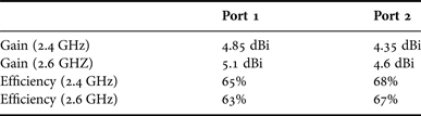
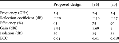
Figure 13 shows the measured efficiencies of the proposed MIMO antenna system from the frequency bandwidth of 1.5–3 GHz. It can be observed that, the 60% efficiency bandwidth is 2.1–2.7 GHz. Table 1 lists the measured gains and efficiencies of the microstrip-fed monopole antennas for both ports at 2.4 and 2.6 GHz when one port is excited and the other port is terminated with 50 Ω impedance matching. It is observed that, the gains from 4.35 to 5.1 dBi and efficiencies from 65 to 68% have been achieved. Table 2 lists the comparison between the results of the proposed MIMO antenna system and related works. It can be seen that the proposed antenna provides good performance in term of isolation and gain than other related works.
Fig. 13. Measured efficiency of the proposed MIMO antenna system.
Table 1. Measured gains and efficiencies of the microstrip-fed monopole antennas at 2.4 and 2.6 GHz.

Table 2. Comparison between the results of the proposed design and related works.
IV. CONCLUSION
In this paper a dual polarized wideband MIMO antenna system with common elements suitable for WAP application with operating frequency ranges from 2.3 to 2.9 GHz is proposed. The proposed MIMO antenna system comprises two orthogonal modes wideband microstrip-fed monopole antennas with a common radiated element and L-corner ground plane. Due to the structure of the ports the isolation between antenna elements is low. A new PE structure called CSPE is introduced to increase the isolation between the antennas. The reflection coefficient of less than −10 dB and isolation of more than 15 dB are achieved in the operating frequency range of 2.3–2.9 GHz. Also, the characteristics of the proposed MIMO antenna system include: polarization diversity, gain up to 5.1 dB, efficiency of up to 68%, diversity gain of approximately 10 dB while suppressing the ECC to below 0.15. The proposed MIMO antenna with the obtained results is suitable for WiFi (2.4 GHz) and LTE (2.6 GHz) WAP applications.
ACKNOWLEDGEMENTS
This research is supported by the Ministry of Science, Technology and Innovation Malaysia (MOSTI), the Ministry of Education Malaysia (MOE) and Universiti Teknologi Malaysia under Project Vote No. 4S079, 4F261 and 05H39.
Alishir Moradikordalivand received his B.S. and M.S. degrees in Electronic Engineering from the Arak Islamic Azad University, Iran in 2002 and 2005, respectively. He is currently pursuing his Ph.D. degree at the Faculty of Electrical Engineering, University of Technology Malaysia (UTM). His research interests are focused on wireless and mobile communication, antenna design, microwave active filters, LNA, VCO, Mixer, active inductor, ultra wide band, LNA, RF Application, and passive and active millimeter-wave devices. He is a member of IEEE and IEICE.
Chee Yen Leow obtained his B.Eng. degree in Computer Engineering from Universiti Teknologi Malaysia (UTM) in 2007. Since July 2007, he has been an academic staff in the Faculty of Electrical Engineering, UTM. In 2011, he obtained a Ph.D. degree from Imperial College London. He is currently a senior lecturer in the faculty and a member of the Wireless Communication Centre (WCC), UTM. His research interest includes but not limited to wireless relaying, MIMO, physical layer security, convex optimization, communications theory, and 5G.
Tharek Abd Rahman is a Director of Wireless Communication Centre, and Professor in the Faculty of Electrical Engineering, University Technology Malaysia. He received his B.Sc. degree in Electrical Engineering from the University of Strathclyde UK in 1979. Then, he obtained his Masters of Science in Communication Engineering from UMIST, Manchester, UK in 1982; and Doctor of Philosophy in Mobile Radio Communication from University of Bristol, UK in 1988. He is a member of: URSI, MIEEE, ITU, IEEE, and MCMC.
Sepideh Ebrahimi received her B.S. and M.S. degrees in Electronic Engineering from the Arak Islamic Azad University, Iran in 2004 and 2006, respectively. Currently, she is a lecturer of Aligoudarz Islamic Azad University. Her research interests are focused on wireless and mobile communication, antenna design, and microwave active filters, RFIC, passive and active millimeter-wave devices. Also she is a member of IEEE.
 Tien Han Chua received both the B.Sc. (Honours) degree in Electrical engineering and the Master of Electrical Engineering in Wireless Engineering from the Universiti Teknologi Malaysia in 2003 and 2007, respectively. He was a Tutor (2005–2007) and then a University Lecturer (2007–present) at the Faculty of Electrical Engineering, Universiti Teknologi Malaysia. He is currently pursuing his Ph.D. degree in wireless propagation at the Computer Laboratory, University of Cambridge. His research interests include broadband fixed wireless access systems, radio propagation, and channel modeling and measurement.