


Introduction
Substrate-integrated waveguide (SIW) integrates the characteristics of the uniplanar rectangular waveguide (RWG) and planar transmission lines, which establish an attractive trade-off between them [Reference Deslandes and Wu1]. During the past few years, a lot of microwave components and circuits have been realized in SIW technology, among which SIW power dividers with high isolation and broad bandwidth have attracted unique attention since they are highly desired in power-combining amplifiers and phased array antennas [Reference Zhang and Wu2–Reference Rave and Jacob6]. In [Reference Zhang and Wu2], a half-mode SIW (HMSIW) power divider with transverse electric – 20 (TE20) mode suppression achieved isolation over 10 dB with an operation frequency range of 18–35 GHz. However, its isolation is still not good enough and will be limited by the strong parasitic effect of the lumped resistor at a higher frequency. To overcome these drawbacks, another HMSIW power divider soldered the isolated resistor on the spacing slot between the two HMSIW branches [Reference Smith and Abhari3]. It achieves isolation over 15 dB from 9.5 to 13.5 GHz, corresponding to fractional bandwidth (FBW) of 35%. However, its isolation and output return loss swings with the value and location variations of the isolated resistor, which causes extra complexity. In [Reference Kazemi and Fathy4], an eight-way power splitter with over 65% FBW is implemented by utilizing the ridge SIW. However, its T-junction building block has no isolation inherently. A six-port power-dividing network shows the isolation of 20 dB over 12–16 GHz [Reference Liu and Xiao5]. Unfortunately, its phase imbalance can exceed 10° in several frequency ranges, and insertion loss at edges of its pass-band rolls off rapidly. Recently, a multilayer SIW power divider with embedded thick film resistive septum exhibits over 22 dB isolation over 18.5–22 GHz [Reference Rave and Jacob6]. Another SIW power divider integrated with thick film resistive layer even shows 40% FBW with 20 dB isolation [Reference Pasian, Silvestri, Rave, Bozzi, Perregrini, Jacob and Samanta7]. Nevertheless, their realization requires a costly and complex thick film fabrication process.
On the other hand, based on the similarity of their structures, the classical RWG works can provide promising ideas for the investigation of SIW technology. For instance, a six-port building block for power distribution and combination is proposed based on the Riblet coupler [Reference Alessandri, Giordano, Guglielmi, Martirano and Vitulli8, Reference Auld9]. Moreover, a modified five-port two-way RWG power divider with equal-ratio in in-phase power distribution operation has been developed in [Reference Ding, Wang, Zhang and Wang10]. Its SIW version incorporating absorbing material for impedance matching has even been briefly reported in [Reference Huang, Jiang, Jin, Zhou, Leng, Wang and Wu11]. However, both [Reference Ding, Wang, Zhang and Wang10, Reference Huang, Jiang, Jin, Zhou, Leng, Wang and Wu11] just shortly present their corresponding works, whereas none of them focused on the detailed theoretical analyses of this five-port power dividing/combining unit cell, which is inconvenient and incomprehensive for its further applications to other microwave components and circuits. In this paper, two wideband well-balanced SIW power dividers/combiners employing the five-port unit cell were used as reported in [Reference Ding, Wang, Zhang and Wang10]. Section “SIW power dividing/combining unit cell” detailed explains the basic transmission property of the five-port power combining/dividing unit cell with both theoretical analyses and numerical simulations. Subsequently, the design procedures of the prototypes and discussions on the experimental results are successively shown in Section “Experimental results”. Finally, a conclusion is given.
SIW power dividing/combining unit cell
Figure 1 sketches signal flows in the conventional Y-junction and the five-port power dividing/combining unit cell, in which the solid arrows denote power dividing operation and the dash arrows denote power combining operation. For the conventional Y-junction, the power dividing operation can achieve small reflection but bad isolation, while the power combining operation exhibits large reflection inherently, resulting in its unavailability for practical applications. However, for the five-port power dividing/combining unit cell, its operation principles will be much different owing to the influence from the two newly-added ports.
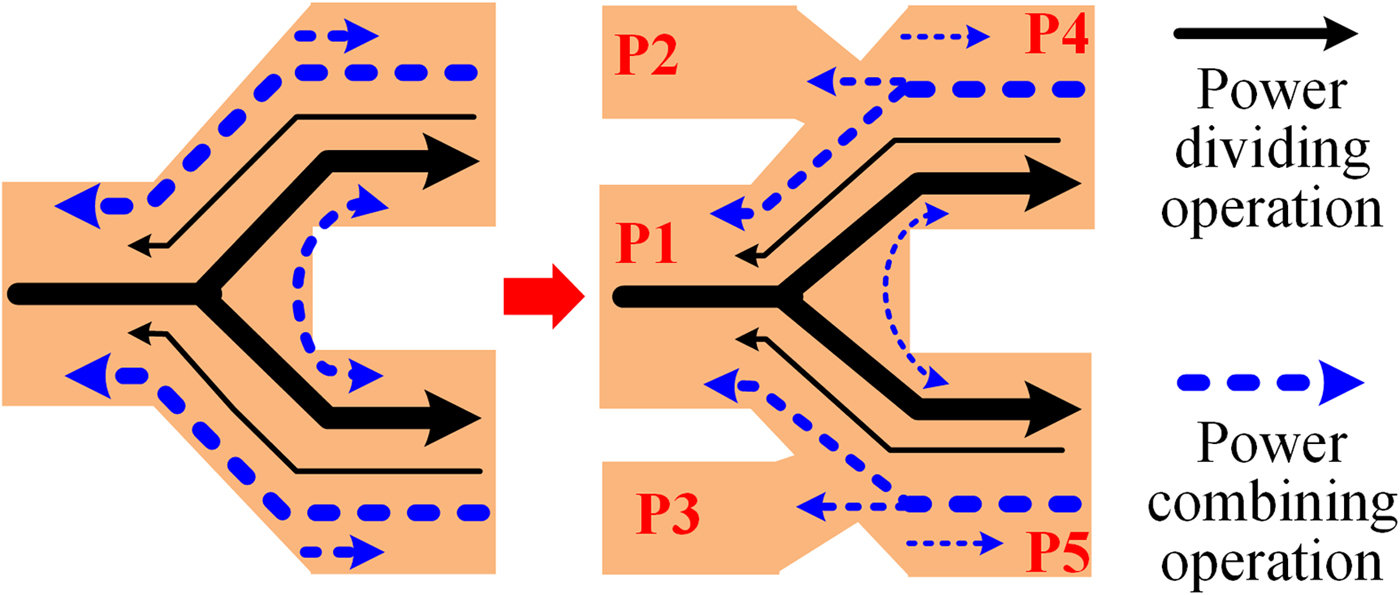
Fig. 1. Signal flows in the five-port power dividing/combining unit cell.
First of all, the basic properties of the five-port power dividing/combining unit cell are investigated on the basis of the microwave network theory. As is known, the scattering matrix of an arbitrary five-port unit cell can be expressed as
 $$\openup 4pt[S] = \left[ {\matrix{ {S_{11}} & {S_{12}} & {S_{13}} & {S_{14}} & {S_{15}} \cr {S_{21}} & {S_{22}} & {S_{23}} & {S_{24}} & {S_{25}} \cr {S_{31}} & {S_{32}} & {S_{33}} & {S_{34}} & {S_{35}} \cr {S_{41}} & {S_{42}} & {S_{43}} & {S_{44}} & {S_{45}} \cr {S_{51}} & {S_{52}} & {S_{53}} & {S_{54}} & {S_{55}} \cr}} \right].$$
If the five-port unit cell is passive and contains no anisotropic material, then it must be reciprocal and its scattering matrix will be symmetrical. In other words, S ij = S ji, and i ≠ j. And, if all the five ports are matched, then S ii = 0. So the scattering matrix will be as follows:
 $$\openup 4pt[S] = \left[ {\matrix{ 0 & {S_{12}} & {S_{13}} & {S_{14}} & {S_{15}} \cr {S_{12}} & 0 & {S_{23}} & {S_{24}} & {S_{25}} \cr {S_{13}} & {S_{23}} & 0 & {S_{34}} & {S_{35}} \cr {S_{14}} & {S_{24}} & {S_{34}} & 0 & {S_{45}} \cr {S_{15}} & {S_{25}} & {S_{35}} & {S_{45}} & 0 \cr}} \right].$$
Subsequently, as shown in Fig. 1, the five-port power dividing/combining unit cell is longitudinally axisymmetric along the center-line of port P1. That is, ports P2 and P4 are, respectively, symmetrical with P3 and P5. Then, S 12 = S 13, S 14 = S 15, S 24 = S 35, S 34 = S 25, and S 24 ≠ S 25, S 34 ≠ S 35. Hence, the scattering matrix is simplified as follows:
 $$\openup 4pt[S] = \left[ {\matrix{ 0 & {S_{12}} & {S_{12}} & {S_{14}} & {S_{14}} \cr {S_{12}} & 0 & {S_{23}} & {S_{24}} & {S_{25}} \cr {S_{12}} & {S_{23}} & 0 & {S_{25}} & {S_{24}} \cr {S_{14}} & {S_{24}} & {S_{25}} & 0 & {S_{45}} \cr {S_{14}} & {S_{25}} & {S_{24}} & {S_{45}} & 0 \cr}} \right].$$
Moreover, if the five-port unit cell is lossless, then ten independent equations can be obtained under the unitarity condition as below [Reference Pozar12, Reference Collin13]:
 $$\left\{ \matrix{S_{12}S_{12}^ {^\ast} + S_{12}S_{12}^ {^\ast} + S_{14}S_{14}^ {^\ast} + S_{14}S_{14}^ {^\ast} = 1, \hfill \cr S_{12}S_{12}^ {^\ast} + S_{23}S_{23}^ {^\ast} + S_{24}S_{24}^ {^\ast} + S_{25}S_{25}^ {^\ast} = 1, \hfill \cr S_{14}S_{14}^ {^\ast} + S_{24}S_{24}^ {^\ast} + S_{25}S_{25}^ {^\ast} + S_{45}S_{45}^ {^\ast} = 1, \hfill \cr S_{12}S_{23}^ {^\ast} + S_{14}S_{24}^ {^\ast} + S_{14}S_{25}^ {^\ast} = 0, \hfill \cr S_{12}S_{24}^ {^\ast} + S_{12}S_{25}^ {^\ast} + S_{14}S_{45}^ {^\ast} = 0, \hfill \cr S_{12}S_{12}^ {^\ast} + S_{24}S_{25}^ {^\ast} + S_{25}S_{24}^ {^\ast} = 0, \hfill \cr S_{12}S_{14}^ {^\ast} + S_{23}S_{25}^ {^\ast} + S_{25}S_{45}^ {^\ast} = 0, \hfill \cr S_{12}S_{14}^ {^\ast} + S_{23}S_{25}^ {^\ast} + S_{24}S_{45}^ {^\ast} = 0, \hfill \cr S_{12}S_{14}^ {^\ast} + S_{23}S_{24}^ {^\ast} + S_{24}S_{45}^ {^\ast} = 0, \hfill \cr S_{14}S_{14}^ {^\ast} + S_{24}S_{25}^ {^\ast} + S_{25}S_{24}^ {^\ast} = 0. \hfill} \right.$$
Then, by using the similar calculation processes introduced in [Reference Collin13], the ideal unitary scattering matrix of the five-port power dividing/combining unit cell is given as
 $$[S] = \displaystyle{1 \over 2}\left[ {\matrix{ 0 & 0 & 0 & {\sqrt 2} & {\sqrt 2} \cr 0 & 0 & {\sqrt 2} & 1 & j \cr 0 & {\sqrt 2} & 0 & j & 1 \cr {\sqrt 2} & 1 & j & 0 & 0 \cr {\sqrt 2} & j & 1 & 0 & 0 \cr}} \right].$$
According to (5), as the signal inputs the five-port unit cell from port P1, ports P4 and P5 will receive equal power while no output can be received at ports P2 and P3. Meanwhile, ports P4 and P4 are isolated. Therefore, the five-port unit cell can be utilized to develop a highly isolated two-way power divider/combiner.
Meanwhile, it has been well known that the physical sizes of SIW components and circuits are much more compact than their corresponding RWG counterparts, which are mainly due to the planarization of their structure and the increasing permittivity of their substrates. Hence, to extend the availability and practicability of the five-port unit cell in microwave systems, especially in the system integration and packaging, the SIW technology is selected as the implementation platform.
Figure 2 shows the geometry and equivalent-circuit models of the five-port SIW dividing/combining unit cell, which can be further studied by using the even–odd mode analysis method. In Fig. 2(a), the area between cross-sections XX′ and YY′ denotes the coupling region, with width wc and length lc, respectively. According to Fig. 2(b), once Ports P4 and P5 are driven by in-phase signals, the five-port SIW unit cell is under even–mode operation and its longitudinal symmetrical line can be equivalent as the magnetic wall. With the structure symmetry, as the in-phase waves of the TE10 mode in P4 and P5 propagate in the coupling region, only the even-distributed modes such as TE10, TE30, and TE50 modes can be excited. And after propagating through XX″, the higher-order TE30 and TE50 modes will be cutoff whereas only the TE10 mode can be supported. Meanwhile, the remained signals will remain in-phase so that to add up with each other at P1 but are out-of-phase and consequently subtracted at P2 and P3. On the other hand, for the odd-mode case in Fig. 2(c), as two out-of-phase signals input the unit cell from P4 and P5 separately, the longitudinal symmetrical line will perform like the electrical wall. Therefore, as the out-of-phase waves of TE10 mode propagate in the coupling region, they will excite the odd-distributed TE20 and TE40 modes, which will be cut-off after crossing over XX′. Due to the influence of the electrical wall, port P1 will be cut into two narrower waveguides so that all modes will be cutoff. Hence, no output can be captured at P1. On the contrary, signals coming from P4 and P5 will be fed into P2 and P3. Additionally, as a signal inputs the five-port SIW unit cell from P1, only the even-distributed TE10, TE30 and TE50 modes can be excited in the coupling region, which can be deduced from the reciprocity of the unit cell, or inferred from its structure symmetry. In a word, the five-port SIW unit cell can act as a two-way in-phase power divider/combiner. Meanwhile, it will also be useful in the separation of the differential- and common-mode coefficients of signals.
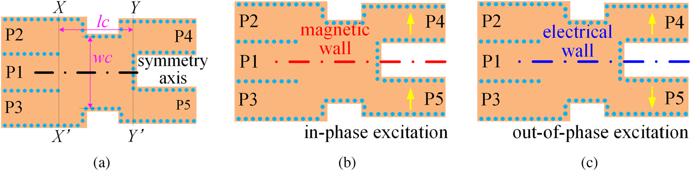
Fig. 2. (a) Geometry, (b) even-mode equivalent-circuit model, and (c) odd-mode equivalent-circuit model of the five-port SIW power dividing/combining unit cell.
Afterwards, it is important to discuss the size determination of the five-port SIW unit cell. Firstly, widths of the five ports are mainly determined by the operation frequency range. Generally, the cutoff frequency of the dominant mode determined by the SIW width is supposed to be lower than the lowest operation frequency. Based on the operation frequency range, widths of the five SIW ports can be selected rapidly. Secondly, the width of the coupling region, wc, is mainly determined by the number of transmissible modes in the coupling region. Typically, only the single TE10 mode or TE10/TE30 modes are suitable for low-loss transmission. Based on the SIW theory, the cut-off wavelengths of TE10, TE30 and TE50 modes are as follows:
 $$\eqalign{\lambda _{c \hyphen 10} = \,& {{2\pi} / {k_{c \hyphen 10} = 2a_{SIW}}}, \cr \lambda _{c \hyphen 30} = \,& {{2\pi} / {k_{c \hyphen 30} = {{2a_{SIW}} / 3}}}, \cr \lambda _{c \hyphen 50} = \,& {{2\pi} / {k_{c \hyphen 50} = {{2a_{SIW}} / 5}}}.} $$
where a SIW is the equivalent width of SIW and can be calculated by a SIW = a–4.32R 2/p + 0.4R 2/a, in which R is the radius of metallic vias and p is the center-to-center spacing of adjacent vias.
If only TE10 mode is transmissible in the coupling region, the guided wavelength λ g should satisfy:
 $$\lambda _{c \hyphen 30} \lt \lambda _g \lt \lambda _{c \hyphen 10} \Rightarrow 0.5\lambda _g \lt a_{SIW} \lt 1.5\lambda _g.$$
If both TE10 and TE30 modes are supported in the coupling region, it can be obtained that
 $$\lambda _{c \hyphen 50} \lt \lambda _g \lt \lambda _{c \hyphen 30} \Rightarrow 1.5\lambda _g \lt a_{SIW} \lt 2.5\lambda _g.$$
Therefore, once the permitted modes in the coupling region are selected, a can be determined.
Thirdly, length of the coupling region, lc, is also mainly determined by the number of permitted modes in it. If only the TE10 mode is permitted in the coupling region, its electric (E)-field magnitude in the middle is much stronger than that at both edges. After propagating from XX″ to YY″, the E-field magnitude of the TE10 mode around the metallic vias in the middle of YY″ is still much stronger than that at both edges, which consequently causes strong input reflection. Hence, only supporting the TE10 mode in the coupling region can achieve short lc, but also result in bad input return loss. On the other hand, if both TE10 and TE30 modes are transmissible, the situation will be much different. As depicted in [Reference Ding, Wang, Zhang and Wang10, Reference Huang, Jiang, Jin, Zhou, Leng, Wang and Wu11], after propagating through the same length lc, TE10 and TE30 modes are with electrical lengths of θ 10 and θ 30, which are given as
 $$\theta _{10} = \beta _{10} \cdot lc,\quad \theta _{30} = \beta _{30} \cdot lc,$$
where β 10 and β 30 are the phase constants of TE10 and TE30 modes, respectively.
As TE10 and TE30 modes arrive at YY′, they are supposed to be out-of-phase in the middle but in-phase at both edges. Being out-of-phase in the middle means the two modes will subtract, thus decreasing the strength of the E-field near the metallic vias in the middle and ultimately decreasing the input reflection. Meanwhile, being in-phase at both edges will make the TE10 and TE30 modes add up together so that more electromagnetic (EM) energy can be fed into the dividing ports. Hence, transmission with both TE10 and TE30 modes in the coupling region is better than that with the single TE10 mode. To perform such an operation, θ 10–θ 30 should satisfy
 $$\theta _{10} - \theta _{30} = 2(n - 1)\pi, $$
where n is a positive integer. Then, lc is calculated as
 $$lc = (2n - 1)\pi /(\beta _{10} - \beta _{30}) = \pi /(\beta _{10} - \beta _{30}).$$
Here n is set as 1 for size reduction.
Furthermore, it is necessary to realize that the above calculations are in allusion to single frequency operation. In order to avoid the steep and acute change of wave propagation caused by the discontinuities in the five-port SIW unit cell, some matching structures and transitions are essential to be employed to improve the impedance matching performance, so that to broaden the operation bandwidth. Therefore, the taper-shaped SIW structure is introduced into the five-port SIW power dividing/combining unit cell, and the modified geometry is illustrated in Fig. 3.

Fig. 3. Geometry of the five-port SIW power dividing/combining unit cell with taper-shaped transition structure.
Thereafter, to demonstrate the aforementioned theoretical analyses, some full wave EM simulations are carried out on the five-port SIW power dividing/combining unit cell by using the commercial finite-element-method-based simulator. In all simulations, the substrate is set with a thickness of 0.508 mm, relative permittivity of 2.94, and dielectric loss tangent of 0.0012. The copper metal is selected as the surface conductor, with a thickness of 0.035 mm. Moreover, geometrical parameters corresponding to Fig. 3 are l1 = l2 = l3 10, w1 = w2 = w3 = 8, lc = 6, wc = 18, s = 2, p = 0.8, R = 0.2 (unit: mm). Figure 4 shows the simulated E-field distributions of the five-port SIW unit cell at 16 GHz under various excitations. According to Fig. 4(a), as the five-port SIW unit cell is excited from P1, most of the EM energy will propagate through the coupling region and into P4 and P5 eventually, whereas only little EM energy propagates to P2 and P3. So the unit cell can be utilized as a two-way power divider, and P1 and P2/P3 are well-isolated as well. Subsequently, as shown in Fig. 4(b), once a signal inputs the unit cell from P5, ports P1, P2, and P3 will receive signal with various strengths. Meanwhile, seldom signal energy can be captured at P4, which means good isolation between P4 and P5. Thirdly, as the unit cell is simultaneously excited with in-phase signals at P4 and P5, P1 will get much stronger EM energy, while little EM energy can be obtained at P2 and P3, as depicted in Fig. 4(c). That is to say, the unit cell can act as an in-phase power combiner. Finally, from Fig. 4(d), with simultaneously out-of-phase inputs from P4 and P5, almost all of the EM energy propagates through P2 and P3, whereas nearly no signal can be detected at P1. Hence, it can be predicted from Figs 4(c) and 4(d) that the five-port SIW unit cell can be utilized to separate the differential- and common-mode coefficients of signals.

Fig. 4. E-field distribution of the unit cell in Fig. 3 at 16 GHz under various excitations. (a) Excitation from P1, (b) excitation from P5, (c) simultaneously in-phase excitation from P4 and P5, and (d) simultaneously out-of-phase excitation from P4 and P5.
Particularly, as sketched in Figs 4(a) and 4(c), there is still some leakage at P2 and P3, which can cause extra insertion loss in even mode. Hence, the total insertion loss of the five-port SIW power dividing/combining unit cell will consequently increase. To verify this prediction, powers of the output, the loss and leakage are investigated. Here, the output means the sum value of P4 and P5. The loss contains the dielectric loss, conductivity loss, and radiation loss, while the leakage only means output power obtained at the two isolated ports. Consider the original input power at P1 is 1, then it can be further captured from the full-wave simulation that the power relationship at 16 GHz
 $$P_i\!\!:\!\!P_o\!\!:\!\!P_{loss}\!\!:\!\!P_{leak} = 1\!\!:\!\!0.91\!\!:\!\!0.055\!\!:\!\!0.035,$$
where P i, P o, P loss, and P leak denote input, output, loss and leakage powers, respectively.
It can be obtained from (12) that P leak is comparable with P loss, which means the leakage at isolated ports P2 and P3 can introduce extra loss to the whole unit cell. To overcome this issue, the size of the coupling region should be tuned carefully for the specific frequency. The taper transition can be modified slightly to keep low leakage and broadband simultaneously as well.
Finally, to illustrate the contribution from the newly-added ports visually, Fig. 5 shows the simulated isolations and output return losses of the Y-junction and the five-port SIW power dividing/combining unit cell. As shown in Fig. 5, both isolation and output return loss of the five-port SIW unit cell have been improved a lot as compared with the Y-junction. Obviously, by introducing the two isolated ports into the Y-junction, both the isolation and output return loss are enhanced effectively with the utilization of the two extra isolated ports.
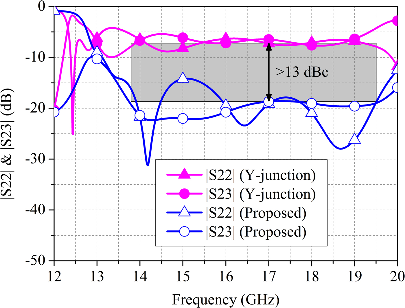
Fig. 5. Simulated isolations and output return losses of the conventional SIW Y-junction and the derived five-port SIW power combining/dividing unit cell.
In addition, it is worth mentioning that design processes of the five-port SIW power dividing/combining unit cell is simpler than those of the corresponding RWG counterpart. As depicted in [Reference Deslandes and Wu1, Reference Zhang and Wu2], SIW only supports TEm0 modes, for instance, the TE10, TE20 and TE30 modes. Based on equations (6)–(11) listed above, it is quite easy to control the existence of these three modes in practical designs. However, in RWG, both TE and transverse magnetic (TM) modes can be supported. Obviously, controlling the existence of TE and TM modes in RWG is much more complex and difficult than controlling the TEm0 modes in SIW. Therefore, as the five-port power dividing/combining unit cell is implemented in SIW, its design processes can be much simpler and more efficient. Furthermore, for an SIW with an equivalent width of a SIW, cutoff frequencies of the TE10 and TE20 modes in it are
 $$f_{c \hyphen 10} = \displaystyle{1 \over {2\sqrt {\mu \varepsilon}}} \cdot \sqrt {{\left( {\displaystyle{1 \over {a_{SIW}}}} \right)}^2 + {\left( {\displaystyle{0 \over h}} \right)}^2} = \displaystyle{1 \over {2a_{SIW}\sqrt {\mu _r\mu _0\varepsilon _r\varepsilon _0}}}, $$
 $$f_{c \hyphen 20} = \displaystyle{1 \over {2\sqrt {\mu \varepsilon}}} \cdot \sqrt {{\left( {\displaystyle{2 \over {a_{SIW}}}} \right)}^2 + {\left( {\displaystyle{0 \over h}} \right)}^2} = \displaystyle{1 \over {a_{SIW}\sqrt {\mu _r\mu _0\varepsilon _r\varepsilon _0}}}, $$
where μ 0 and ε 0 are the permeability and permittivity in free space, μ r and ε r are the relative permeability and permittivity of the substrate in SIW, and h represents the substrate thickness.
From (13) and (14), 2·f c-10 = f c-20, then the single mode operation bandwidth in SIW is
 $$BW_{SIW} = f_{c \hyphen 10} - f_{c \hyphen 20} = \displaystyle{1 \over {2a_{SIW}\sqrt {\mu _r\mu _0\varepsilon _r\varepsilon _0}}}. $$
For an RWG with inter cross-section size of a × b (a > b), cutoff frequencies of the TE10, TE01, and TE20 modes in it are
 $$f_{cs \hyphen 10} = \displaystyle{1 \over {2\sqrt {\mu \varepsilon}}} \cdot \sqrt {{\left( {\displaystyle{1 \over a}} \right)}^2 + {\left( {\displaystyle{0 \over b}} \right)}^2} = \displaystyle{1 \over {2a\sqrt {\mu _0\varepsilon _0}}}, $$
 $$f_{cs \hyphen 01} = \displaystyle{1 \over {2\sqrt {\mu \varepsilon}}} \cdot \sqrt {{\left( {\displaystyle{0 \over a}} \right)}^2 + {\left( {\displaystyle{1 \over b}} \right)}^2} = \displaystyle{1 \over {2b\sqrt {\mu _0\varepsilon _0}}}, $$
 $$f_{cs \hyphen 20} = \displaystyle{1 \over {2\sqrt {\mu \varepsilon}}} \cdot \sqrt {{\left( {\displaystyle{2 \over a}} \right)}^2 + {\left( {\displaystyle{0 \over b}} \right)}^2} = \displaystyle{1 \over {a\sqrt {\mu _0\varepsilon _0}}}. $$
According to (16)–(18), 2·f cs-10 = f cs-20, then the single mode operation bandwidth in RWG is
 $$BW_{RWG} = \left\{ \matrix{\,f_{c \hyphen 20} - f_{c \hyphen 10} = \displaystyle{1 \over {2a\sqrt {\mu _0\varepsilon _0}}}, \quad \quad \quad \,\,\,\,a \gt 2b, \hfill \cr f_{c \hyphen 01} - f_{c \hyphen 10} = \displaystyle{1 \over {2\sqrt {\mu _0\varepsilon _0}}} \left( {\displaystyle{1 \over b} - \displaystyle{1 \over a}} \right),\quad a \lt 2b. \hfill} \right.$$
As SIW and RWG are with the same dominant cutoff frequency, i.e. f c-10 = f cs-10, then f c-20 = f cs-20. Considering these conditions with (15) and (19) together, it can be obtained that  $BW_{RWG} \le BW_{SIW} $, so the single mode operation bandwidth of RWG is no larger than that of SIW.
Experimental results
SIW power divider/combiner with coaxial terminations
For an experimental proof of the aforementioned analysis, a 3 dB power divider/combiner prototype is designed. A detailed configuration of the SIW power combiner/divider is shown in Fig. 3. A Rogers RT/duroid 6002 substrate with a dielectric constant of 2.94 ± 0.04, loss tangent of 0.0013, thickness of 0.508 mm, and conductor thickness of 0.035 mm is used for design. Width and length of the coupling region, as well as the width of the five ports, are set up based on the conditions mentioned in Section “SIW power dividing/combining unit cell”. Subsequently, five taper transitions, with different widths and lengths, are also added between the 50 Ω microstrip lines and SIW ports to achieve optimized standing-wave performance at each port, respectively. Finally, the overall structure with SubMiniature version A (SMA) connectors is modeled and simulated by using the same commercial full-wave simulation software mentioned above. The optimized dimensions are listed in Fig. 6 as well.

Fig. 6. Detailed configuration and optimized dimensions of the SIW power divider/combiner with coaxial terminations.
SIW power divider/combiner with lumped resistors
Thereafter, since the SIW power divider/combiner with coaxial termination is inconvenient for the printed circuit board (PCB)-level integration with other planar circuits, another experiment is done to remove the coaxial terminations by the 50 Ω lumped resistors. Most of the design procedures are exactly same as those in the coaxial one. Particularly, a 50 Ω microstrip line is connected between the isolated port and the lumped resistor, with several vias placed at the other port of lumped resistors for grounding. Afterwards, length of the microstrip line and size of the grounded vias are both tuned to optimize the impedance matching performance. Finally, this prototype is simulated by using the same aforementioned simulator as well, with its optimized dimensions given in Fig. 7.
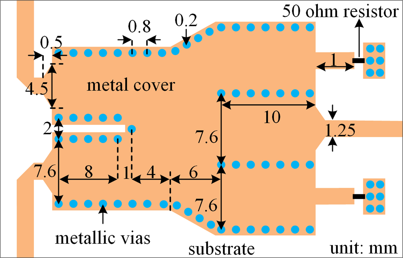
Fig. 7. Detailed configuration and optimized dimensions of the SIW power divider/combiner with lumped resistors.
Experimental results and discussions
The two designed prototypes are fabricated by using the standard PCB process. A Rogers RT/duroid 6002 substrate with the same parameters in Section “SIW power dividing/combing unit cell” is utilized for fabrication. After fabrication, all five ports of the prototype are soldered with SMA coaxial connectors. Two coaxial terminations are connected to the isolated ports of the first prototype, and two 50 Ω lumped resistors with 0603 assembly form are silver soldered to the second prototype with the silver–copper–zinc composite alloys. The measurement is carried out by using an Agilent E8363C vector network analyzer, with the default short-open-load-thru calibration is utilized to remove the influence from the coaxial cables. The thru-reflect-line (TRL) calibration is not used since the three-port TRL calibration is much more complex than the two-port case, therefore, the influence of the SMA connectors on the phase and amplitude balance and insertion losses is unable to be removed. Figure 8 shows the simulated and measured results of the prototype with coaxial terminations, with the photograph shown in the inset. As shown in Fig. 8(a), input and output return losses of the fabricated power combiner/divider with coaxial terminations are both over 10.5 dB. Meanwhile, its insertion losses are about 4.5 ± 0.5 dB, and the isolation is better than 17.5 dB from 13.8 to 19.5 GHz, corresponding to FBW of 33%, as shown in Fig. 8(b). Moreover, it can also be obtained from Fig. 8(c) that the measured amplitude imbalance is less than ±0.4 dB and the measured phase imbalance is less than ±2.5°.

Fig. 8. Simulated and measured results of the fabricated SIW power divider/combiner with coaxial terminations. (a) Input and output return losses; (b) insertion losses and isolation; (c) phase and amplitude imbalances; (d) photograph of the fabricated prototype.
On the other hand, a comparison between the simulated and measured results of the fabricated prototype with lumped resistors is shown in Fig. 9, as well as its photograph. According to Fig. 9(a), the measured input return loss of the fabricated SIW power divider/combiner with lumped resistors is better than 13 dB, and the output ones are over 10 dB. Moreover, from Fig. 9(b), the measured isolation is over 16 dB from 14.5 to 19 GHz, and the insertion losses are about 4.8 ± 0.5 dB from 14 to 18 GHz, corresponding to an FBW of 25%. Meanwhile, the measured amplitude and phase imbalances are about ±0.5 dB and less than ±3°, respectively, which are given in Fig. 9(c).
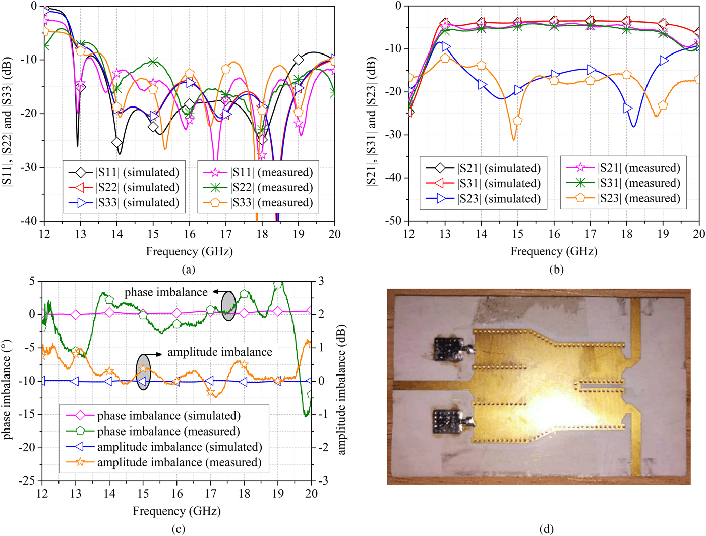
Fig. 9. Simulated and measured results of the fabricated SIW power divider/combiner with lumped resistors. (a) Input and output return losses; (b) insertion losses and isolation; (c) phase and amplitude imbalances; (d) photograph of the fabricated prototype.
Table 1 summarizes the comparison between some reported similar SIW power dividers and the presented ones. Compared with the two-way power divider in [Reference Smith and Abhari3], the presented ones are with lower amplitude imbalance, with similar insertion loss and phase imbalance. Compared with the three-way power divider in [Reference Liu and Xiao5], the presented ones are with better amplitude and phase balance performance. Even though the power divider in [Reference Rave and Jacob6] is with lower insertion loss and similar amplitude imbalance, its FBW is much narrower, and its thick film fabrication is expensive and complex. Based on all the comparison mentioned above, the proposed SIW power dividers/combiners achieve a good trade-off between bandwidth, isolation, insertion loss, phase, and amplitude imbalances. Moreover, the five-port power dividing/combining unit cell has provided a new building-block to set up waveguide power dividers.
Table 1. Comparison between some reported similar SIW power dividers and the presented works

a Results of the three-way power divider.
Conclusion
Two 3 dB H-plane wideband high-isolated SIW power combiners/dividers with well-balanced performance are developed. A 17.5 dB-isolation FBW of 33% and a 16 dB-isolation FBW of 25% are achieved by the two prototypes, respectively, as well as good phase and amplitude balances. Compared with some reported works realized in the same technology, the proposed one with coaxial termination exhibits a wider bandwidth for the same isolation performance, as well as similar insertion loss, phase, and amplitude balance. The proposed one with lumped resistors also shows a similar performance as the references. Therefore, the proposed SIW power dividers/combiners are promising to be utilized in the wideband phased array antennas and power-combining amplifiers applications in the future wireless communication and radar systems.
Acknowledgements
This work was supported in part by the National Science and Technology Major Project under grant no. 2016ZX03001022-004, the National Science Foundation of China under grant no. 61601087, and the Fundamental Research Funds for Central Universities under grant no. ZYGX2016004.
 Yong Mao Huang received the B.S. degree in Communication Engineering and a Ph.D. degree in Communication and Information Systems from the University of Electronic Science and Technology of China (UESTC), Chengdu, China, in 2010 and 2017, respectively. From 2014 to 2015, he was with the Department of Electrical Engineering, University of South Carolina, Columbia, SC, USA. Since 2018, he has been an Assistant Professor at the School of Electrical and Electronic Information, Xihua University, Chengdu, China. His research interests include radiofrequency/microwave/millimeter-wave circuits and systems for wireless communication, radar and sensing applications, substrate-integrated circuits and antennas, and reconfigurable components. He has authored and coauthored over 40 referred papers. He serves as a reviewer for various IEEE, IET and ACES journals, transactions and letters. He has served as the Technical Program Committee Member of the 2018 IEEE MTT-S International Conference on Microwaves in Mobility (ICMIM 2018) in Munich, Germany, and several other international conferences/symposia.
 Haiyan Jin received the B.S. degree in Electronic Information Technology, M.S. and Ph.D. degrees in Electrical Engineering from the University of Electronic Science and Technology of China in 2001, 2006 and 2010, respectively. From 2013 to 2014, he was a postdoc at the Poly-Grames Research Center, École Polytechnique de Montreal, University of Montreal, Montreal, QC, Canada, where he focused on the beam-forming antennas. Since 2010, he has been at the School of Information and Communication Engineering, University of Electronic Science and Technology of China (UESTC), Chengdu, China, where he is now Associate Professor. His current research interests include the antenna array designs and substrate-integrated techniques for microwave and millimeter-wave communication systems. He has authored or coauthored over 70 referred papers. He is a reviewer of several IEEE and IET journals, transactions and letters. He has also served as Technical Program Committee members and Session Chairs for various international conferences.
 Yuliang Zhou received the B.S. degree in Applied Physics from the University of Electronic Science and Technology of China, Chengdu, China, in 2012, where he is currently pursuing Ph.D. degree. Since September 2017, he has been with the Microwave Laboratory, Department of Electrical, Computers and Biomedical Engineering, University of Pavia, Pavia, Italy as a visiting Ph.D. student. His current research interests include substrate-integrated circuits, leaky-wave antennas, hybrid oscillators and resonance-based sensing systems. He has authored over 10 publications in referred journals and international conferences/symposia. He has served as a reviewer for several peer-reviewed periodicals and international conferences/symposia.
 Supeng Leng received the Ph.D. degree from Nanyang Technological University (NTU), Singapore. He was a Research Fellow of the Network Technology Research Center, NTU. He is currently a Professor and Vice Dean of the School of Information and Communication Engineering, University of Electronic Science and Technology of China, Chengdu, China. His current research interests include resource, spectrum, energy, routing and networking in the Internet of Things, vehicular networks, broadband wireless access networks, smart grid, and the next generation mobile networks. He has authored over 150 publications in referred journals and international conferences/symposia. He has served as Organizing Committee Chair, Technical Program Committee Chair/Member for many international conferences, as well as a reviewer for over 10 international peer-reviewed journals.
 Maurizio Bozzi received the Ph.D. degree from the University of Pavia (Italy) in 2000. He held research positions with various universities worldwide, including Technische Universität Darmstadt (Germany), Universitat de Valencia (Spain), École Polytechnique de Montréal (Canada) and Tianjin University (China). He is currently an Associate Professor at the University of Pavia. His main research interests include computational electromagnetics, substrate-integrated waveguide technology, and novel materials and fabrication technologies for microwave circuits (including paper, textile, and 3D printing). He is a Fellow of the IEEE. He is an Elected Member of the Administrative Committee of the IEEE Microwave Theory and Techniques Society and was a Member of the General Assembly of the European Microwave Association. He is an associate editor for IEEE Microwave and Wireless Components Letters, Electronics Letters, and IET Microwaves, Antennas and Propagation. He was the General Chair of IEEE IMWS-AMP 2017, IEEE NEMO 2014, and IEEE IMWS-MWIT 2011.


