


Introduction
With the rising evolution of wireless communication technology, more and more researchers are focused on the fifth generation (5G) wireless systems. Reducing energy consumption will be one of the greatest challenges for the next generation of communication technology. Another important issue is the broadband requirement from multi-band multi-mode wireless communication systems. As the primary energy-dissipation device, wideband high efficiencypower amplifier (PA) is worth studying [Reference Saad, Fager, Cao, Zirath and Andersson1–Reference Tuffy, Guan, Zhu and Brazil5]. In [Reference Saad, Fager, Cao, Zirath and Andersson1, Reference Ding, He, You, Xie and Hu2], the optimum source and load impedances across 2 GHz bandwidth were obtained, and a systematic approach was presented to design wideband matching network. The adjacent channel leakage ratios (ACLRs) after digital pre-distortion (DPD) linearization with 20 MHz LTE modulated signal at 2.5 GHz was −44 dBc in [Reference Saad, Fager, Cao, Zirath and Andersson1], and the ACLRs after DPD linearization with 5 MHz WCDMA signal at 3 GHz was −45.3 dBc in [Reference Ding, He, You, Xie and Hu2]. In [Reference Arnous, Zhang, Barbin and Boeck3], a new output matching network (OMN) including a 4:1 planar Guanella transformer was proposed to realize the wideband operation requirement and less information about the linearity of the proposed PA was given. In [Reference Shi, He, Li, Qi and Liu4, Reference Tuffy, Guan, Zhu and Brazil5], continuous PA theory on Class-B/J mode and Class-F mode was proposed to design broadband high-efficiency PAs. Although a high-efficiency continuous linearized Class-F PA was presented in [Reference Tuffy, Guan, Zhu and Brazil5], little discussion on how to improve the linearity was given. Most researchers were focused on developing wideband high-efficiency PAs [Reference Saad, Fager, Cao, Zirath and Andersson1–Reference Tuffy, Guan, Zhu and Brazil5], while high linearity of wideband PAs was given less attention.
To develop a high-linearity PA, reducing memory effects and third-order inter-modulation distortions (IMD3) is very critical [Reference Vuolevi and Rahkonen6–Reference Ghannouchi, Hammi and Helaoui8]. In a practical circuit, such as the Case 1 in Fig. 1, IMD3 is asymmetric due to strong memory effects. As a rule, DPD linearization technique depends on a stable nonlinear response, and it is degraded mainly by the memory effects [Reference Vuolevi and Rahkonen6]. Memory effects can be divided into two categories: electro-thermal memory effects and electrical memory effects [Reference Vuolevi and Rahkonen6–Reference Ghannouchi, Hammi and Helaoui8]. The electro-thermal memory effects are primarily attributed to a temperature change of the transistor junction [Reference Ghannouchi, Hammi and Helaoui8] and usually impacts low-frequency components of the signal in the megahertz range [Reference Vuolevi and Rahkonen6]. Compared with electro-thermal memory effects, the electrical memory effects are more significant for a wideband modulated signal [Reference Liu, Boumaiza, Sesay and Ghannouchi7]. Some methods have been presented to reduce the memory effects and improve the linearity [Reference Kim, Moon, Kim, Kim and Kim9–Reference Ladhani, Jones and Bouisse11]. In [Reference Kim, Moon, Kim, Kim and Kim9], an envelope short matching network was proposed at active ports to minimize the memory effects. This method is more suitable for narrow-band PA. A simple cascaded third-order analog pre-distorter can be applied to cancel third- and fifth- intermodulation distortions for designing wideband high-linearity PA [Reference Lee, Lee, Kam and Jeong10]. However, the insertion losses of an analog pre-distorter can degrade power added efficiency (PAE). The video bandwidth is closely related to the memory effects of wideband PAs. In [Reference Ladhani, Jones and Bouisse11], a high-k capacitor was used to adjust the envelope frequency response of the drain node impedance for improving the instantaneous bandwidth capability of RF power transistor. However, this was realized at the transistor-design-level. Hence, it is essential to develop wideband PA when high linearity and high efficiency are taken into account at the same time.

Fig. 1. Typical third-order intermodulation figure by two-tone signal testing (10 MHz tone spacing) with strong (Case 1) and weak (Case 2) memory effects (the same PA with two different drain bias networks).
In this paper, an analytical method is presented, which provides a methodology to reduce the memory effects and IMD3 for designing wideband high-efficiency linearized PAs. For the wideband PAs discussed in this work, only the electrical memory effects are considered. The analysis on the memory effects and IMD3 is given in the section “Analysis on memory effects and IMD3”. An improved Chebyshev low-pass matching network is proposed and realized in the section “Low-memory matching network design”. To validate the proposed approach, a wideband PA prototype is designed, fabricated, and measured in the section “PA design and measured results”.
Analysis on memory effects and IMD3
The generation mechanism of IMD3 is analyzed based on an assumption that the modeling of RF power transistor is simplified as a cascade of two nonlinear systems, G and H, as shown in Figure 2.5 of [Reference Ghannouchi, Hammi and Helaoui8]. Each of the two nonlinear systems is modeled by a third-degree polynomial model in (2.3) of [Reference Vuolevi and Rahkonen6] by considering the nonlinearity in the order of three. In Fig. 2, the envelope components G 0(|ω1 − ω2|), fundamental components G 1(ω1), G 1(ω2), second-harmonic components G 2(2ω1), G 2(2ω2) present the output of the first nonlinear system, G. These output of the first nonlinear system is considered as the input of the second nonlinear system, H. Then, IMD3 is generated at the output of the second nonlinear system, H. For example, the envelope signal |ω1 − ω2| and the upper two-tone signal ω2 are mixed in the quadratic nonlinearity of the second nonlinear system, H, which results in the generation of upper IMD3, H IM3,upper1. Similarly, the second-harmonic of the upper input signal 2ω2 and the lower two-tone signal from the negative frequency side −ω1 are mixed to generate the upper IMD3, H IM3,upper2. Moreover, the third-order nonlinearity G IM3 of the first system, G, passes through the linear response H 1 of the second system, H [Reference Ghannouchi, Hammi and Helaoui8]. As a result, the third-order intermodulation distortions of upper sideband, IMD3upper, can be expressed as:
 $$IMD3_{upper} = {H_1} {\ast} {G_{IM3}} + {H_{IM3,upper1}} + {H_{IM3,upper2}}.$$
Similarly, the third intermodulation distortions of lower sideband, IMD3lower, can be given by:
 $$IMD{3_{lower}} = {H_1} {\ast} {G_{IM3}} + H_{IM3,lower1} + H_{IM3,lower2} .$$
Obviously, IMD3 in (1) and (2) are affected not only by the fundamental voltage waveforms of the nodes, Z GG and Z DD, but also by the voltage waveforms at the envelope and second-harmonic frequencies, |ω 1 − ω 2|, 2ω 1 and 2ω 2. Z GG, and Z DD are indicated in Fig. 3. The key to reduce IMD3 is to control the frequency components and the voltage waveforms of the nodes, Z GG and Z DD. IMD3 can be minimized not only by optimizing the fundamental impedance but also by optimizing the out-of-band terminal node impedances, such as the envelope impedances and the second-harmonic impedances.
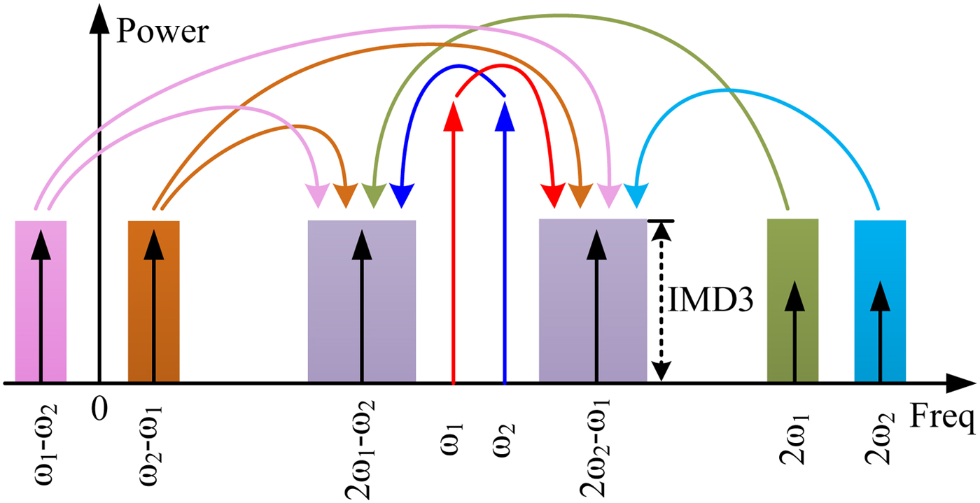
Fig. 2. Generation mechanism schematic of IMD3.

Fig. 3. Schematic diagram of wideband PA.
The electrical memory effects are mainly attributed to the variations of the frequency-dependent envelope, fundamental, and second-harmonic impedances of the terminal nodes, Z GG and Z DD. The memory effects can be minimized by optimizing the terminal node impedances Z GG and Z DD [Reference Vuolevi and Rahkonen6, Reference Ghannouchi, Hammi and Helaoui8]. The fundamental impedance can easily be kept constant by using wideband matching technique [Reference Saad, Fager, Cao, Zirath and Andersson1–Reference Tuffy, Guan, Zhu and Brazil5]. In [Reference Vuolevi and Rahkonen6, Reference Ghannouchi, Hammi and Helaoui8], the bias impedances Z G,bias and Z D,bias are excluded from the matching impedance Z G,match and Z D,match. However, this method is more suitable for narrow-band PA. A wideband PA usually needs high input impedance for bias network to suppress RF signal in a large bandwidth. Hence, Z G,bias and Z D,bias can be included in Z G,match and Z D,match and then the matching network provides the bias impedance, as shown in Fig. 3. The influence from the second-harmonic terminal node impedances can be reduced by employing low-pass matching network. Fortunately, Chebyshev low-pass matching technique [Reference Chen and Peroulis12] can provide constant fundamental impedances and very high second-harmonic impedances. When the fundamental and second-harmonic impedances play a minor role after the Chebyshev low-pass matching network is used, memory effects are for the most part produced by the envelope impedances. The terminal node impedances, Z GG and Z DD, at envelope frequency (|ω 1 − ω 2|) are calculated as follows:
 $$Z_{GG} \left({\left \vert {{\omega _1} - {\omega _2}} \right \vert} \right) = {Z_{G,device}} \bigg \Vert {Z_{G,match}},$$
 $$Z_{DD} \left({\left \vert {{\omega _1} - {\omega _2}} \right \vert} \right) = {Z_{D,device}} \bigg \Vert {Z_{D,match}.}$$
In Fig. 3, Z G,bias and Z D,bias have been included in Z G,match and Z D,match, respectively. It means that if the matching network topology is determined, the envelope impedances of each terminal node in (3) and (4) depend on Z G,bias and Z D,bias. The intermodulation distortions appear as currents and the terminal node voltage waveforms caused by currents can be shaped by Z GG and Z DD [Reference Vuolevi and Rahkonen6]. To reduce the memory effects, the envelope voltage components should be eliminated. Low-memory wideband PA can be obtained by designing matching network with low envelope terminal node impedances and suppressing the second-harmonic output power levels. As discussed above, when low-memory effects are acquired by using the Chebyshev low-pass matching network with low-envelope impedances, IMD3 is also reduced based on (1) and (2).
To make clear the method proposed above, two simple drain bias networks are presented to state the reduction in memory effects by minimizing the bias impedances at the envelope frequency, |ω 1 − ω 2|. As the memory effects are often considered as IMD and variations as a function of the bandwidth of the modulated signal, a simple method to detect them is to measure the PA output distortion dependency on the tone spacing of a two-tone input signal. The intensity of memory effects can be observed intuitively from the asymmetry between the upper and lower IMD3. Fig. 4 shows Z D,match for two cases at the low frequency (1 MHz to 1 GHz). For Case 1, an inductor 1.3 μH 4310LC-132KE from Coilcraft is employed by the drain bias network. At the lower frequency (≤160 MHz) in Fig. 4, Z D,match is located in the high impedance region. High Z D,match can increase the envelope voltage components and lead to strong memory effects. The reason is that the generated terminal node voltage waveforms caused by the baseband distortions are shaped by Z DD in the megahertz range. On the contrary, for Case 2, when an inductor 27.3 nH 0908SQ-27NL from Coilcraft is used, low Z D,match in the megahertz range is obtained, as shown in Fig. 4. The strong and weak memory effects are also verified by Fig. 1. In Case 1, the drain bias network employs an inductor 1.3 μH 4310LC-132KE and strong memory effects result in the asymmetric IMD3, in which the difference between upper IMD3 and lower IMD3 is about 2.9 dB. In Case 2, the OMN including the drain bias network with an inductor 27.3 nH 0908SQ-27NL is adopted, and the symmetric IMD3 is achieved due to low-memory effects.

Fig. 4. Z D,match of the OMN including a bias network with inductor 1.3 μH 4310LC-132KE and 27.3 nH 0908SQ-27NL from 1 MHz to 1 GHz.
Low-memory matching network design
To design a wideband linearized PA, we present an improved Chebyshev low-pass matching network in this section. In [Reference Chen and Peroulis12], a synthesized low-pass matching network was used to develop wideband Class-E PA. However, the matching network in [Reference Chen and Peroulis12] only matched the source/load impedances of RF power transistor at the center frequency. As we know, the optimum source/load impedances are varied with the operating frequency. The Chebyshev low-pass matching network needs to be improved in order to provide optimum load impedances for RF power transistor at different operating frequencies. Up to now, GaN HEMTs as wide bandgap devices have been applied in broadband high-efficiency PAs [Reference Saad, Fager, Cao, Zirath and Andersson1–Reference Tuffy, Guan, Zhu and Brazil5]. In this work, 15W GaN device CGH40010F provided by Cree Inc. is selected as the RF power transistor to implement wideband high-efficiency linearized PA.
Input matching network (IMN) design
The IMN is very critical for wideband PA, which can provide a significant trade-off between power gain, amplifier stability, reflection coefficient, and operating frequency bandwidth. The matching network can be divided into two categories: lossless matching network and lossy matching network. Chebyshev low-pass matching network is based on the lossless matching theory, while most RF power transistors need the unconditional stability and this can be realized by an RC stability circuit. Co-designing Chebyshev low-pass matching network with RC stability network is an issue to design IMN for wideband PA. An efficient method is to place the RC stability circuit close to the gate of RF power transistor. The improved IMN is shown in Fig. 5. The microstrip line TL 1 and TL 2 are used for soldering resistor R 1, capacitor C 1, and RF power transistor. The optimum source impedances are acquired at Z S plane in Fig. 5. The simulated optimum source impedances in 1.3–2.5 GHz are plotted in Fig. 6. It can be seen that the optimum source impedances are varied significantly with the operating frequency, from 7.6 + j*3.7 Ω to 5.56-j*18.45 Ω in 1.3–2.5 GHz. If we use the conventional Chebyshev low-pass matching network in [Reference Chen and Peroulis12] to match these optimum source impedances across a large bandwidth, it will be a great challenge. Fortunately, the following procedure can address this issue.
Step 1) The first step is to acquire the optimum source impedances in 1.3–2.5 GHz and compile them in an s1p file. This s1p file can be regarded as the optimum source load, which is frequency-dependent.
Step 2) The second step is to design a real-complex lumped Chebyshev low-pass IMN within the desired bandwidth by using the conventional method in [Reference Matthaei13]. To realize the source match across a large bandwidth, the order of IMN is chosen as n = 8. The s1p file in step 1 is considered as the objective impedances in place of only the optimum source impedance at the center frequency, and then the lumped Chebyshev low-pass matching network is optimized. The optimization objective is to make IMN trace the optimum source impedance trajectory. The optimized results are shown in Fig. 6. The source impedances ZS provided by IMN are matched with the optimum source impedance trajectory very well. Then, implement the low-pass IMN by distributed-elements through replacing the lumped inductors and capacitors.
Step 3) The third step is to insert the bias network into IMN and do the optimization for IMN and the bias network together to make sure the low-envelope impedance of Z G,match is achieved. Then, do the layout electromagnetic (EM) simulation for the prepared IMN and RC stability circuit. There is some difference between the schematic simulation and layout EM simulation in Keysight Advanced Design System software (ADS). Post optimization is needed to acquire better performance.
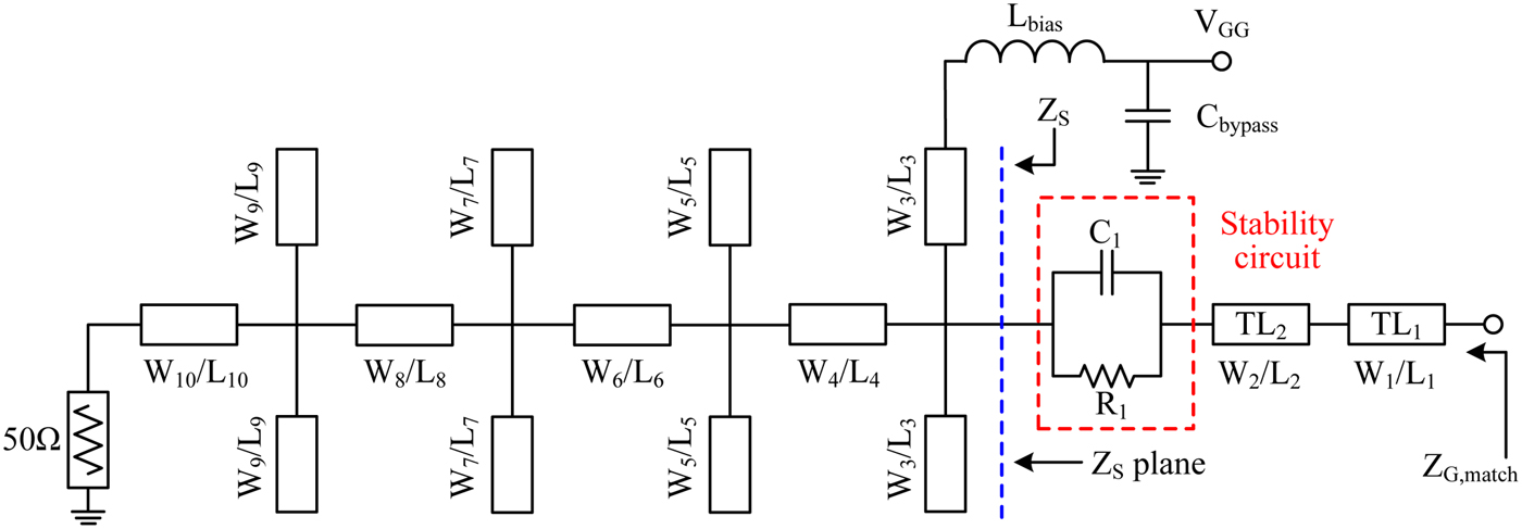
Fig. 5. Input matching network including the bias network and RC stability circuit.

Fig. 6. The optimum source impedance trajectory of CGH40010F and the source impedance Z S provided by IMN in 1.3–2.5 GHz.
Finally, an improved Chebyshev low-pass IMN is realized. The geometrical dimensions of IMN are presented in Table 1. As a figure of merit of the matching condition, the return loss S 11 of IMN at Z S plane (connected to a source load, which is the conjugate of the s1p file in step 1) and the return loss S 22 of IMN at the load (50 Ω) are plotted in Fig. 7. It is important to note that ZS provided by IMN in Fig. 6 at the edge of the operating frequency band deviates from the optimum source impedance trajectory slightly, which results in poor return loss S 11 and S 22, as shown in Fig. 7. This problem can be improved by employing higher order low-pass matching network. However, higher order low-pass matching network increases the circuit size and also the insertion loss.
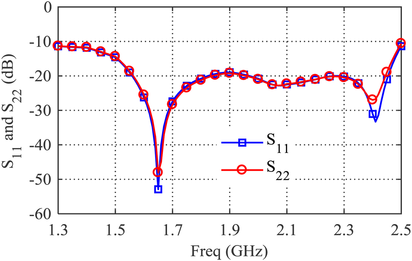
Fig. 7. The return loss S 11 and S 22 of IMN.
Table 1. Geometrical dimensions of IMN for the schematic simulation and layout EM simulation (Unit: mm)

Output matching network (OMN) design
In the same way, the proposed network is used to design the OMN, as shown in Fig. 8. For IMN in the section “Input matching network design”, we use the low-memory bias network directly, in which an inductor 27.3 nH 0908SQ-27NL is employed. As mentioned in the section “Analysis on memory effects and IMD3”, low-memory effects are achieved by minimizing the envelope voltage components and suppressing the second-harmonic output power levels. In this section, we will analyze two simple drain bias networks in detail through the bias inductors 1.3 μH 4310LC-132KE and 27.3 nH 0908SQ-27NL.

Fig. 8. OMN including a drain bias network.
The design procedure of OMN is given as follows: (1) design a real-complex lumped Chebyshev low-pass matching network within the desired bandwidth by using the method discussed in the section “Input matching network design”. (2) Insert the drain bias network into OMN with two different inductors 27.3 nH 0908SQ-27NL and 1.3 μH 4310LC-132KE, respectively. (3) Optimize lumped OMN based on the optimum load impedances while the low-envelope impedance of Z D,match is maintained. (4) Transform the lumped OMN into the distributed-OMN. (5) Post optimization is used to realize better performance due to the apparent difference between the schematic simulation and layout EM simulation. Finally, an improved Chebyshev low-pass OMN (n = 7) is obtained. To assemble the RF power transistor, the microstrip line W 1/L 1 is inserted, which is also considered in the post optimization. The geometrical dimensions of OMN are given in Table 2. The simulated results are given in Fig. 9. Although the S 21 performance of the layout circuit in the higher frequency range (5–8 GHz) is deteriorated a little bit, the excellent second-harmonic suppression can be still obtained.
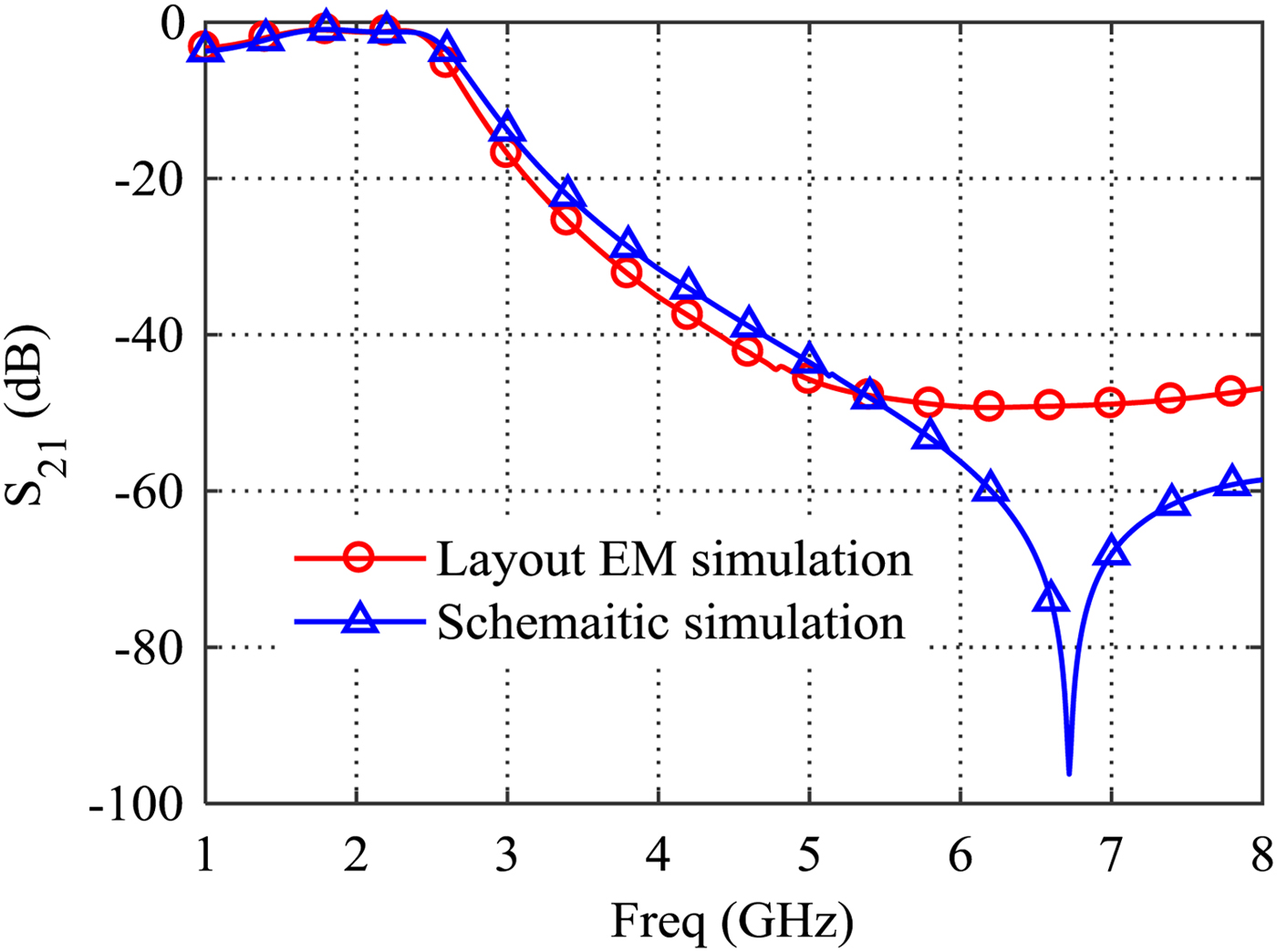
Fig. 9. Simulated S 21 of OMN with the drain bias network including an inductor 27.3 nH 0908SQ-27NL.
Table 2. Geometrical dimensions of OMN for the schematic simulation and layout EM simulation (Unit: mm)

Figure 10 shows the measured small signal gain of the fabricated wideband PA. The small signal gain in 1.35–2.45 GHz is 12.6–14.2 dB. Harmonic suppression can be observed intuitively. Table 3 shows the measured second-harmonic output power levels of the fabricated wideband PA for the drain bias network with two different bias inductors. It can be seen that the drain bias network has a fewer impact on the second-harmonic output power levels. The frequency dependent Z D,match with these two bias inductors in the low frequency range is shown in Fig. 4. Low-memory effects are realized by using the bias inductor 27.3 nH 0908SQ-27NL.
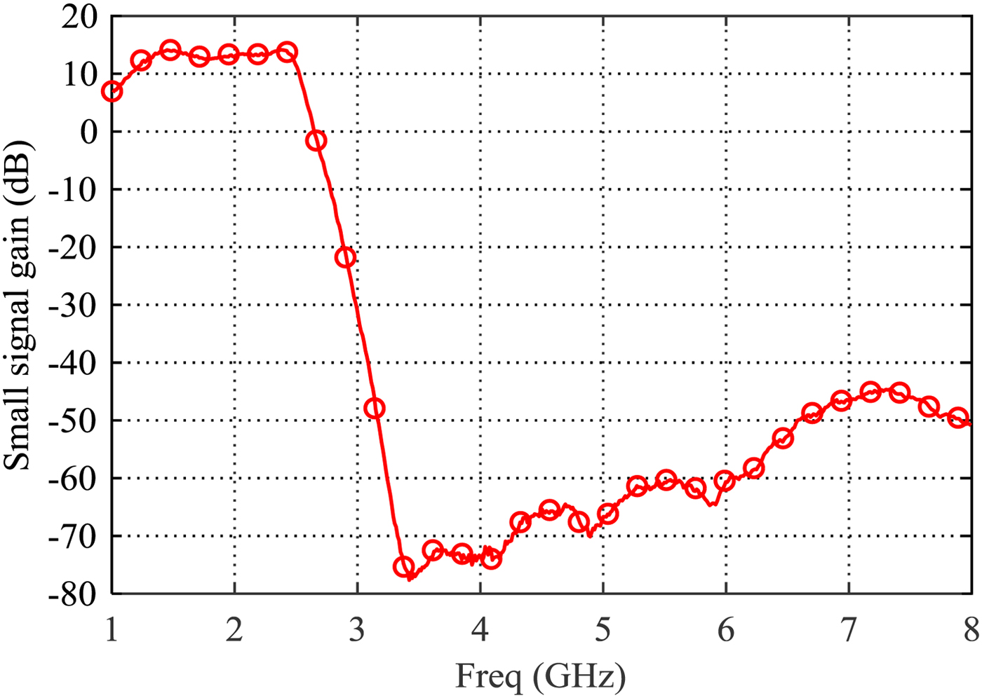
Fig. 10. Measured small signal gain of wideband PA with the drain bias network including the inductor 27.3 nH 0908SQ-27NL.
Table 3. Measured relative second-harmonic output power levels (P 2HD) of the proposed wideband PA with the output power at 1 dB compression point for two cases, relative to the fundamental output power

Note: P2HD = P 2harm − Pfund (dBc)
a Drain bias network with inductor 1.3 μH 4310LC-132KE.
b Drain bias network with inductor 27.3 nH 0908SQ-NL.
Figure 11 depicts the fundamental, second-harmonic and third harmonic load impedance Z D,match presented by the improved Chebyshev low-pass OMN. It should be noted that Z D,match is obtained by the layout EM simulation. As shown in Fig. 11, the fundamental impedances follow the optimum load impedance trajectory very well. The high-efficiency region in the dashed ellipse shows the optimum region for the second-harmonic and third harmonic impedances, which are obtained by harmonic load-pull simulation in ADS. As shown in Fig. 10, the second-harmonic and third harmonic components are suppressed by the low-pass matching network. Hence, the low second-harmonic and third harmonic output power levels are achieved. As the operating frequency increases, the low-pass matching network brings about the second-harmonic impedances at the higher frequency (>4 GHz) move out of the high-efficiency region (the dashed ellipse) and the third harmonic impedances pass through the open circuit and moves to the capacitive area along the edge of the Smith chart. The movement of the second and third harmonic impedances can result in that PAE drops to a certain extent. Despite all this, lower IMD3 is obtained and low-memory effects are achieved at the same time.

Fig. 11. Load impedance Z D,match presented by improved Chebyshev low-pass OMN with the drain bias network including an inductor 27.3 nH 0908SQ-27NL.
PA design and measured results
To validate the proposed approach, a wideband PA is designed, fabricated, and measured. The fabricated PA is shown in Fig. 12. The GaN device CGH40010F is used for implementation. A 30 mil Rogers substrate with a copper thickness of 35 μm and εr = 3.66 is selected. A stabilized circuit of a 19.9 Ω resistor and a 5.6 pF capacitor is inserted between the input matching network and RF power transistor. The RF power transistor is biased with a quiescent current of 12 mA and DC supply voltage V DD = 28 V.

Fig. 12. Photograph of the fabricated wideband PA.
Measured results with CW signal
To evaluate the high-efficiency performance, CW measurement is employed first to characterize the implemented wideband PA from 1.35 GHz to 2.45 GHz. The measured results are illustrated in Figs. 13–15. Figure 13 depicts the measured output power, drain efficiency (DE), and PAE as well as the simulated results. It can be seen that the output power is 40.0–41.2 dBm across 1.35–2.45 GHz, the PAE maintains more than 60% between 1.35 GHz and 2.45 GHz giving a fractional bandwidth of 58% and the measured DE is 66–83%. The maximum PAE of 78% and the maximum DE of 83% is measured at 1.4 GHz.

Fig. 13. Measured power gain, output power, and PAE versus frequency from 1.35 GHz to 2.45 GHz.

Fig. 14. Measured power gain versus output power at 1.4, 1.6, 1.8, 2.0, 2.2, and 2.4 GHz.

Fig. 15. Measured PAE versus output power at 1.4, 1.6, 1.8, 2.0, 2.2 and 2.4 GHz.
The measured power gain and PAE versus output power across 1.4–2.4 GHz with a frequency spacing 200 MHz are demonstrated in Figs 14 and 15. It can be seen from Fig. 14 that the 3-dB gain compression points in 1.4–2.4 GHz are 10.8–12.3 dB and the small signal gain is 14.4 ± 0.6 dB. Figure 15 illustrates that higher PAE is obtained at the lower frequency band, which is consistent with the discussion in the section “Output matching network design”.
Measured results with 20 MHz LTE modulated signal
In order to verify the capability of the fabricated wideband PA to linearly amplify wideband modulated signal, a linearization test platform was set up. This platform includes vector signal generator (NI PXIe-1075), high gain driver PA (AR-5S1G4), spectrum analyzer (R&S FSW), and PC running MATLAB software, as shown in Fig. 16. The baseband modulated signal was first loaded into NI PXIe-1075 and then up-converted to RF by NI PXIe-1075, pre-amplified by the driver AR-5S1G4, and transmitted to the proposed wideband PA. On the feedback loop, the output signal from the proposed PA was attenuated, captured, down-converted, and forwarded to the PC for DPD model training and extraction.
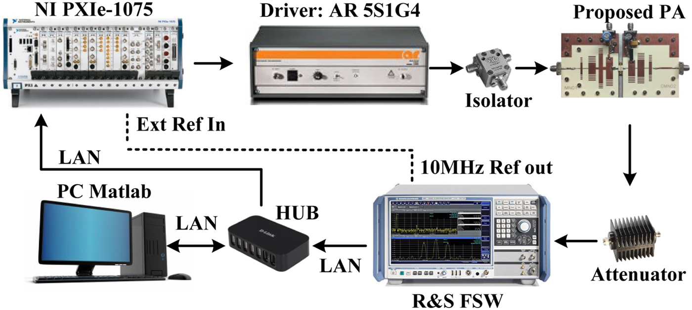
Fig. 16. Linearization test platform for 20-/40- MHz LTE modulated signal.
A 20 MHz LTE modulated signal with a peak-to-average power ratio (PAPR) of 7.6 dB was used to test the proposed wideband PA. In general, a memoryless DPD model cannot completely eliminate the memory effects, such as look-up table (LUT) model [Reference Ghannouchi and Hammi14]. Due to the proposed PA operating with wideband signals, memory effects must be taken into account by DPD model in order to fully exploit the potential of DPD [Reference Morgan, Ma, Kim, Zierdt and Pastalan15]. In the linearization measurement, the memory polynomial model with the nonlinear order 13 and memory depth 5 was used [Reference Ghannouchi, Hammi and Helaoui8]. The labels ‘Without DPD1’ and ‘With DPD1’ in Figs. 17–19 indicate that the drain bias network of the measured PA employs an inductor 1.3 μH 4310LC-132KE. The labels ‘Without DPD2’ and ‘With DPD2’ in Figs. 17–19 indicate that the drain bias network of the measured PA uses an inductor 27.3 nH 0908SQ-27NL.

Fig. 17. Measured output spectrum with and without DPD linearization for 20 MHz LTE modulated signal at (a) 1.4 GHz (b) 1.5 GHz (c) 2.0 GHz (d) 2.4 GHz.

Fig. 18. Measured ACLRs at ±20 MHz offset versus frequency from 1.4 GHz to 2.4 GHz with two different bias networks.

Fig. 19. Measured (a) phase and (b) normalized output magnitude versus normalized input magnitude at 2.14 GHz.
It can be seen from Fig. 19 that the memory effects of the fabricated wideband PA employing an inductor 1.3 μH 4310LC-132KE are significant. On the contrary, the memory effects are reduced noticeably when the drain bias network using an inductor 27.3 nH 0908SQ-27NL. Fig. 17 depicts the measured output spectrum with and without DPD linearization at an average output power of 32.4–33.6 dBm when the carrier frequencies are set at 1.4, 1.5, 2.0, and 2.4 GHz for two different drain bias networks. At these four frequencies, ACLRs at ±20 MHz offset with and without DPD are presented in Fig. 18. The strong memory effects of the measured PA employing the inductor 1.3 μH 4310LC-132KE are observed from the asymmetry of ACLRs in Figs 17 and 18. The open loop ACLRs of the measured PA employing the inductor 1.3 μH 4310LC-132KE is around −20 dBc across 1.5–2.4 GHz due to strong memory effects generated by high-envelope terminal node impedances in the megahertz range. The open loop ACLRs of the measured PA employing the inductor 27.3 nH 0908SQ-27NL is from −36 dBc to −30 dBc across 1.5–2.4 GHz, which can satisfy the requirement of DPD linearization easily. For the measured PA employing the inductor 1.3 μH 4310LC-132KE, little linearity is improved after DPD linearization. Conversely, for the low-memory wideband PA employing the inductor 27.3 nH 0908SQ-27NL, the ACLRs with DPD linearization across 1.5–2.4 GHz can be achieved around −55 dBc, and even at 1.4 GHz the ACLRs is lower than −48 dBc. The improvement on the ACLRs with DPD linearization is 19.0–25.2 dB in 1.4–2.4 GHz. It should be noted that ACLRs at ±20 MHz offset in Fig. 17(a) ‘with and without DPD2’ is relatively poor compared with Figs. 17(b) and 17(c), which is attributed to higher second-harmonic output power levels, as illustrated in Table 3. The OMN can be improved by using modified elliptic low-pass filtering network to provide a sharper roll-off [Reference Yang, Xia, Guo and Zhu16].
Measured results with 40 MHz two-carrier LTE modulated signal
Due to NI 5973 RF transmitter adapter module of vector signal generator (NI PXIe-1075) only has a 200 MHz bandwidth, 40 MHz two-carrier LTE modulated signal with a PAPR of 10.4 dB is adopted to further verify the performance of the implemented PA with DPD linearization. As discussed inthe section “Measured results with 20 MHz LTE modulated signal”, the implemented PA employing the inductor 1.3 μH 4310LC-132KE has strong memory effects. Hence, only the proposed PA employing the inductor 27.3 nH 0908SQ-27NL is linearized with the same DPD linearization method of the section “Measured results with 20 MHz LTE modulated signal” at an average output power of ~30.5 dBm from 1.5 GHz to 2.4 GHz, as shown in Fig. 20. The measured ACLRs at ±40 MHz offset are displayed in Fig. 21 and the average drain efficiency is presented in Table 5.

Fig. 20. Measured output spectrum with and without DPD linearization for 40 MHz two-carrier LTE modulated signal at (a) 1.5 GHz (b) 1.8 GHz (c) 2.1 GHz (d) 2.4 GHz.
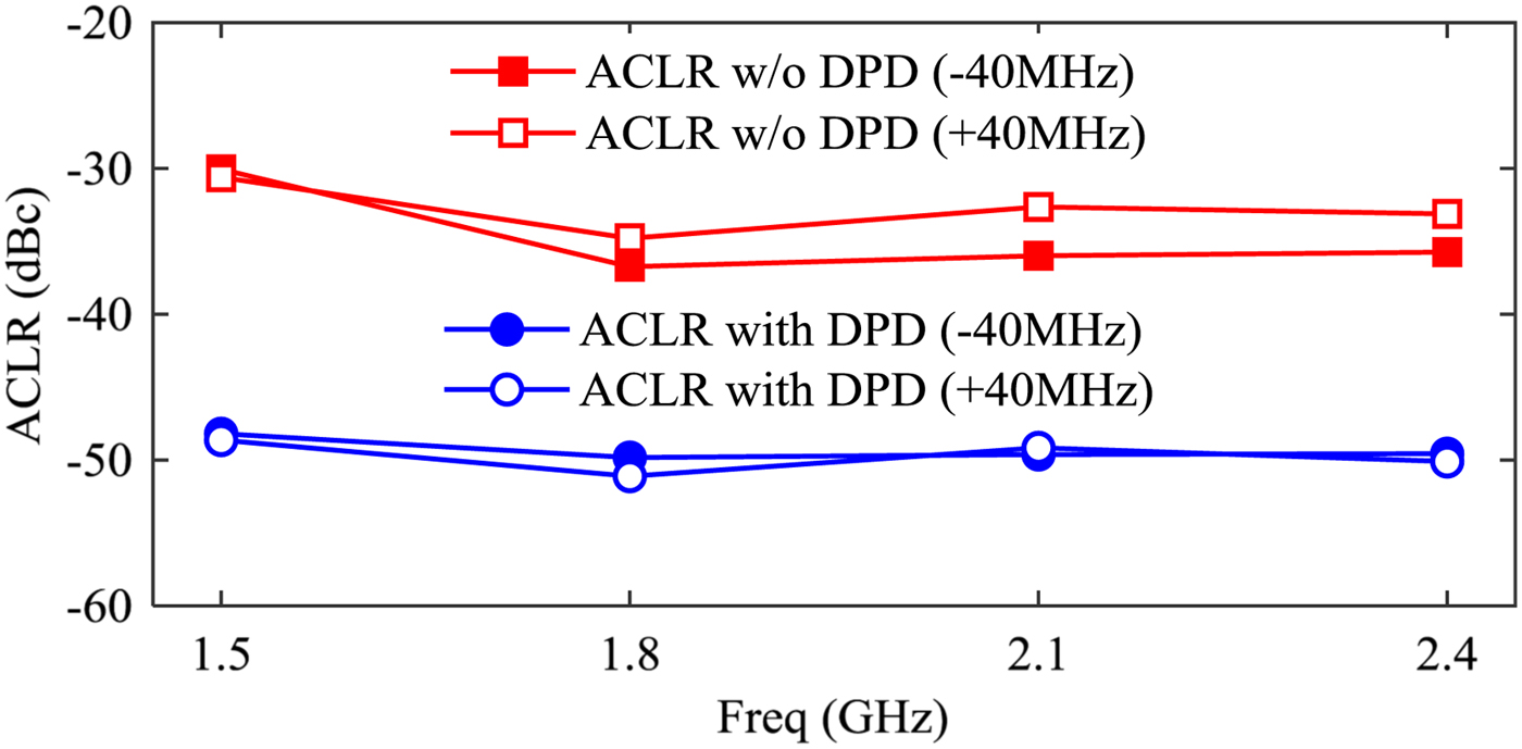
Fig. 21. Measured ACLRs at ±40 MHz offset versus frequency from 1.5 GHz to 2.4 GHz.
Wideband PAs performance comparison
The proposed PA is compared with other reported wideband PAs, as shown in Tables 4 and 5. In [Reference Saad, Fager, Cao, Zirath and Andersson1, Reference Ding, He, You, Xie and Hu2, Reference Tuffy, Guan, Zhu and Brazil5], the reported wideband PAs exhibit wider operating band, but their DE is relatively lower compared with the proposed PA, as shown in Table 4. Meanwhile, their linearization test was done only at a single frequency, and the test results indicate relatively poor performance compared with the proposed PA, as illustrated in Table 5. Compared with [Reference Yang, Xia, Guo and Zhu16], although the proposed PA has the similar RF performance under CW measurement, Table 5 indicates that the proposed PA in this work shows better linearization performance. The ACLRs with DPD linearization for 20 MHz LTE signal at ±20 MHz offset are −55.7 ~ −53.9 dBc and the ACLRs with DPD linearization for 40 MHz LTE signal at ±40 MHz offset are −51.1 ~ −48.2 dBc in the frequency range from 1.5 GHz to 2.4 GHz. The excellent linearity of the proposed PA can be mainly attributed to the reduction in memory effects and IMD3.
Table 4. Wideband PAs performance comparison with CW signals

a CGH60015D is used as the RF power transistor.
b CGH40010F is used as the RF power transistor.
Table 5. Wideband PAs performance comparison with modulated signals

PAPR, peak-to-average power ratio.
BW, bandwidth AE, average drain efficiency.
a Only DPD linearization at a single frequency is given in [Reference Saad, Fager, Cao, Zirath and Andersson1, Reference Ding, He, You, Xie and Hu2, Reference Tuffy, Guan, Zhu and Brazil5].
Conclusion
An analytical method is proposed and analyzed in this work to reduce the memory effects and IMD3. The improved low-pass matching network can restrain the second-harmonic output power levels and reduce IMD3. At the same time, it provides low-envelope impedances for the terminal nodes in the megahertz range, which can reduce the envelope voltage components and lead to low-memory effects. After DPD linearization, the proposed PA driven with two LTE modulated signals shows excellent ACLR specification of −55.7 ~ −53.9 dBc at ±20 MHz offset (20 MHz LTE signal) and −51.1 ~ −48.2 dBc at ±40 MHz offset (40 MHz two-carrier LTE signal) across 1.5–2.4 GHz. Although two simple drain bias networks are used to validate the proposed method, the work carried out in this paper, can give a clear idea to design wideband high-efficiency PA when high linearity is indispensable or which is needed to be compatible with DPD linearization technique friendly.
Acknowledgments
This work was supported by National Nature Science Foundation of China (Grant 61501090), Open Foundation of State Key Laboratory of Millimeter Waves (Grant K201604), China Scholarship Council, Alberta Innovates Technology Futures (AITF), National Science and Engineering Research Council (NSERC) of Canada, and Canada Research Chairs (CRC) Program. The authors would like to thank Cree Inc., for providing the large-signal transistor model of GaN device CGH40010F, Modelithics Inc., for providing the model library of Coilcraft inductors, and Coilcraft Inc., for providing the inductor samples.
 Xuekun Du received the M.Sc. degree in communication and information system from Liaoning Technical University, Huludao, China, in 2014. He is currently pursuing the Ph.D. degree in communication and information system at the University of Electronic Science and Technology of China, Chengdu, China. Since 2016, he has been a Visiting Ph.D. Student with the Intelligent RF Radio Laboratory (iRadio Lab), Department of Electrical and Computer Engineering, University of Calgary, Calgary, AB, Canada. His current research interests include passive circuit design, high efficient wideband power amplifier design, and monolithic microwave integrated circuit (MMIC) modeling and power amplifier design.
 Chang Jiang You received the B.S. degrees from University of Electronic Science and Technology of China and the Ph.D. degrees from Southeast University, in 2006 and 2012 respectively. From April 2011 to October 2011, he was a Researcher with the Institute for Infocomm Research, A*STAR, Singapore. From October 2015 to October 2016, he has been a visiting scholar with National University of Singapore. Since 2012, he has been with University of Electronic Science and Technology of China, Chengdu, China, where he is currently an Associate Professor with the School of Communication and Information Engineering. His research interests include power amplifier, filter and antenna technologies for wireless communications, as well as microwave & millimeter-wave theory and technology. He has authored or co-authored over 60 technical papers.
 Yulong Zhao received the B.S. degree in applied physics and M.S. degree in electronic engineering from Xidian University, Xi'an, China, in 2006 and 2009. He is currently working toward the Ph.D. degree at the University of Calgary, Calgary, AB, Canada. From 2009 to 2015, he was a Microwave Engineer and Project Leader with ZTE Corporation. He was with the Radio Remote Unit development department, where he designed high-power amplifiers for 3G and 4G wireless communications. He is currently with the Intelligent RF Radio Technology Laboratory (iRadio Lab), University of Calgary. His research interests include high efficiency and wideband RF PAs, MMIC PAs, and microwave passive components.
 Xiang Li received the B.Sc. and M.Sc. degrees in Electronic Engineering from Tsinghua University, Beijing, China, in 2009 and 2012, respectively. He is currently working towards the Ph.D. degree at University of Calgary, Calgary, AB, Canada. His research interests include multi-band/wide-band power amplifier design, outphasing transmitter design and MMIC power amplifiers for wireless and satellite communication. Mr. Li was the recipient of the Student Paper Award of 2010 Asia-Pacific Microwave Conference (APMC). He was also the recipient of Alberta Innovates-Technology Futures (AITF) Award and Eyes High International Doctoral Scholarship at the University of Calgary in 2016.
 Mohamed Helaoui received the M.Sc. degree in communications and information technology from ’Ecole Supérieure des Communications de Tunis, Ariana, Tunisia, in 2003, and the Ph.D. degree in electrical engineering from the University of Calgary, Calgary, AB, Canada, in 2008. He is currently an Associate Professor with the Department of Electrical and Computer Engineering, University of Calgary. He has authored or co-authored over 130 publications, 1 book, and 3 book chapters. He holds seven patents with four pending. His current research interests include digital signal processing, power efficiency enhancement for wireless transmitters, switching-mode power amplifiers, six-port receivers, and advanced transceiver design for software defined radio and millimeter-wave applications.
 Jingye Cai received the B.Sc. degree in Radio-Electronic Engineering from Sichuan University, Chengdu, China, in 1983 and the M.Sc. degree in Signal and Information Processing Engineering from University of Electronic Science and Technology of China (UESTC), Chengdu, China, in 1990. He is currently a Professor, Director of Digital Information Processing Laboratory and Associate Dean of the School of Information and Software Engineering, UESTC. His research interests are in the areas of signal processing in modern communication (Radar), frequency synthesis technique, RF circuits & systems in electronic systems and phase noise measurement & spectrum estimation technique. He has hosted and actualized more than 20 research projects, in which he has won the second prize of national defense science and technology achievement on small-size full-phase-coherence millimeter-wave frequency synthesizer and other seven achievement awards.
 Fadhel M. Ghannouchi is currently a Professor, Alberta Innovates/the Canada Research Chair, and the Founding Director of the iRadio Laboratory, Department of Electrical and Computer Engineering, University of Calgary, Calgary, AB, Canada. He held several invited positions at several academic and research institutions in Europe, North America, and Japan. He has provided consulting services to a number of microwave and wireless communications companies. He has authored or co-authored over 650 publications. He holds 16 U.S. patents with four pending. His current research interests include microwave instrumentation and measurements, nonlinear modeling of microwave devices and communications systems, design of power- and spectrum-efficient microwave amplification systems, and design of intelligent RF transceivers for wireless and satellite communications.


