


I. INTRODUCTION
Radomes are important components of antenna systems because they are sheltering structures to protect antennas against severe weather such as high winds, rain, icing, and/or temperature extremes [Reference Skolnik1]. On the other hand, Radomes must not interfere with normal operation of the antennas and so the input reflection of Radomes must be negligible at the usable frequency band of the protected antennas. So far, several structures have been introduced as Radomes such as single dielectric layer [Reference Chang and Chan2–Reference Crone, Rudge, Mem and Taylor6], multilayer dielectric slab [Reference Crone, Rudge, Mem and Taylor6–Reference Paris8], metal space frame [Reference Kay9–Reference Altintas, Ouardani and Yurchenko11], grooved dielectric layer [Reference Bodnar and Bassett12], streamlined metallic [Reference Pelton and Munk13], and inhomogeneous planar layer [Reference Khalaj-Amirhosseini14]. In this paper, we propose a new structure to operate as wideband and wide-angle flat Radome. In this structure several dielectric and ferrite layers are alternately located beside each other to behave as a single matched slow wave layer. First, the relationship between the permittivity and permeability of a required fictitious mixed material is obtained. Then the required permittivity and permeability of dielectric and ferrite layers are obtained at desired incidence angle. The performance of the proposed structure is investigated and validated using some theoretical and simulation examples.
II. RADOMES DESIGN
In this section, the idea to design wideband Radomes using dielectric and ferrite layers is presented. Figure 1(a) shows the cross section of a flat Radome of thickness d composed of a fictitious mixed material of permittivity ɛ rm and of permeability μ rm, called mixed material Radome (MMR). There have been quite a few patents based on this structure by composite materials [15, 16]. Also, Fig. 1(b) shows the cross section of a flat Radome of thickness d consisting of N cascaded basic structures, i.e. a ferrite (μ r) layer between two dielectric (ɛ r) layers. We call this Radome as dielectric ferrite Radome (DFR), which is consisting of 2N + 1 successive dielectric and ferrite layers. It is proved in the next section that the performance of the DFRs can be an approximation of that of MMRs. The thickness Δz in Fig. 1(b) is given by
 $$\Delta z = \displaystyle{d \over 2N}.$$
Fig. 1. (a) The cross section of a flat Radome of thickness d composed of a fictitious mixed material (MMR). (b) The cross section of a flat Radome of thickness d consisting of 2N + 1 dielectric and ferrite layers alternately (DFR).
It is assumed that the incidence plane wave propagates in the free space obliquely with an angle of incidence θ i. Also, two different polarizations are possible, one is the TM and the other is the TE. Of course, we know that the wave radiated by an antenna can be decomposed into many plane waves with different incidence angles. We would like to design the structures shown in Fig. 1 as Radomes in a wide incidence angle and at a wide frequency range. To analyze and design the proposed structures, the undesirable phenomena such as losses, frequency dispersion, and surface waves have not taken into account.
A) MMR design
The chain parameter matrix of the equivalent layer is given by [Reference Balanis17]
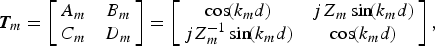 $${\bi T}_m = \left[\matrix{A_m &B_m \cr C_m &D_m} \right]= \left[\matrix{\cos \!\lpar k_m d\rpar & jZ_m \sin \!\lpar k_m d\rpar \cr jZ_m^{ - 1} \sin \!\lpar k_m d\rpar & \cos \!\lpar k_m d\rpar } \right]\comma \;$$
where k m and Z m are the propagation coefficient and the characteristic impedance of the MMR, respectively, given by
 $$k_m = k_0 \sqrt{\mu_{rm} \varepsilon_{rm} - \sin ^2 \lpar \theta _i \rpar }\comma \;$$
 $$Z_m = \left\{\matrix{\displaystyle{\eta_0 \mu_{rm} \over \sqrt{\mu_{rm} \varepsilon_{rm} - \sin^2 \lpar \theta_i\rpar }}\comma \; &TE\comma \; \cr \displaystyle{\eta_0 \over \varepsilon_{rm}} \sqrt{\mu_{rm} \varepsilon_{rm} - \sin^2 \lpar \theta_i\rpar }\comma \; &TM\comma \; } \right.$$
in which k 0 = 2πf/c (c is the velocity of the light) and η 0 are the wave number and the impedance wave, respectively, in the free space. The reflection coefficients from two surfaces of the MMRs are given by [Reference Balanis17]
 $$\Gamma_{TE} = {\mu_{rm} \cos \!\lpar \theta_i \rpar - \sqrt{\mu_{rm} \varepsilon_{rm} - \sin^2 \lpar \theta_i\rpar } \over \mu_{rm} \cos \!\lpar \theta_i\rpar + \sqrt{\mu_{rm} \varepsilon_{rm} - \sin^2 \lpar \theta _i\rpar }}\comma \;$$
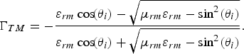 $$\Gamma_{TM} = - {\varepsilon_{rm} \cos \!\lpar \theta_i \rpar - \sqrt{\mu_{rm} \varepsilon_{rm} - \sin^2 \lpar \theta_i\rpar } \over \varepsilon _{rm} \cos \!\lpar \theta_i\rpar + \sqrt{\mu_{rm} \varepsilon_{rm} - \sin^2 \lpar \theta_i\rpar }}.$$
To have no reflection at desired incidence angle θ i = θ 0 (similar to Brewster's angle), one of the following relations has to be held according to (5) and (6):
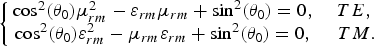 $$\left\{\matrix{\cos^2 \lpar \theta_0\rpar \mu_{rm}^2 - \varepsilon_{rm} \mu_{rm} + \sin^2 \lpar \theta_0\rpar = 0\comma \; & TE\comma \; \cr \cos^2 \lpar \theta_0\rpar \varepsilon_{rm}^2 - \mu_{rm} \varepsilon_{rm} + \sin^2 \lpar \theta_0\rpar = 0\comma \; &TM. } \right.$$
The relations in (7) translate the fact that the characteristic impedance of the MMR in (4) should be equal to that of free space, in order that the matching condition be satisfied. From (7), the relationship between the permittivity and permeability of the mixed material has to be as follows:
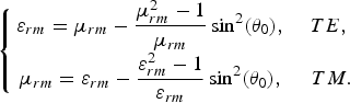 $$\left\{\matrix{\displaystyle\varepsilon_{rm} = \mu_{rm} - {\mu_{rm}^2 - 1 \over \mu_{rm}} \sin^2 \lpar \theta_0\rpar \comma \; &TE\comma \; \cr \displaystyle\mu_{rm} = \varepsilon_{rm} - {\varepsilon_{rm}^2 - 1 \over \varepsilon_{rm}} \sin^2 \lpar \theta_0\rpar \comma \; &TM.} \right.$$
It is seen that the required permittivity or permeability is dependent on the desired incidence angle. Here, we are looking for simultaneous validation of (8) for both TE and TM waves. In a special case of θ 0 = 0°, which is the practical case for Radomes, the required permittivity and permeability must be equal to each other, i.e. ɛ rm = μ rm, which gives a characteristic impedance equal to η 0 at θ i = 0°. In this case, the magnitude of TE and TM reflection coefficients becomes the same for all incidence angles as deduced from (5) and (6). Finally, substituting (8) in (5) and (6) yields us the following relations for the reflection coefficients of the surfaces, which are zero at θ i = θ 0:
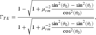 $$\Gamma_{TE} = {1 - \sqrt{\displaystyle1 + \mu_{rm}^{ - 2} {\sin^2 \lpar \theta_0\rpar - \sin^2 \lpar \theta_i\rpar \over \cos^2 \lpar \theta_0\rpar }} \over 1 + \sqrt{\displaystyle1 + \mu_{rm}^{ - 2} {\sin^2 \lpar \theta_0\rpar - \sin^2 \lpar \theta_i\rpar \over \cos^2 \lpar \theta_0\rpar }}}\comma \;$$
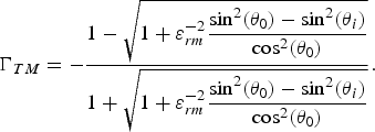 $$\Gamma_{TM} = - {1 - \sqrt{\displaystyle1 + \varepsilon_{rm}^{ - 2} {\sin^2 \lpar \theta_0\rpar - \sin^2 \lpar \theta_i\rpar \over \cos^2 \lpar \theta_0\rpar }} \over 1 + \sqrt{\displaystyle1 + \varepsilon_{rm}^{ - 2} {\sin^2 \lpar \theta _0 \rpar - \sin \!^2 \lpar \theta _i\rpar \over \cos^2 \lpar \theta_0 \rpar }}}.$$
B) DFR design
The construction of desired MMR materials is actually not practical. So, we approximate them by cascading N basic DFR structures as shown in Fig. 1(b). The chain parameter matrix of the whole DFR can be written as follows:
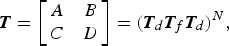 $${\bi T} = \left[\matrix{A & B \cr C & D} \right]= \lpar {\bi T}_d {\bi T}_f {\bi T}_d\rpar ^N\comma \;$$
in which Td and Tf are the chain parameter matrices of the dielectric and ferrite layers, respectively, as follows:
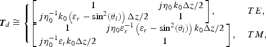
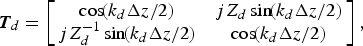 $${\bi T}_d = \left[\matrix{\cos \!\lpar k_d \Delta z/2\rpar &jZ_d \sin \!\lpar k_d \Delta z/2\rpar \cr jZ_d^{ - 1} \sin \!\lpar k_d \Delta z/2\rpar &\cos \!\lpar k_d \Delta z/2\rpar } \right]\comma \;$$
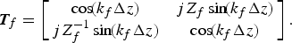 $${\bi T}_f = \left[\matrix{\cos \!\lpar k_f \Delta z\rpar &jZ_f \sin \!\lpar k_f \Delta z\rpar \cr jZ_f^{ - 1} \sin \!\lpar k_f \Delta z\rpar &\cos \!\lpar k_f \Delta z\rpar } \right].$$
In (12) and (13), the propagation coefficients and the characteristic impedances are as follows:
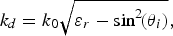 $$k_d = k_0 \sqrt{\varepsilon_r - \sin ^2 \!\lpar \theta _i \rpar }\comma \;$$
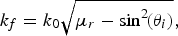 $$k_f = k_0 \sqrt{\mu _r - \sin ^2 \!\lpar \theta_i\rpar }\comma \;$$
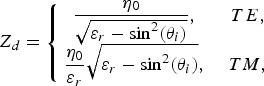 $$Z_d = \left\{\matrix{\displaystyle{\eta_0 \over \sqrt{\varepsilon_r - \sin^2 \lpar \theta_i\rpar }}\comma \; &TE\comma \; \cr \displaystyle{\eta_0 \over \varepsilon_r} \sqrt{\varepsilon_r - \sin^2 \lpar \theta_i\rpar }\comma \; &TM\comma \; } \right.$$
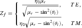 $$Z_f = \left\{\matrix{\displaystyle{\eta_0 \mu_r \over \sqrt{\mu_r - \sin^2 \lpar \theta_i\rpar }}\comma \; &TE\comma \; \cr \displaystyle \eta_0 \sqrt{\mu_r - \sin^2 \lpar \theta_i\rpar }\comma \; &TM.} \right.$$
The chain parameter matrices of dielectric and ferrite layers assuming Δz ≪ λ 0, where λ 0 is the wavelength in free space, can be approximated by
 $${\bi T}_d \cong \left\{\matrix{\left[\matrix{1 &j\eta_0\, k_0 \Delta z/2 \cr j\eta_0^{ - 1} k_0 \left(\varepsilon_r - \sin^2 \lpar \theta_i \rpar \right)\Delta z/2 &1} \right]\comma \; \hfill &TE\comma \; \hfill \cr \left[\matrix{1 & j\eta_0 \varepsilon _r^{ - 1} \left(\varepsilon_r - \sin^2 \lpar \theta_i\rpar \right)k_0 \Delta z/2 \cr j\eta_0^{ - 1} \varepsilon_r k_0 \Delta z/2 & 1} \right]\comma \; \hfill &TM\comma \; } \right.$$
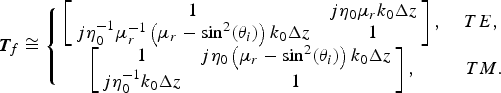 $${\bi T}_f \cong \left\{\matrix{\left[\matrix{1 & j\eta_0 \mu_r k_0 \Delta z \hfill \cr j\eta_0^{ - 1} \mu_r^{ - 1} \left(\mu_r - \sin^2 \lpar \theta_i\rpar \right)k_0 \Delta z \hfill & 1} \right]\comma \; & TE\comma \; \cr \left[\matrix{1 & j\eta_0 \left(\mu_r - \sin^2 \lpar \theta_i\rpar \right)k_0 \Delta z \cr j\eta_0^{ - 1} k_0 \Delta z & 1} \right]\comma \; & TM.} \right.$$
Therefore, the chain parameter matrix of a DFR with thickness 2Δz ≪ λ 0, can be approximated by
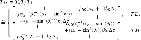 $$\eqalign{&{\bi T}_{df} = {\bi T}_d {\bi T}_f {\bi T}_d \cr &\cong \left\{\matrix{\left[\matrix{1 & j\eta_0 \lpar \mu_r + 1\rpar k_0 \Delta z \cr \matrix{j\eta_0^{ - 1} \lpar \mu_r^{ - 1} \lpar \mu_r - \sin^2 \lpar \theta_i\rpar \rpar \cr + \lpar \varepsilon_r - \sin^2 \lpar \theta _i\rpar \rpar \rpar k_0 \Delta z} & 1} \right]\comma \; \hfill &TE\comma \; \cr \left[\matrix{1 &\matrix{j\eta_0 \lpar \varepsilon_r^{ - 1} \lpar \varepsilon_r - \sin^2 \lpar \theta_i\rpar \rpar \cr + \lpar \mu_r - \sin^2 \lpar \theta_i\rpar \rpar \rpar k_0 \Delta z} \cr j\eta _0^{ - 1} \left(\varepsilon_r + 1 \right)k_0 \Delta z & 1} \right]\comma \; \hfill &TM.} \right.}$$
On the other hand, the chain parameter matrix of the MMR (2) with thickness 2Δz ≪ λ 0, can be approximated by
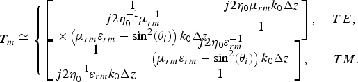 $${\bi T}_m \cong \left\{\matrix{\left[\matrix{1 &j2\eta _0 \mu_{rm} k_0 \Delta z \cr \matrix{j2\eta_0^{ - 1} \mu_{rm}^{ - 1} \cr \times\left(\mu_{rm} \varepsilon_{rm} - \sin ^2 \lpar \theta_i\rpar \right)k_0 \Delta z} & 1} \right]\comma \; \hfill &TE\comma \; \cr \left[\matrix{1 &\matrix{j2\eta_0 \varepsilon_{rm}^{ - 1} \cr \left(\mu_{rm} \varepsilon_{rm} - \sin ^2 \lpar \theta_i \rpar \right)k_0 \Delta z} \cr j2\eta _0^{ - 1} \varepsilon_{rm} k_0 \Delta z \hfill & 1} \right]\comma \; \hfill &TM.} \right.$$
Comparing (20) with (21), the following relationships are obtained between the permittivity and permeability of MMRs and those of DFRs for TE and TM polarizations, respectively:
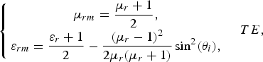 $$\left\{\matrix{\displaystyle\mu_{rm} = {\mu_r + 1 \over 2}\comma \; \cr \displaystyle \varepsilon_{rm} = {\varepsilon_r + 1 \over 2} - {\lpar \mu _r - 1\rpar ^2 \over 2\mu_r \lpar \mu_r + 1\rpar } \sin^2 \lpar \theta_i\rpar \comma \; } \quad TE\comma \; \right.$$
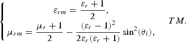 $$\left\{\matrix{\displaystyle\varepsilon_{rm} = {\varepsilon_r + 1 \over 2}\comma \; \cr \displaystyle\mu_{rm} = {\mu_r + 1 \over 2} - {\lpar \varepsilon_r - 1\rpar ^2 \over 2\varepsilon_r \lpar \varepsilon_r + 1\rpar } \sin^2 \lpar \theta_i\rpar \comma \; } \quad TM. \right.$$
It is seen that the equivalent permittivity or permeability varies with respect to the incidence angle, respectively, for TE and TM polarizations. At normal incidence, θ i = 0, the equivalent permittivity and permeability are the same for both TE and TM polarizations. Also, it is interesting to note that the equivalent permittivity and permeability are, respectively, the average of permittivities and permeabilities of the layers, at normal incidence, i.e. ɛ rm = (ɛ r + 1)/2 and μ rm = (μ r + 1)/2.
The above discussion leads us to design of DFRs. We choose either the permittivity or the permeability of the required mixed material and then use (8) to obtain the other one. Then, the required permittivity and permeability of dielectric and ferrite layers can be obtained from (22) or (23) at desired incidence angle. Of course, we have to actually choose the required permittivity and permeability of dielectric and ferrite layers equal to each other because θ 0 is near to zero in Radomes.
Moreover, the chain parameter matrix of a DFR (11) can be used to find its reflection and transmission coefficients, as follows:
 $$\Gamma = {\lpar A - Z_0 C\rpar Z_0 + \lpar B - Z_0 D\rpar \over \lpar A + Z_0 C\rpar Z_0 + \lpar B + Z_0 D\rpar }\comma \;$$
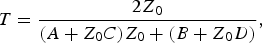 $$T = {2Z_0 \over \lpar A + Z_0 C\rpar Z_0 + \lpar B + Z_0 D\rpar }\comma \;$$
where Z 0 is the transverse characteristic impedance of the free space given by
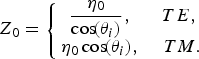 $$Z_0 = \left\{\matrix{\displaystyle{\eta_0 \over \cos \!\lpar \theta_i\rpar }\comma \; &TE\comma \; \cr \eta_0 \cos \!\lpar \theta_i\rpar \comma \; &TM.} \right.$$
III. UNDESIRABLE PHENOMENA
In the proposed Radomes such as the conventional ones, there are some undesirable phenomena such as insertion phase delay, surface waves, losses, frequency dispersion and variation by temperature and power. In this section, two undesirable phenomena of insertion phase delay and surface waves are studied. It is assumed that ɛ rm = μ rm = (ɛ r + 1)/2 = (μ r + 1)/2 for MMRs and DFRs to keep θ 0 = 0 according to (8), (22), and (23).
A) Non-ideal ferrites
In the proposed structure the ferrite layers have been considered lossless and of permittivity equal to 1. However, in practice, the permittivity of ferrites may be greater than one along with they are lossy. In both cases, the discussion above the proposed structure could be still justifiable as shown below.
If the permittivity of ferrite layers is considered as ɛrf ≠ 1, then one can obtain the following relations instead of (22) and (23):
 $$\left\{\matrix{\displaystyle\mu_{rm} = {\mu_r + 1 \over 2}\comma \; \cr \varepsilon_{rm} = \displaystyle{\varepsilon_r + \varepsilon_{rf} \over 2} - {\lpar \mu _r - 1\rpar ^2 \over 2\mu_r \lpar \mu_r + 1\rpar } \sin^2 \lpar \theta_i\rpar \comma \; } \quad TE \right.\comma \;$$
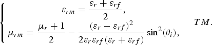 $$\left\{\matrix{\displaystyle\varepsilon_{rm} = {\varepsilon_r + \varepsilon_{rf} \over 2}\comma \; \cr \displaystyle\mu_{rm} = {\mu_r + 1 \over 2} - {\lpar \varepsilon_r - \varepsilon_{rf}\rpar ^2 \over 2\varepsilon_r \varepsilon_{rf} \lpar \varepsilon_r + \varepsilon_{rf}\rpar } \sin^2 \lpar \theta_i\rpar \comma \; } \quad TM. \right.$$
Again, the equivalent permittivity and permeability are, respectively, the average of permittivities and permeabilities of the layers, at normal incidence.
Now, if the ferrite layers have an attenuation factor equal to  $\alpha _f \ne 0$, their chain parameter matrices are modified from (13) to the following one:
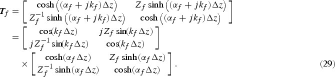 $$\eqalignno{{\bi T}_f & =\left[\matrix{\cosh \left(\lpar \alpha_f + jk_f\rpar \Delta z \right)&Z_f \sinh \left(\lpar \alpha_f + jk_f\rpar \Delta z \right)\cr Z_f^{ - 1} \sinh \left(\lpar \alpha_f + jk_f\rpar \Delta z \right)&\cosh \left(\lpar \alpha_f + jk_f\rpar \Delta z \right)} \right]\cr & =\left[\matrix{\cos \!\lpar k_f \Delta z\rpar &jZ_f \sin \!\lpar k_f \Delta z\rpar \cr jZ_f^{ - 1} \sin \!\lpar k_f \Delta z\rpar &\cos \!\lpar k_f \Delta z\rpar } \right]\cr &\quad \times \left[\matrix{\cosh \lpar \alpha_f \Delta z\rpar &Z_f \sinh \lpar \alpha_f \Delta z\rpar \cr Z_f^{ - 1} \sinh \lpar \alpha_f \Delta z\rpar &\cosh \lpar \alpha_f \Delta z\rpar } \right]. & \lpar 29\rpar}$$
It is seen that the chain matrix of a lossy ferrite layer is a multiplication of that of lossless ferrite layer by a matrix that indicates the insertion loss of the layer. So, the loss of ferrite and also dielectric layers can be extracted from the calculations and be considered as insertion loss.
B) Insertion phase delay
Ignoring Radome wall interface reflection effects, the insertion time delay (the difference between time delay of Radome and free space of the same thickness) can be expressed as follows for conventional dielectric Radomes, MMRs, and DFRs, respectively:
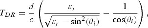 $$T_{DR} = {d \over c} \left({\varepsilon_r \over \sqrt{\varepsilon_r - \sin^2 \lpar \theta_i\rpar }} - {1 \over \cos \!\lpar \theta_i\rpar } \right)\comma \;$$
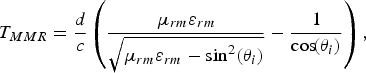 $$T_{MMR} = {d \over c} \left({\mu_{rm} \varepsilon_{rm} \over \sqrt{\mu_{rm} \varepsilon_{rm} - \sin^2 \lpar \theta_i\rpar }} - {1 \over \cos \!\lpar \theta_i\rpar } \right)\comma \;$$
 $$T_{DFR} \cong T_{MMR} = {d \over c} \left({\lpar \varepsilon_r + 1\rpar ^2 \over 2\sqrt{\lpar \varepsilon_r + 1\rpar ^2 - 4\sin^2 \lpar \theta_i\rpar }} - {1 \over \cos \!\lpar \theta_i\rpar } \right).$$
As seen from (30) to (32), it results that T MMR ≥ T DFR > T DR for the same thickness and permittivity.
C) Surface waves
From [Reference Balanis17], the surface waves of a magneto-dielectric slab (MMR) have the following cut-off frequencies:
 $$f_c = {nc \over 2d\sqrt{\varepsilon_{rm}^2 - 1}}\comma \;$$
where n = 0, 1, 2, … for TM n and TE n modes. Also, one can determine the phase constant (β) of dominant modes TM 0 and TE 0 along the surface of the Radomes from the following relationship:
 $$\tan \left(k_0 {d \over 2} \sqrt{\varepsilon_{rm}^2 - \lpar \beta /k_0 \rpar ^2} \right)= \varepsilon_{rm} \sqrt{{\lpar \beta /k_0 \rpar ^2 - 1 \over \varepsilon_{rm}^2 - \lpar \beta /k_0\rpar ^2}}.$$
After finding out β from (34), the attenuation factor of surface waves perpendicular to the Radome surface can be obtained as follows:
 $$\alpha = \sqrt{\beta^2 - k_0^2}.$$
For DFRs, (33)–(35) can be approximately used through substituting (ɛ r + 1)/2 for ɛ rm.
IV. EXAMPLES AND RESULTS
In this section the operation of the proposed structure, DFR, as a wideband and wide-angle Radome is validated using some examples. Figures 2–4 illustrate the magnitude of TE and TM reflection coefficients of DFR and MMR at frequency f = 10 GHz versus μ r and ɛ r, d and θ i, respectively, considering N = 1, 2, 3, and 4 cascaded basic structures. The assumptions of Figs 2–4 are (d = 5 mm and θ i = θ 0 = 0°), (μ r = ɛ r = 2 and θ i = θ 0 = 0°), and (μ r = ɛ r = 2, θ 0 = 0° and d = 5 mm). The nulls appeared in Figs 2 and 3 are due to the fact that DFR acts almost as an MMR when its thickness is a half of the wavelength (inside DFR). Also, Figs 5 and 6 illustrate the magnitude of TE and TM reflection coefficients of DFR and MMR of thickness d = 5 mm at frequency f = 10 GHz versus θ i assuming θ 0 = 45° for TE and TM polarizations. Assuming θ 0 = 45° for TE polarization requires μ r = 2, ɛ r = 1.25, μ rm = 1.5, and ɛ rm = 1.083 and that for TM polarization requires μ r = 1.25, ɛ r = 2, μ rm = 1.083, and ɛ rm = 1.5. From Figs 2–6 the accuracy of design relations (8), (22), and (23) is verified and it is seen that as the number of cascaded basic structures is increased the performances of DFRs approach those of MMRs which has no reflection at θ i = θ 0.

Fig. 2. The |ΓTE| and |ΓTM| of DFR at f = 10 GHz versus μ r and ɛ r, assuming d = 5 mm and θ i = θ 0 = 0° (those of MMR are minus infinite).

Fig. 3. The |ΓTE| and |ΓTM| of DFR at f = 10 GHz versus d, assuming μ r = ɛ r = 2 and θ i = θ 0 = 0° (those of MMR are minus infinite).

Fig. 4. The |ΓTE| and |ΓTM| of DFR and MMR at f = 10 GHz versus θ i, assuming d = 5 mm and μ r = ɛ r = 2 (θ 0 = 0°).

Fig. 5. The |ΓTE| and |ΓTM| of DFR and MMR at f = 10 GHz versus θ i, assuming d = 5 mm, μ r = 2, ɛ r = 1.25, μ rm = 1.5, and ɛ rm = 1.083 (θ 0 = 45° for TE).

Fig. 6. The |ΓTE| and |ΓTM| of DFR and MMR at f = 10 GHz versus θ i, assuming d = 5 mm, μ r = 1.25, ɛ r = 2, μ rm = 1.083, and ɛ rm = 1.5 (θ 0 = 45° for TM).
Now, consider two DFRs of thickness d = 5 mm, N = 4, and μ r = ɛ r = 2 and 1.2 (θ 0 = 0°) and also two simple homogeneous dielectric layers of thickness d = 5 mm (the same as for DFRs) and ɛ r = 2 and 1.2. Figures 7 and 8 illustrate the magnitude of TE and TM reflection coefficients of two DFRs along with those of two dielectric layers versus incidence angle and the frequency as a parameter. Also, Figs 9 and 10 illustrate the magnitude of TE and TM reflection coefficients of two DFRs versus frequency and the incidence angle as a parameter. It is seen from Figs 7–10 that the reflection coefficients of DFRs are much less than those of dielectric layers with the same permittivity and thickness. In other words, for a given value of the reflection coefficient, the allowed frequency and incidence angle ranges of DFRs are larger than those of dielectric layers. Therefore the potential superiority of DFRs with respect to dielectric layers for operating as wideband and wide-angle Radomes has now been proved. Also, it is seen that as the permittivity and permeability of DFRs and dielectric layer Radomes are chosen smaller, useful frequency band and incidence angle range are increased, which is an evident fact. Therefore, to obtain better performance for DFRs, we should choose ɛ r = μ r and d as low as possible.
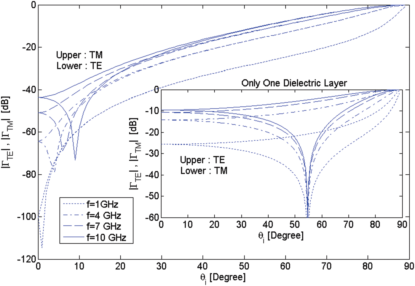
Fig. 7. The |ΓTE| and |ΓTM| of a DFR with d = 5 mm, N = 4 and μ r = ɛ r = 2 (θ 0 = 0°) and those of a homogeneous dielectric layer with d = 5 mm and ɛ r = 2.

Fig. 8. The |ΓTE| and |ΓTM| of a DFR with d = 5 mm, N = 4, and μ r = ɛ r = 1.2 (θ 0 = 0°) and those of a homogeneous dielectric layer with d = 5 mm and ɛ r = 1.2.

Fig. 9. The |ΓTE| and |ΓTM| of a DFR with d = 5 mm, N = 4, and μ r = ɛ r = 2 (θ 0 = 0°).

Fig. 10. The |ΓTE| and |ΓTM| of a DFR with d = 5 mm, N = 4, and μ r = ɛ r = 1.2 (θ 0 = 0°).
Finally, Fig. 11 demonstrates the propagation of TE polarized wave, at frequency 10 GHz and θi = 20°, created by a horn antenna with ±20° beam-width in front of a DFR (d = 5 mm, N = 4, and μ r = ɛ r = 2) and a dielectric layer (d = 5 mm and ɛ r = 2). This figure has been obtained from the full-wave simulator CST software. It is seen that the reflection of wave from DFR is much weaker than that of the dielectric layer Radome. In fact, Fig. 11 validates Fig. 7.
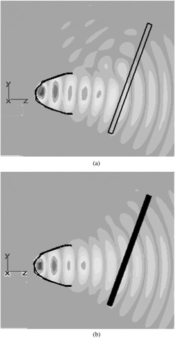
Fig. 11. The absolute of electric field for TE polarized incident wave at f = 10 GHz simulated by CST software. (a) a homogeneous dielectric layer with d = 5 mm and ɛ r = 2. (b) a DFR with d = 5 mm, N = 4, and μ r = ɛ r = 2 (θ 0 = 0°).
V. CONCLUSION
A new structure was proposed to operate as wideband and wide-angle flat Radome. In this structure several dielectric and ferrite layers are placed alternately beside each other to behave as a matched slow wave layer, while the permittivity and permeability of dielectric and ferrite layers are chosen equal to each other. The performance of the proposed structure was investigated and validated using some theoretical and simulation examples. It was observed that the reflection coefficients of DFRs are much less than those of dielectric layers with the same permittivity and thickness. Also, it was seen that as the permittivity of DFRs is decreased, useful frequency bandwidth and incidence angle range are increased.
 Mohammad Khalaj-Amirhosseini was born in Tehran, in 1969. He received his B.Sc., M.Sc., and Ph.D. degrees from Iran University of Science and Technology (IUST) in 1992, 1994, and 1998, respectively, all in electrical engineering. He is currently an Associate Professor at College of Electrical Engineering of IUST. His scientific fields of interest are electromagnetic direct and inverse problems including microwaves, antennas, and electromagnetic compatibility.
 Sayed Mohammad Javad Razavi was born in Kashan, Iran in 1976. He received the B.Sc. degree from Isfahan University of Technology (IUT), M.Sc. degree from Malek Ashtar University of Technology (MUT), Tehran, and Ph.D. degree from Iran University of Science and Technology (IUST) all in electrical engineering in 1999, 2002, and 2009, respectively. Currently, he is a researcher in EEUC/Electrical &Electronic University complex/MIUC Tehran, Iran.


