I. INTRODUCTION
Innovative and high-performance antenna systems are required in modern communication systems, as well as in a number of industrial and military applications. At the same time, new technologies and devices are emerging to comply with such specifications. In this context, electronically reconfigurable antennas are receiving increasing interest from industries active in key areas such as space and terrestrial communications, remote sensing, microwave imaging, and radar systems. Such antennas, in fact, potentially exhibit exceptional performance in scanning/tracking velocity, tolerance to vibrations, coverage modification, and robustness against interferences. Reconfigurability is typically accomplished by employing solid-state tuning devices (pin or varactor diodes, Field Effect Transistor (FET)). Recent advances in RF-MEMS (micro-electro-mechanical systems) technology eventually enable the use of such components in RF and especially in mm-wave systems. Thanks to their inherent low cost and high performance, RF-MEMS can potentially bring in completely new classes of tunable devices and circuits, particularly at high frequencies where the semiconductor-based counterparts suffer from unavoidable limitations such as loss, non-linearities, and cost. In this framework, reflectarrays (RAs) are of special interest particularly at mm-wave frequencies, where the loss associated with the feeding network makes impractical the use of directly radiating arrays.
RA antennas combine indeed the advantages of reflector antennas with those of phased arrays. In its basic form (see Fig. 1) an RA consists of a planar array of radiating elements illuminated by a primary source (the feed), similar to classical reflector antennas. The individual elements of the array are designed to scatter the incident field while impressing the appropriate phase shifts in such a way as to form a plane wave front that propagates in a prescribed direction or, more generally, to create the required radiation pattern. Various types of scattering elements can be used in the practical realization of RAs, e.g. microstrip patches or waveguide apertures, operating on linear, dual, or circular polarization. The phase shift (sometimes also the amplitude variation) produced by the radiating element can be obtained in several ways that, generally speaking, can be grouped into two main classes: in the first one, the phase shift is obtained by varying the shape of the radiating elements [Reference Martynyuk, Martinez Lopez and Martynyuk1–Reference Carrasco, Barba and Encinar9]. Reconfigurability can be achieved by integrating the tuning device within the radiating element so as to either alter its electrical properties or its geometry. Compact multi-beam RAs have been developed by Menzel et al. [Reference Menzel, Al-Tikriti and Leberer10, Reference Menzel, Pilz and Al-Tikriti11] employing a polarizing grid as a sub-reflector. Reconfigurability is obtained in [Reference Hu12–Reference Bildik, Fritzsch, Moessinger and Jakoby14] by exploiting the voltage-dependent dielectric properties of liquid crystals. Various approaches are proposed employing varactor diodes [Reference Hum, Okoniewski and Davies15–Reference Boccia, Amendola and Di Massa20] or RF-MEMS [Reference Gianvittorio and Rahmat-Samii21–Reference Perruisseau-Carrier and Skrivervik30] as tuning devices for reconfiguring the RA.

Fig. 1. RA principle of operation.
In the second class of control techniques, the radiating element is separated from the tuning element (a phase shifter), yet electromagnetically coupled to it. This approach allows one to separately design the radiating and the control sections of the antenna, without much concern – within certain limits – of the mutual interactions among them. Examples of such an approach to fixed beam RAs are given in [Reference Carrasco, Barba and Encinar31–Reference Trampuz, Hajian and Ligthart35], while electronically tunable RAs are proposed in [Reference Apert, Koleck, Dumon, Dousset and Renard36] using PIN-diodes, in [Reference Riel and Laurin37] using varactor diodes, in [Reference Marin, Mossinger, Freese, Muller and Jakoby38] using liquid crystals, and in [Reference Siegel, Ziegler, Schönlinner, Prechtel and Schumacher39–Reference Sorrentino50] using RF-MEMS. In particular, in [Reference Sorrentino, Vincenti Gatti, Marcaccioli and Mencagli46–Reference Sorrentino50], the specific research activity carried out by the University of Perugia is reported, in the framework of the European Network of Excellence AMICOM (Advanced MEMS for RF and MIllimeterwave COMmunications), which has led to the design and fabrication of two RAs operating at Ka-band, both employing nearly 1000 RF-MEMS. Concerning active architectures, General Electric Co. proposed in a patent [Reference Profera and Charles51] an active RA, including amplifiers and phase shifters on the elementary cells. Also, an active RA with MESFET amplifiers operating at X-band was demonstrated at the University of Queensland (Australia) [Reference Bialkowski, Robinson and Song52]. Finally, an active architecture based on quadrature components vector decomposition and weighting and therefore simultaneously allowing amplification and phase shift has been proposed in [Reference Cabria, Garcia, Tazon and Vassal'lo53–Reference Cabria, Garcia, Tazon, Mediavilla and Vassal'lo54].
In this paper the work performed in RAs by University of Perugia is presented. In particular, the activities carried out within the Agile Reflectarray Antennas for Security and COMmunication (ARASCOM) project [55] are reported, one of the objective being the exploitation of MEMS technology in mm-wave RA s for security imaging applications. Due to the fact that the required antenna is extremely large, a number of technical solutions have been developed. This paper presents for the first time in a complete and comprehensive way all the main aspects of the project, starting from requirements to architectural choice, MEMS design, measurements, antenna simulations, and future steps.
II. ENABLING TECHNOLOGIES FOR RECONFIGURABILITY
Different technologies can be used for the tuning elements. Each technology has a different impact on the system in terms of costs, losses, power consumption, and control complexity. Since for many practical applications reconfigurable RA s may be made of thousands of elementary cells, the adopted technology has definitely a strong impact on the overall cost. In Table 1, the main enabling technologies for reconfigurability are summarized, together with some of the key parameters that have to be considered for their selection. In this table a tentative comparison of the available technologies has been performed.
Table 1. Potential reconfigurable components and their impact on some key parameters.

*Some commercial MEMS are available from American industries. In Europe one of the most successful foundry (although not yet on the market for RF-MEMS) is the FBK-irst of Trento (Italy).
A unique advantage of RA antennas is that the packaging can be made at antenna level, or subarray level. This aspect had been exploited by University of Perugia since AMICOM project for the MEMS-based RA [Reference Sorrentino, Vincenti Gatti, Marcaccioli and Mencagli46–Reference Sorrentino50], allowing to realize an RA directly on wafer and then package the entire structure.
III. INNOVATIVE ARCHITECTURES FOR RECONFIGURABLE RAS
The design of a large reconfigurable and foldable RA antenna for broadband emergency communications in Ku-band has been carried out within the ESA project named RESKUE (ESA contract n° 22078/08/NL/ST). Due to the extremely large number of elements, the reconfigurability with 1-bit phase resolution has been successfully investigated. Thanks to the non-quadratic phase distribution produced by the feed over the antenna aperture, a phase resolution of 1 bit can effectively steer the beam without grating lobes with a gain decrease of only 3 dB and virtually no loss of pointing angle accuracy. Reconfigurability was obtained through the employment of PIN diodes, though the adopted architecture may be also compatible with other technologies, such as RF-MEMS. Details of the project and most recent achievements are reported in [Reference El Gannudi, Vincenti Gatti, Tomassoni and Sorrentino56, Reference Montori57].
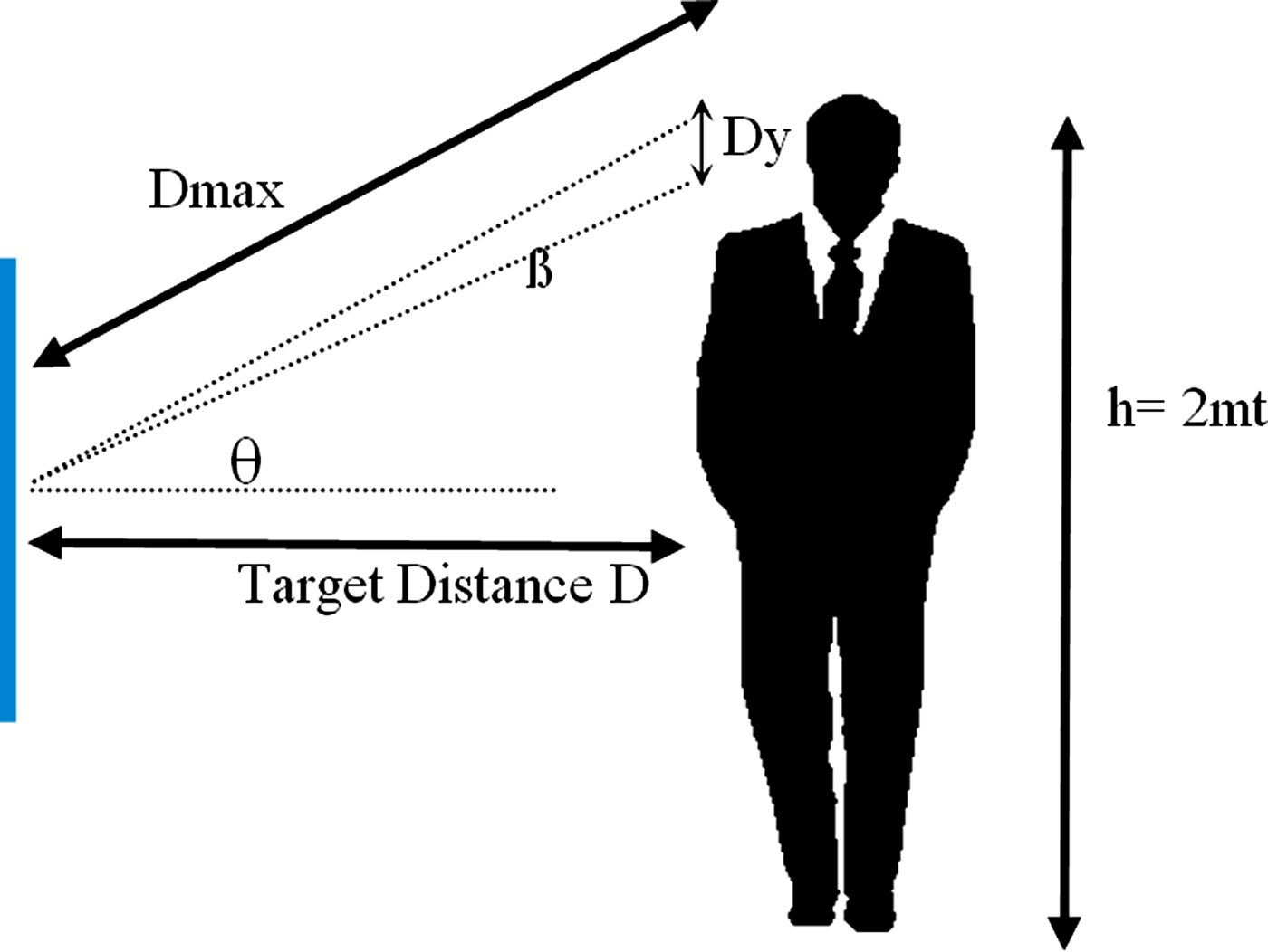
In the frame of FP7 project ARASCOM (‘MEMS and liquid crystal based’) [58], one objective is to demonstrate the feasibility of a large MEMS-based RA for imaging systems at 77 GHz. The objective of the project is the antenna, not the imaging system by itself. Therefore, in this paper only the aspects concerning the antenna design are covered. The antenna under development, meant for airport security applications, shall give a resolution of nearly 2.5 cm in a target (human body) of maximum 2 m height by 1 m width (this requirement is given by one of the industrial partner of the consortium, Selex-SI – Italy). The first step in the design procedure is to estimate the dimensions and the characteristics of the required array; to this end, a few computations are required, reported in subsequently.
Let us consider a rectangular array: the size can be carried out independently for the two dimensions, horizontal and vertical. With reference to Fig. 2 the 3 dB beamwidth of a vertical array pointing toward θ is given in the far field by the following formula [Reference Balanis59]:

Fig. 2. System dimensioning.
On the target the observed spot has a width of
where H is the target height. By combining (1) and (2) we obtain
Once the half-power spot width is fixed, the number of elements only depends on the maximum steering angle θ. Figure 3 shows the variation of the required number of elements for a given resolution (2.5 cm) versus θ. The minimum value of N is obtained when the target is seen under 35.32° maximum steering angle (view angle of 70.64°) and is nearly 180°. This means that the antenna shall be placed at 1.41 m from the target.

Fig. 3. Required element number with respect to the maximum angle of observation of the target. The minimum is at 35.32°.
Obviously the spot width varies while scanning the target (Fig. 4). By performing the same computations for the azimuth plane, we obtain a value of nearly 110. All these computations have been made assuming a pattern in the far field. By applying the near-field correction, however, similar values are obtained. Nevertheless, to the purpose of the ARASCOM project it is sufficient for the moment to consider an RA of 180 × 110 elements, i.e. nearly 20 000 radiating elements.

Fig. 4. Variation of the spot width along the target height for N = 180.
Such an array presents many critical aspects that have been handled by developing a number of solutions:
1) The elementary cell has 1-bit phase resolution. As already mentioned, this approach can effectively produce a beam steering without grating lobes, with an enormous cost and complexity reduction.
2) The phase-shifting circuit is placed underneath the radiating element (a patch) so as to allow for a significant reduction of the cell area. Such architecture makes it possible to individually fabricate the radiating elements as small chips that can be later assembled in a very large RA [Reference Marcaccioli, Montori, Gatti, Chiuppesi, Farinelli and Sorrentino60].
3) Each elementary cell employs two MEMS. By separating the illumination and exploiting the fact that an MEMS can be actuated by either a positive or a negative voltage, the number of biasing lines is reduced from theoretical 39 600 to just 400.
4) In order to obtain (3), the MEMS have been designed in such a way as to have DC pads electrically isolated from RF pads.
In the following the details of the elementary cell, the adopted biasing network, the RF-MEMS design, manufacturing, and test are provided.
A) Slotline elementary cell architecture
The developed elementary cell is depicted in Fig. 5. It is made of a square patch antenna realized on the top layer of a thin quartz substrate (h = 300 µm). The patch is slot coupled to the 1-bit phase-shifting circuit realized in slot-line technology on the backside of a quartz substrate. The slot-line layer (or phase-shifting layer) consists of three lines connected in T configuration; each line is terminated with a U-shaped slot, so as to be coupled to one of the two linear polarizations that can be radiated by the patch. A fourth dummy slot (not connected) is used to make the layout symmetrical so that the radiation diagram of the elementary cell is identical for both polarizations.

Fig. 5. Sketch of the elementary cell (a) and picture of the phase shifting layer (b). The dotted line indicates the square patch located on the radiating side of the cell.
A pair of MEMS switches are integrated in the phase-shifting layer; the MEMS bridges are anchored at the substrate and short circuit the two metal planes when pulled down. The control of the cell is obtained by activating the switches so as to obtain an single Pole Double Through (SPDT) that alternatively connects slot 1 with slot 2 or slot 3.
When a linearly polarized field, either vertical or horizontal, illuminates the elementary cell the orthogonal polarization is back-radiated, independently of the cell state. Since slots 2 and 3 feed the patch at opposite edges, in the two cases the reflected field has opposite directions, equivalent to 180° of phase difference.
It is worth observing that the phase-shifting circuit has been designed entirely confined underneath the patch so that the area of the elementary cell does not exceed 1 mm2, i.e. a quarter of wavelength at 76.5 GHz.
The elementary cell was simulated full wave by exciting it with a linear polarized plane wave. Electric and magnetic probes in both polarizations have been used to extract the two-port S-parameters of the cell, being the two plane-wave ports associated to the two orthogonal polarizations. Simulations have been performed with Floquet ports and periodic boundary conditions in Ansoft HFSS v11. Figure 6 shows the S-parameters of the elementary cell: it is evident that the elementary cell properly rotates the polarization of the field within a bandwidth of nearly 20 GHz (S11 and S22 lower than −10 dB). The structure was simulated in both MEMS configurations (MEMS simulated as ideal short circuits). The phase of the cross-polarization reflection coefficient in both cell configurations is also shown: as expected, a 180° flat phase-shift response is observed, even outside the patch bandwidth.

Fig. 6. Amplitude of the elementary cell scattering parameters (a) and phase of cross-polarization reflection coefficients of the cell in both possible configurations (b). Port 1 and Port 2 are the plane waves associated with the two orthogonal polarizations of the field.
To validate the principle of operation of the elementary cell, a board made of 16 × 16 elementary cells all in the same configuration has been realized (Fig. 7).

Fig. 7. Manufactured quartz wafer.
The MEMSs have been replaced by short/open connection. It can be noticed from Fig. 8 that, by simply rotating the elementary cell 90°, the two configurations corresponding to the two states of the elementary cell are obtained. In other words, by physically rotating the cell 90° a 180° of phase-shift is obtained; this principle has been used for the measurements.

Fig. 8. Phase-shifting layer of the cell with rotation of 0° (a) and 90° (b).
The free-space reflection coefficient of the board is measured in a small anechoic chamber with a couple of horns, as shown in Fig. 9. Both the cross-pol and co-pol reflection coefficient of the cell have been measured with the aid of a waveguide twist.

Fig. 9. Measurement setup and antenna under test (AUT).
Figure 10(a) shows the comparison between measured and simulated results. In both cases less than −20 dB co-polarization reflection coefficient is measured at center frequency (76.5 GHz). Losses are calculated around 3 dB at center frequency. This value is affected by uncertainty due to the approximate knowledge on the conductivity and roughness of the silver metal plate and the gold of the antenna.
The relative phase difference between cross-polarization reflection coefficients of the cell in both states has been evaluated: Fig. 10(b) shows 6° maximum measured error with respect to the ideal case (180°) and an average 177° relative phase shift. This can be easily ascribed to small errors in the placement during board rotation (i.e. to change the state): at 76.5 GHz, 1° phase shift can indeed be easily obtained with a 10 µm shift in the RA position.

Fig. 10. Simulated and measured deembedded reflection coefficients of 16 × 16 RA (a). Measured relative phase difference between cross-polarization reflection coefficients of the cell in both polarizations (b).
B) Bias control architecture
As highlighted in Section III(A), the elementary cell has been optimized for minimum dimensions (1 × 1 mm2). In this manner it is possible to fabricate thousands of small chips containing both the elementary cell and the phase-shifting circuitry. These chips will be then mounted in a special printed circuit board, where cavities properly (half-a-wavelength) spaced are drilled (Fig. 11). This board will also have printed biasing lines that will be wire-bonded to the chip and provide the necessary connection from the external biasing device to the single chip. A large RA can also be realized by properly spacing thousands of small chips over a suitable support realized on a low-cost material.

Fig. 11. Sketch of the supporting board with cavities and printed biasing lines and with elementary cells inserted in the cavities.
Ground continuity between chips and supporting board is also realized through wire bondings (Fig. 12). This solution allows one to obtain a considerable reduction of design complexity thus of the RA fabrication cost.

Fig. 12. Sketch of the elementary cell inserted in the cavity: (a) top view and (b) bottom view.
Even by exploiting the 1-bit solution, the practical control of tens of thousands of elements is a critical issue. The control circuitry can be dramatically simplified by exploiting the concept of separable illumination: the phase shift of the generic (m, n) cell necessary to steer the beam of the RA in any far-field direction (θ 0, φ 0) can be expressed in the form
where α m and β n are the phases imposed by the row m and column n, respectively.
By taking advantage of the 1-bit phase resolution of the cells, an interesting solution for the control architecture has been carried out. Table 2 shows the phase that each cell shall assume depending on the column and row state, together with the MEMS state and assuming that when the lines are set to high voltage the phase is 180°. Note that one of the MEMS (i.e. MEMS#1) of the cell shall exhibit the equivalent of an XOR function while the other has a complementary behavior: this can be very easily accomplished by connecting the two pads of MEMS#1 at the row and column biasing lines, respectively. In this manner, when the column and row have the same biasing voltage (States 2 and 4), MEMS#1 is not actuated whereas when they have different voltages (States 1 and 3) MEMS#1 is actuated either by a positive or negative potential. MEMS#2 should exhibit the opposite behavior: this can be accomplished by still connecting one of its pads to the row (or column) biasing line, and the other to an additional biasing column (or row) having opposite state: the total number of biasing lines is therefore M + 2*N (or 2*M + N). In our case, by setting M = 180 and N = 110 we need a total of 400 lines.
Table 2. Description of the RF-MEMS actuation with respect to the column and row state.

In Fig. 11, the bias control architecture is evident: each cell is controlled by three lines, one for the row and a complementary pair for the column. In order to realize this kind of connection, RF MEMS have been designed in such a way as to have electrical isolation between RF and DC signals, as illustrated in Section III(C).
C) MEMS design
The MEMS shunt ohmic switch has been designed in slot-line technology on 300 µm quartz substrate. The switch consists of a 410 µm × 90 µm gold membrane clamped on the substrate at both extremities and 3 µm suspended above a 32 µm-wide slot line. Two windows have been etched away from the slot metallization to accommodate the bridge anchors as well as the lateral activation electrodes. When the switch is in the up position (OFF-state) the signal can flow along the transmission line; in contrast when it is activated (ON-state) it short circuits the two-slot metallizations at the two contact points shown in Fig. 13. In order to keep separated the DC and RF signals, two DC-blocks have been integrated in series with the switch contacts, providing a capacitive short circuit at 76.5 GHz. Thick silicon oxide (600 nm-thick –low-temperature oxide) has been used as a dielectric for the MIM capacitors to guarantee no break down up to high polarization voltages (>100 V).

Fig. 13. Schematic side view of the switch.
The switch has been modeled by using Ansoft HFSS v.11; the simulated current distribution and performance for both switch states are shown in Figs 14 and 15.

Fig. 14. Simulated current distribution on the shunt MEMS ohmic switch in ON-state (a) and OFF-state (b).

Fig. 15. Simulated reflection coefficients and insertion loss of simulated switch in ON-state (a) and OFF-state (b).
D) MEMS manufacturing and testing
The slot-line W-band MEMS switches and the MEMS-based radiating cell unit have been monolithically manufactured on a 300 µm-thick Quartz substrate by using the eight mask FBK RF MEMS process. The process allows the electro-deposition of two gold layers of different thicknesses for highly complex movable bridges and microstrip lines. The air bridges are realized without the need of any planarization steps by using a 3 µm-thick photoresist as the sacrificial layer. The bridge release is done with a modified plasma etching process in order to avoid sticking problems. The bias network is realized by depositing a high-resistivity 0.63 µm-thick poly-silicon layer covered with silicon oxide for isolating the DC from the RF lines.
This layer is also used for realizing the stopping pillars used in the capacitive switches and the contact bumps for the ohmic switches. The process allows the monolithic manufacturing of both ohmic and capacitive switches. Low-temperature oxide is used as a dielectric for capacitive switches as well as MIM capacitors. A third gold layer is deposited for the realization of low-resistance metal-to-metal electro-mechanic contacts for ohmic switches. In order to mitigate dielectric charging phenomena, the dielectric has been removed from the surface of the activation pads. Mechanical stoppers have been patterned in the pads to prevent the contact between the down-state bridge and the dielectric-less pads. The mechanical stoppers have been realized by stacking polysilicon, dielectric and gold layer to reach a stopper thickness about 0.55 µm higher than the electrode thickness. A photo of the manufactured device is shown in Fig. 16.

Fig. 16. Photo of air-bridge shunt ohmic switch in slot-line technology.
DC measurements have been performed to characterize the behavior of the slot-line switches.
Actuation and de-actuation voltages of about 60 and 50 V have been recorded, with no evident voltage drift due to dielectric charging in short-time tests. When activated, the measured contact resistance between the MEMS bridge and the floating metal is about 1 Ω ensuring a good short circuit between the two metal planes.
The radiation pattern of an RA with square aperture of dimensions 80 mm × 80 mm (40 × 40 cells) has been evaluated in the far field starting from an accurate full-wave simulation of a single cell in its final and most realistic configuration, where real MEMS and wire bondings have been included. A horn operating at 76.5 GHz is used in simulations as a feeder.
The 1-bit phase distribution for a main beam direction of 30° in elevation and 0° in azimuth is shown in Fig. 17. Figure 18 shows the co- and cross-polarization radiation patterns. A directivity of nearly 40.9 dB is expected with −25 dB of maximum side-lobe level.

Fig. 17. One-bit phase distribution on the 180 × 110 RA.

Fig. 18. Co-pol. and Cross-pol radiation patterns of 40 × 40 RA along azimuth (a) and elevation cut and bi-dimensional plot of the Co-pol radiation pattern (b).
IV. Conclusions
In this paper the most recent results and achievements carried out at the University of Perugia on the development of innovative architectures, solutions, and technologies for large reconfigurable RA antennas at mm-wave frequencies have been presented. In particular, the design of a large beam steerable RA in W-band for imaging application has been presented, the development being carried out within the ARASCOM project (7th European framework program). The design has required a number of innovative steps: the elementary cells have 1-bit phase resolution, and have been conceived in small chips that can be produced in thousands of pieces and then placed in a special printed circuit board that ensures both the proper spacing and the biasing. The elementary cell basic design has been successfully demonstrated by fabricating and measuring a 16 × 16 board. The exploitation of 1-bit phase resolution, a separable illumination approach, and the MEMS property of being toggled either by a positive or negative voltage has made it possible to arrange a very simple control strategy that reduced the number of biasing lines from 39 600 to 400. Finally, MEMS switches have been specially designed for the elementary cell in slot-line technology, with DC and RF pads electrically isolated. MEMS cells have been already fabricated, and their assembly in a first fully reconfigurable 40 × 40 RA prototype is currently ongoing in SELEX-SI, partner of the consortium.
ACKNOWLEDGEMENTS
This work has been performed in the frame of the ARASCOM project supported by the 7th European framework program, contract no. 222620. The authors wish to thank Flavio Giacomozzi and Benno Margesin from Fondazione Bruno Kessler (FBK-irst), Trento, Italy for manufacturing the devices.
 Simone Montori was born in Spoleto, Italy, on August 26, 1981. He received his masters degree (with honors) in electronic engineering from the University of Perugia, Perugia, Italy, in 2006. In 2006, he joined the Department of Electronic and Information Engineering (DIEI) of the University of Perugia (Italy) as a research student. He is currently pursuing his Ph.D. in information engineering. His main research interests include reflectarrays and reconfigurable antenna systems.
 Elisa Chiuppesi was born in Orvieto, Italy, on January 7, 1981. She received the Laurea degree in electronic engineering from the Università degli Studi di Perugia, Perugia, Italy in 2008. In 2008, she joined the Department of Electronic and Information Engineering (DIEI) of the University of Perugia (Italy) as a research student, under the advice of Prof. Roberto Sorrentino. Her research activities include characterization and measure of the devices RF MEMS and design of MEMS devices.
 Luca Marcaccioli received the Laurea degree cum laude in electronic engineering from the University of Perugia, Italy, in 2002, then he joined the Department of Electronic and Information Engineering (DIEI) of the University of Perugia (Italy), and in 2005 he received his Ph.D. degree. In September 2007, he was the co-founder of the RF Microtech srl, a spin-off company of the University of Perugia. Dr. Marcaccioli is a member of the European Microwave Association. He was a co-recipient of the Young Engineers Prize presented at the 2007 European Microwave Conference (EuMC), Munich, Germany, and the co-recipient of the 2008 Best Student Paper Award (First Place) presented at the IEEE Microwave Theory and Techniques Society (IEEE MTT-S) International Microwave Symposium (IMS), Atlanta, GA.
 Paola Farinelli was born in Assisi, Italy, on September 19, 1978. She received the Laurea degree (with distinction) in electronic engineering from the University of Perugia, Italy, in 2002. In 2002, she joined the Department of Electronic and Information Engineering of the University of Perugia as a Ph.D. student. In 2003, she conducted research work at the “Institut de Recherche en Communications Optiques at Microondes (IRCOM)”, Limoges University, (France). From November 2004 to May 2005, she has been a visiting researcher at VTT Millilab (Finland). In January 2006, she received her Ph.D. degree and is currently working at the University of Perugia as a contract researcher. Her research activity includes the electromagnetic modeling and design of reconfigurable RF MEMS devices such as SPDT switches, phase shifters, power dividers, and filters.
 Roberto Vincenti Gatti received the Laurea degree summa cum laude from the University of Perugia, Italy, in 2000, and Ph.D. degree from the same University in 2007. Since 2007, he has been a Research Assistant at the University of Perugia. He lectures Antennas and tutors Wireless Systems and Design of RF Circuits. His current research activities include the analysis, modeling, and design of phased arrays and reflectarrays, phase-only and phase/amplitude synthesis and optimization techniques for linear, planar, and conformal arrays, design of phase shifters and passive microwave and millimeter-wave components, and investigation of innovative architectures for MEMS or diode-based reconfigurable devices. He has produced more than 60 publications and presentations in international conferences and has developed a rigorous and efficient CAD tool for the analysis and design of large electronically scanning slotted waveguide antennas (www.swan-soft-com). He is the vice president and a member of the board of directors of RF Microtech srl.
 Roberto Sorrentino (M'77–SM'84–F'90) received his doctorate degree in electronic engineering from the University of Rome “La Sapienza”, Rome, Italy, in 1971. In 1974, he became an Assistant Professor of microwaves with the University of Rome “LaSapienza”. He was an Adjunct Professor with the University of Catania, the University of Ancona, and the University of Rome “La Sapienza” (1977–1982), where he then was an Associate Professor from 1982 to 1986. In 1983 and 1986, he was a Research Fellow with The University of Texas at Austin. From 1986 to 1990, he was a Professor with the University of Rome “Tor Vergata”. Since November 1990, he has been a Professor with University of Perugia, Perugia, Italy, where he was the Chairman of the Electronic Department, Director of the Computer Center (1990–1995), and Dean of the Faculty of Engineering (1995–2001). In 2007, he founded RF Microtech s.r.l., Perugia, Italy (a spinoff of the University of Perugia). He has authored or coauthored over 100 technical papers in international journals and 200 refereed conference papers. He edited a book for the IEEE Press and coauthored three books on advanced modal analysis (2000), microwave filters (2007), and RF and microwave engineering (2010). His research activities have been concerned with various technical subjects such as the EM wave propagation in anisotropic media, the interaction of EM fields with biological tissues, but mainly with numerical methods and computer-aided design (CAD) techniques for passive microwave structures, and the analysis and design of microwave and millimeter-wave circuits. In recent years, he has been involved in the modeling and design of RF microelectromechanical systems (RF-MEMS) and their applications on tunable and reconfigurable circuits and antennas. Dr. Sorrentino was the International Union of Radio Science (URSI) vice chair (1993–1996) and chair (1996–1999) of Commission D (Electronics and Photonics). Since 2007, he has been the president of the Italian Delegation of URSI. In 1998, he was one of the founders of the European Microwave Association (EuMA) and was its President from its constitution until 2009. In 2002, he was among the founders and was the first president of the Italian Electromagnetic Society (SIEm), which he chaired until 2008. From1998 to 2005, he was a member of the High Technical Council, Italian Ministry of Communications. From January 1995 to April 1998, he was the editor-in-chief of the IEEE MICROWAVE AND GUIDED WAVE LETTERS. From 1998 to 2005, he was on the Administrative Committee of the IEEE Microwave Theory and Techniques Society (IEEE MTT-S). He is a member of Technical Committees MTT-15 on Field Theory and MTT-1 on Computer-Aided Design. In 1993, he was the recipient of the IEEE MTT-S Meritorious Service Award. In 2000, he was one of the recipients of the IEEE Third Millennium Medal. In 2004, he was the recipient of the Distinguished Educator Award of the IEEE MTT-S.