Introduction
Transitions are necessary when different types of transmission lines are connected to each other. For designing wideband transitions, not only the characteristic impedances but also the propagation modes between the connected transmission lines need to be matched. With carefully designed transitions, the electromagnetic waves can be guided smoothly through different structures and the propagation mode is converted. The mismatch of either characteristic impedance or propagation mode result in a narrowband transition with high insertion loss [Reference Mao, Hwang, Wu and Chen1]. Transmission lines such as microstrip line, coplanar waveguide (CPW), coplanar stripline (CPS), and asymmetric coplanar stripline (ACPS) used for microwave integrated circuits (MICs) as well as monolithic microwave integrated circuits (MMICs) mainly rely on planar structures due to their fabrication processes. Compared with microstrip line, CPW, and CPS have low transmission loss and their characteristic impedances are less sensitive to the thickness of the substrate which makes it possible to taper the dimensions of the transmission lines without affecting the characteristic impedance. It also makes CPW and CPS versatile for designing components and chips based on different substrates and packaging them into a system. In communication systems, CPW in a ground-signal-ground (GSG) configuration is normally used for designing amplifiers [Reference Deal, Mei, Radisic, Leong, Sarkozy, Gorospe, Lee, Liu, Yoshida, Uyeda and Lai2–Reference Urteaga, Griffith, Seo, Hacker and Rodwell5], frequency doublers [Reference Zhurbenko, Johansen, Squartecchia, Midili, Rybalko, Riet, Dupuy, Nodjiadjim and Konczykowska6, Reference Ye, Yu, Tang, Drouin and Gu7], mixers [Reference Johansen, Vidkjaer, Krozer, Konczykowska, Riet, Jorge and Djurhuus8, Reference Reck, Zemora, Schlecht, Dengler, Deal and Chattopadhyay9], power digital to analog converters [Reference Gnauck, Winzer, Konczykowska, Jorge, Dupuy, Riet, Charlet, Zhu and Peckham10, Reference Mardoyan, Mestre, Rios-Müller, Konczykowska, Renaudier, Jorge, Duval, Dupuy, Ghazisaeidi, Jennevé, Achouche and Bigo11], and interposer connections between different components [Reference Jiang, Krozer, Bach, Mekonnen and Johansen12, Reference Dong, Johansen, Zhurbenko, Beretta, Vannucci and Locatelli13]. Being different from CPW, CPS as well as ACPS are in a ground-signal (GS) configuration and they are used for designing baluns [Reference Chiou, Chang and Lin14–Reference Lin, Wang, Zhang and Hong17], antennas [Reference Anagnostou, Morton, Papapolymerou and Christodoulou18–Reference Roshna, Deepak, Sajitha and Mohanan20], and the electrodes of Mach-Zehnder modulators (MZMs) [Reference Akiyama, Itoh, Takeuchi, Kuramata and Yamamoto21–Reference Ogiso, Ozaki, Ueda, Kashio, Kikuchi, Yamada, Tanobe, Kanazawa, Yamazaki, Ohiso, Fujii and Kohtoku23].
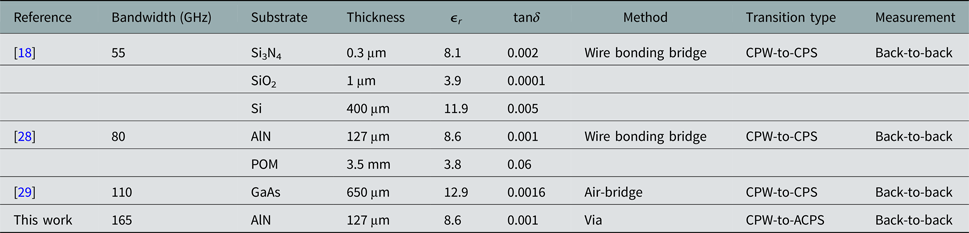
For system integrations, it becomes critical for connecting the output of a driver to the input of a MZM or designing an on-chip dipole antenna at the output of a power amplifier. Under these circumstances, the transitions between GSG and GS are necessary. With the ever increasing demand worldwide for high-speed communication, the ultra-wideband transitions between different types of planar transmission lines with the ability of supporting transmissions from DC to terahertz (THz) frequencies are under intensive study. The challenges in designing wideband transitions include characteristic impedance mismatch, mode conversion loss, resonance, and radiation. Several publications can be found for CPW-to-microstrip [Reference Wu, Hsu, Chang, Kärnfelt, Zirath, Starski and Wu24, Reference Zhou and Melde25], CPW-to-stripline [Reference Valois, Baillargeat, Verdeyme, Lahti and Jaakola26, Reference Bhutani, Goettel, Thelemann and Zwick27], and CPW-to-CPS [Reference Anagnostou, Morton, Papapolymerou and Christodoulou18, Reference Dong, Johansen, Zhurbenko and Hanberg28, Reference Kim, Jeong, Lee, Kim, Lim, Seo and Nam29] transitions while rarely for CPW-to-ACPS transitions. A transition between CPW and CPS used for feeding a multiband dipole antenna was published in [Reference Anagnostou, Morton, Papapolymerou and Christodoulou18]. By using wire bonding bridges, the proposed CPW-to-CPS transition based on silicon substrate achieves a bandwidth up to 55 GHz. In [Reference Dong, Johansen, Zhurbenko and Hanberg28], the designed CPW-to-CPS transition based on aluminum nitride (AlN) substrate with wire bonding bridges can support transmissions from DC to 80 GHz which is used for feeding an indium phosphide (InP) MZM. According to [Reference Kim, Jeong, Lee, Kim, Lim, Seo and Nam29], by using reformed air-bridge the demonstrated CPW-to-CPS transition based on gallium arsenide (GaAs) substrate exhibits a bandwidth up to 110 GHz.
The purpose of this paper is to introduce an ultra-wideband CPW-to-ACPS transition based on AlN substrate which can be used as an interposer connection between a driver and an InP MZM. The concepts of designing CPW, ACPS, and CPW-to-ACPS transition are explained. The effect of adding vias all the way along the ground traces is also discussed. The design of CPW-to-ACPS transition with vias going through AlN substrate is demonstrated in detail and the magnitude of electric field distributions at different cross-sections of the transition are illustrated. The proposed CPW-to-ACPS transition is fabricated and measured in a back-to-back configuration. The simulation and measurement results are compared. To the best of our knowledge, the proposed CPW-to-ACPS transition with vias achieves the largest bandwidth ranging from DC to 165 GHz.
CPW and ACPS design considerations
CPW with vias
For a conventional CPW, two ground traces are located alongside the signal trace forming a GSG structure and a quasi-transverse electromagnetic mode can be supported. Since the characteristic impedance of a CPW is mainly determined by the width of the signal trace and the width of the gaps between the signal and ground traces, the same characteristic impedance can be achieved by CPWs with different dimensions on the same substrate. Though the ground traces play a minor role in affecting the characteristic impedance, it has to be wide enough in order to support the propagation mode since the electromagnetic waves mainly exist in the gaps. The CPW with vias based on AlN substrate shown in Fig. 1 is designed as a part of the CPW-to-ACPS transition.

Fig. 1. Designed CPW with vias based on AlN substrate.
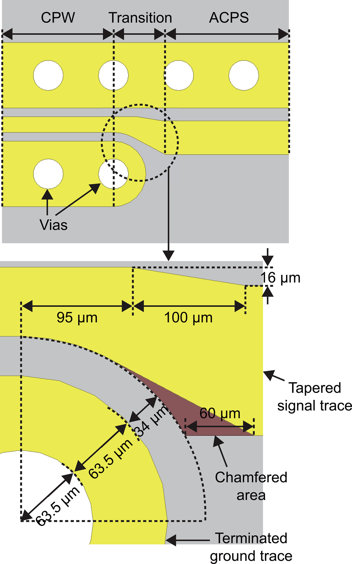
The characteristic impedance of the CPW is designed to be 50 Ω based on AlN substrate with a thickness of 127 μm. The dielectric constant (ε r) and dissipation factor (tanδ) of the substrate are 8.6 and 0.001, respectively. There are two conductor layers where the CPW is patterned on the top layer and the bottom layer works as a ground plane. The conductor is gold and the skin depth is calculated to be 0.18 μm at 170 GHz. In order to guarantee reasonable performances at low frequencies, the thickness of the conductor layers is designed to be 1.2 μm. Unlike conventional CPW structure, hollow plated vias are added along the ground traces going through the substrate and connecting the ground traces on the top to the ground plane on the bottom. The vias plated with gold are placed as close to the gaps as possible and the ground traces are designed as narrow as possible in order to suppress parasitic modes. Due to fabrication limitations, the diameter of the vias cannot be smaller than the thickness of the substrate and the edge of the vias should be at least 63.5 μm away from the edge of the conductor. As a result, for the designed CPW with vias, the width of the signal trace is 60 μm and the width of the ground trace is 254 μm with a gap width of 34 μm. The diameter of the vias is 127 μm and the center-to-center distance between two vias is 254 μm. The length and width of the substrate are 1.524 and 1.4 mm, respectively.
The designed CPW with vias is analyzed using High-Frequency Structural Simulator (HFSS). In the simulation, an air cavity with radiation boundary conditions is added on the top of the substrate representing the actual circumstance. Lumped ports and vertical perfect electric conductor (PEC) bridges are used as the excitation scheme where the PEC bridge connects to the ground traces and it is selected to be the reference. The port is assigned to the surface between the signal trace and the PEC bridge. Besides, the sheet inductance introduced by the lumped port is calibrated out from the simulation results. Figure 2 shows the simulated scattering parameters of the designed CPW from DC to 170 GHz. The return loss remains better than 19.6 dB while the insertion loss is <1.3 dB in the whole frequency range.

Fig. 2. Simulation results of the designed CPW.
ACPS with vias
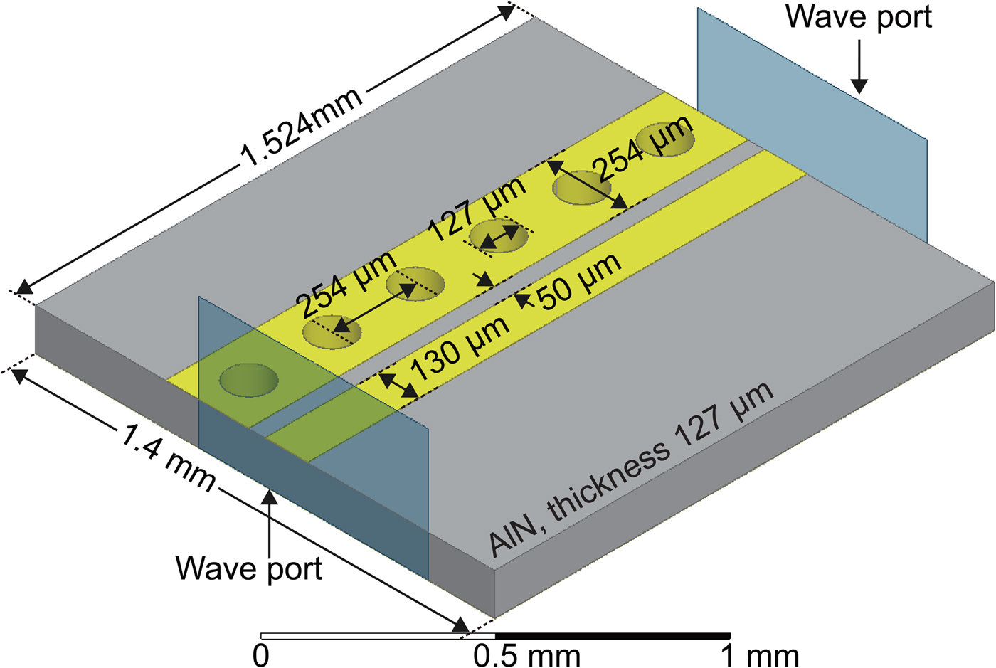
When there is only one ground trace alongside the signal trace, it forms a GS structure. For an ACPS, the widths of the signal and ground traces are different and the electromagnetic waves exist in the gap between the signal and ground traces. In order to estimate its performance at such high frequencies, an ACPS with vias based on AlN substrate is designed by using HFSS as a part of the CPW-to-ACPS transition. Figure 3 shows the simulation structure of the designed ACPS with vias. The substrate, conductor layers, and vias are the same as they used for designing the CPW. The width of the ground trace is limited to 254 μm at the minimum due to the hollow plated vias and the width of the signal trace is 130 μm with a gap width of 50 μm.

Fig. 3. Designed ACPS with vias based on AlN substrate.
In the simulation, an air cavity located on the top of the substrate with radiation boundary conditions is included for accuracy improvement. Wave ports are used as the excitation scheme. In order to generate the port field correctly, the ground trace as well as the bottom ground plane are touched by the edges of the wave port and they are selected to be the reference. Besides, the wave port needs to be large enough so that the electromagnetic waves would not couple to the edges instead of the ground trace. The designed ACPS is simulated from DC to 170 GHz and the results are shown in Fig. 4. The simulation exhibits a return loss of 13.5 dB and an insertion loss of 0.5 dB.
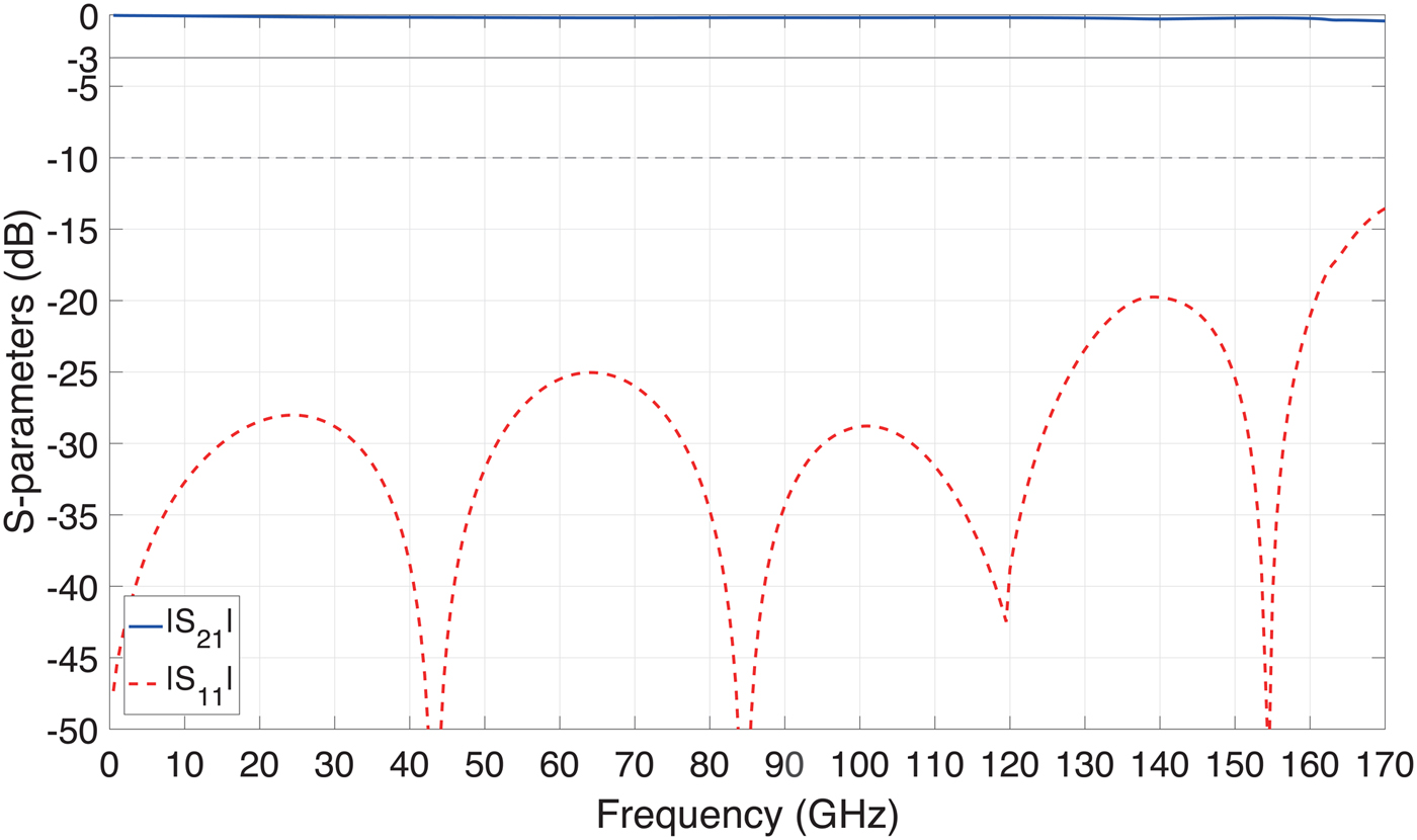
Fig. 4. Simulation results of the designed ACPS.
CPW-to-ACPS transition with vias
Design concepts
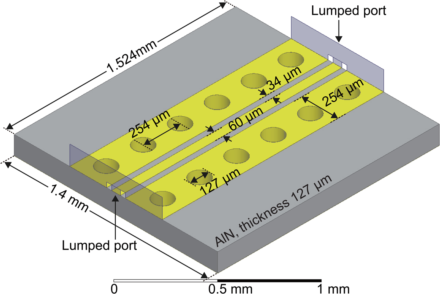
Based on the designed CPW and ACPS, a transition between CPW and ACPS is proposed with the purpose of achieving a transmission bandwidth from DC to 170 GHz. When a CPW is connected to an ACPS, one of the ground traces has to be terminated while the signal trace and the gap need to be tapered for compensating the differences in dimensions. In order to design a transition with large bandwidth, not only the characteristic impedances need to be matched but also the propagation mode must be converted smoothly. The proposed CPW-to-ACPS transition with vias is demonstrated in detail in Fig. 5.

Fig. 5. Proposed CPW-to-ACPS transition with vias.
The CPW and ACPS in the proposed transition are designed to be 50 Ω and their dimensions are shown in Figs 1 and 3, respectively. The hollow plated vias with a diameter of 127 μm are added all the way along the ground traces in order to suppress parasitic modes and increase the transmission bandwidth of the transition. For the CPW, one of the ground traces is reserved and connected directly to the ACPS without changing its dimension while the other is terminated gradually forming a semicircle. Due to fabrication limitations, the radius of the termination is 127 μm which is 63.5 μm more than the radius of the vias. For keeping the characteristic impedance matched between the CPW and ACPS, the width of the signal trace increases from 60 to 130 μm and the width of the gap between the signal and ground traces increases from 34 to 50 μm. As a result, the signal trace is tapered in on one edge where the it moves 16 μm toward the center of the signal trace and the length of the tapered structure is 100 μm. On the other edge, the signal trace is tapered out for increasing the width where it moves 86 μm away from the center of the signal trace and the tapered structure follows the shape of the terminated ground trace forming an annular ring structure with a radius of 161 μm. Besides, the dark area on the tapered signal trace in Fig. 5 is chamfered in order to reduce the reflection caused by the termination of the ground trace and its length is 60 μm.
Though methods such as wire bonding bridges and air-bridge can be used for designing wideband CPW-to-CPS transitions, the substrate needs to be thick enough to avoid parasitic modes caused by the bottom ground plane. A CPW-to-CPS transition is reported in [Reference Anagnostou, Morton, Papapolymerou and Christodoulou18] with a bandwidth of 55 GHz, the substrate consists of a silicon nitride (Si3N4) layer with a thickness of 0.3 μm, a silicon dioxide (SiO2) layer with a thickness of 1 μm, and a silicon (Si) layer with a thickness of 400 μm. As is explained in [Reference Dong, Johansen, Zhurbenko and Hanberg28], by placing a PolyOxyMethylene (POM) absorber layer with a thickness of 3.5 mm under an AlN substrate with a thickness of 127 μm, the parasitic modes are eliminated and the bandwidth of the proposed CPW-to-CPS transition increases from 63 to 80 GHz. In [Reference Kim, Jeong, Lee, Kim, Lim, Seo and Nam29], a bandwidth of 110 GHz is achieved by the designed CPW-to-CPS transition which is based on a GaAs substrate with a thickness of 650 μm.
Compared with the transitions using other methods, the proposed CPW-to-ACPS transition with vias is versatile especially for applications at THz frequencies where the thick substrate, absorber layer, and extra structures on the top of the substrate have to be avoided due to the need for compact system integrations. Besides, instead of floating, the ground traces are connected to the bottom ground plane through the vias which provides lower transmission loss and better impedance matching at such high frequencies.
Transition in a back-to-back configuration
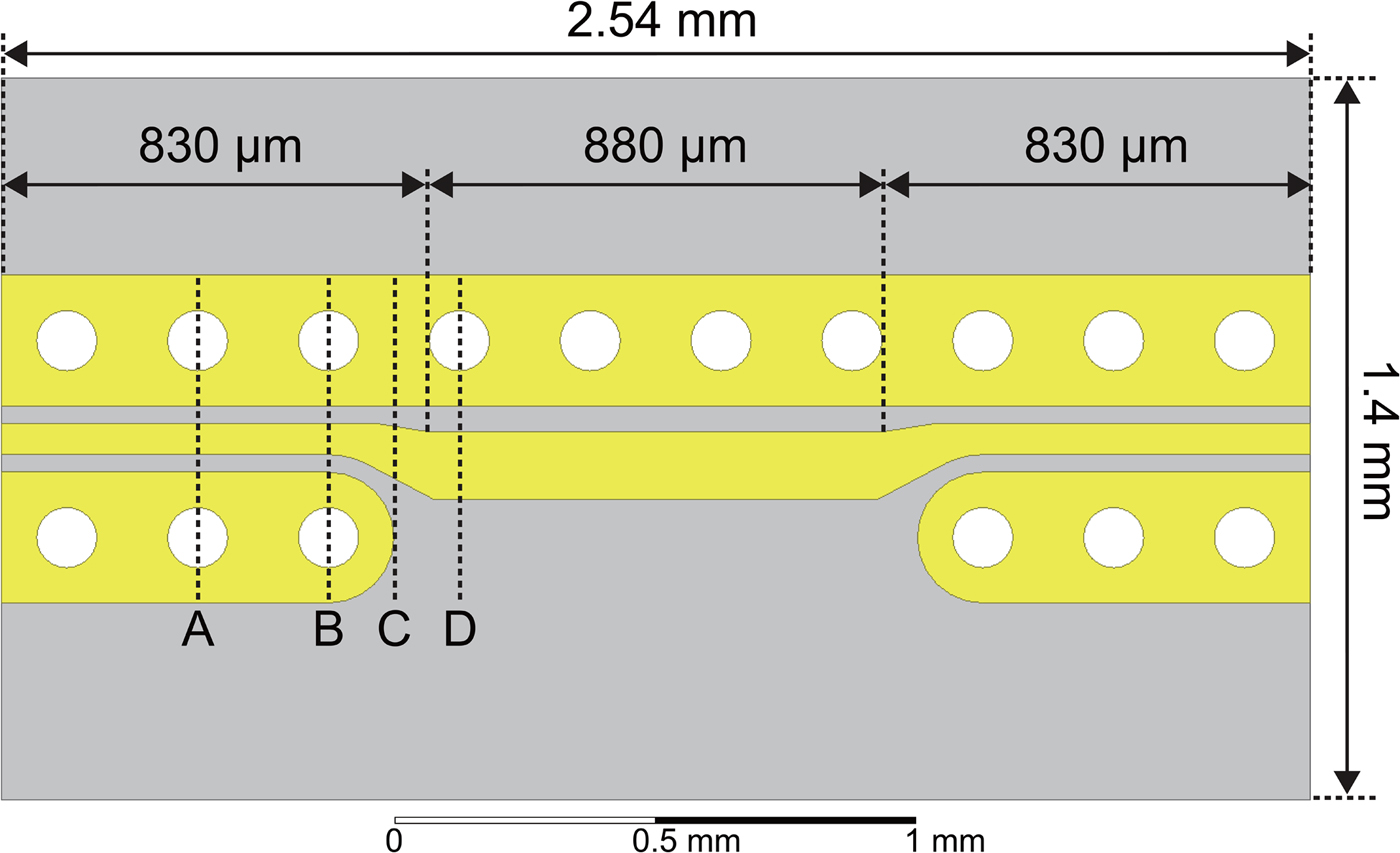
As is shown in Fig. 6, the CPW-to-ACPS transition is designed in a back-to-back configuration for easier simulation, fabrication, and measurement. There are two CPWs at the ends of the structure, an ACPS in the middle, and two transitions as interconnects. The total length and width of the AlN substrate are 2.54 and 1.4 mm, respectively.

Fig. 6. Proposed CPW-to-ACPS transition in a back-to-back configuration.
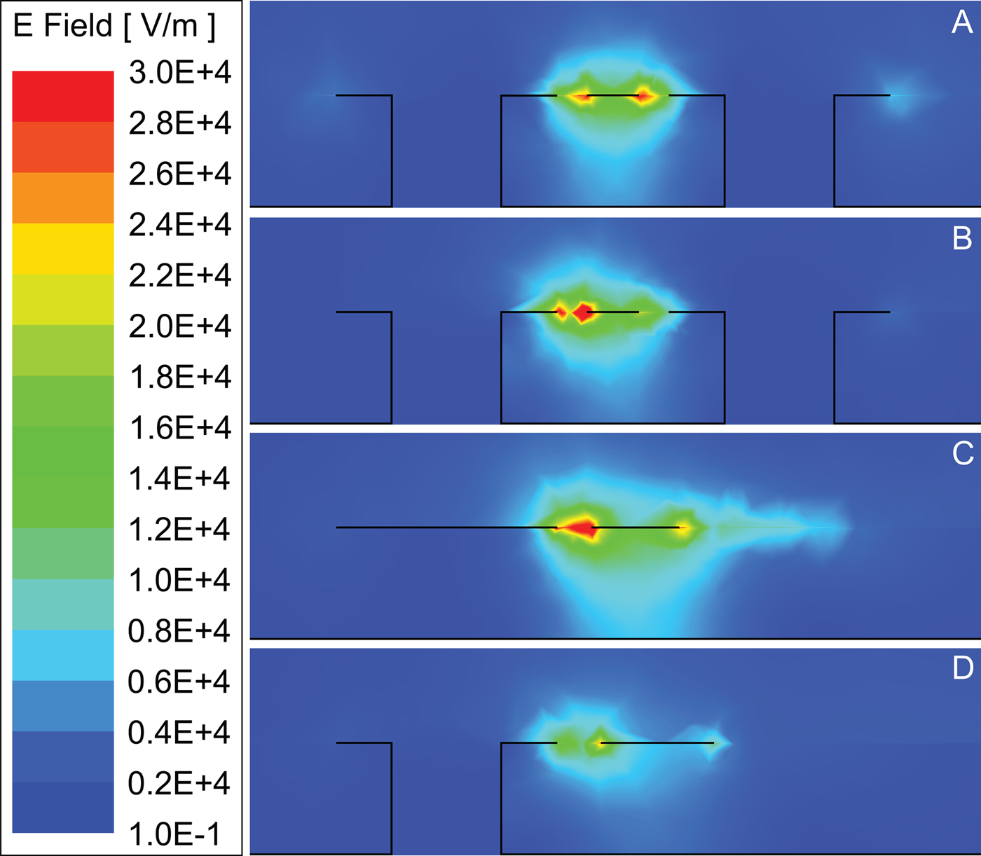
The proposed CPW-to-ACPS transition in a back-to-back configuration is simulated in HFSS using lumped ports with vertical PEC bridges. An air cavity with radiation boundary conditions and an aluminum holder are also included in the simulation representing the measurement circumstance. The magnitude of electric field distributions at different cross-sections of the proposed CPW-to-ACPS transition at 140 GHz are simulated and shown in Fig. 7. The cross-sections correspond to the locations marked with the same letters in Fig. 6. At the beginning of CPW-to-ACPS transition, the electric fields exist mainly in the two gaps between the signal and ground traces which is a standard CPW mode. When one of the ground traces is terminated gradually and the signal trace is tapered out, the electric fields start moving from one gap to another and converting to ACPS mode at the end of the transition. The magnitude of the electric fields is slightly reduced when going through the transition which is mainly caused by the impedance mismatch, mode conversion loss, and radiation. With carefully designed structures, the proposed CPW-to-ACPS transition does not introduce high transmission losses or strong reflections and the propagation modes are converted smoothly.

Fig. 7. Magnitude of electric field distributions at different cross-sections of the proposed CPW-to-ACPS transition at 140 GHz.
Fabrication and experimental results
In order to prove the concepts and validate the design, the proposed CPW-to-ACPS transition in a back-to-back configuration shown in Fig. 6 was fabricated based on AlN substrate. According to the information provided by the supplier, the thickness of the AlN substrate is 127 μm with a tolerance of 12.7 μm. The ε r and tanδ of the AlN substrate are measured at 1 MHz and they are 8.6 and 0.001, respectively. The substrate consists of 98% AlN and 2% impurities. The thickness of the gold conductors on both sides is 1.2 μm with a tolerance of 0.24 μm. The vias going through the AlN substrate are hollow plated with gold inside. The diameter of the vias is 127 μm with a tolerance of 25.4 μm. The top and bottom views of the fabricated CPW-to-ACPS transition in a back-to-back configuration based on AlN substrate are shown in Fig. 8.
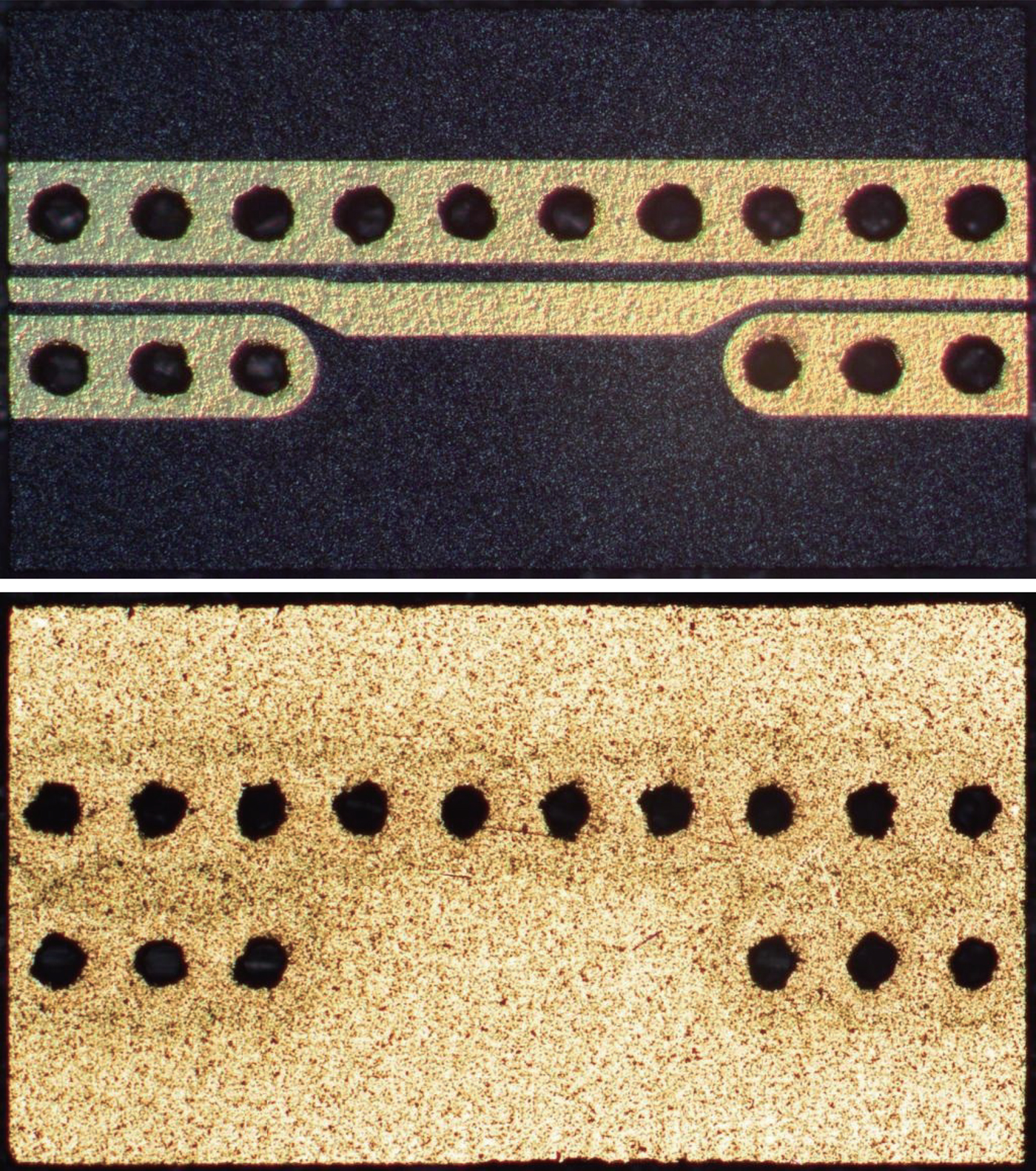
Fig. 8. Fabricated CPW-to-ACPS transition in a back-to-back configuration based on AlN substrate.
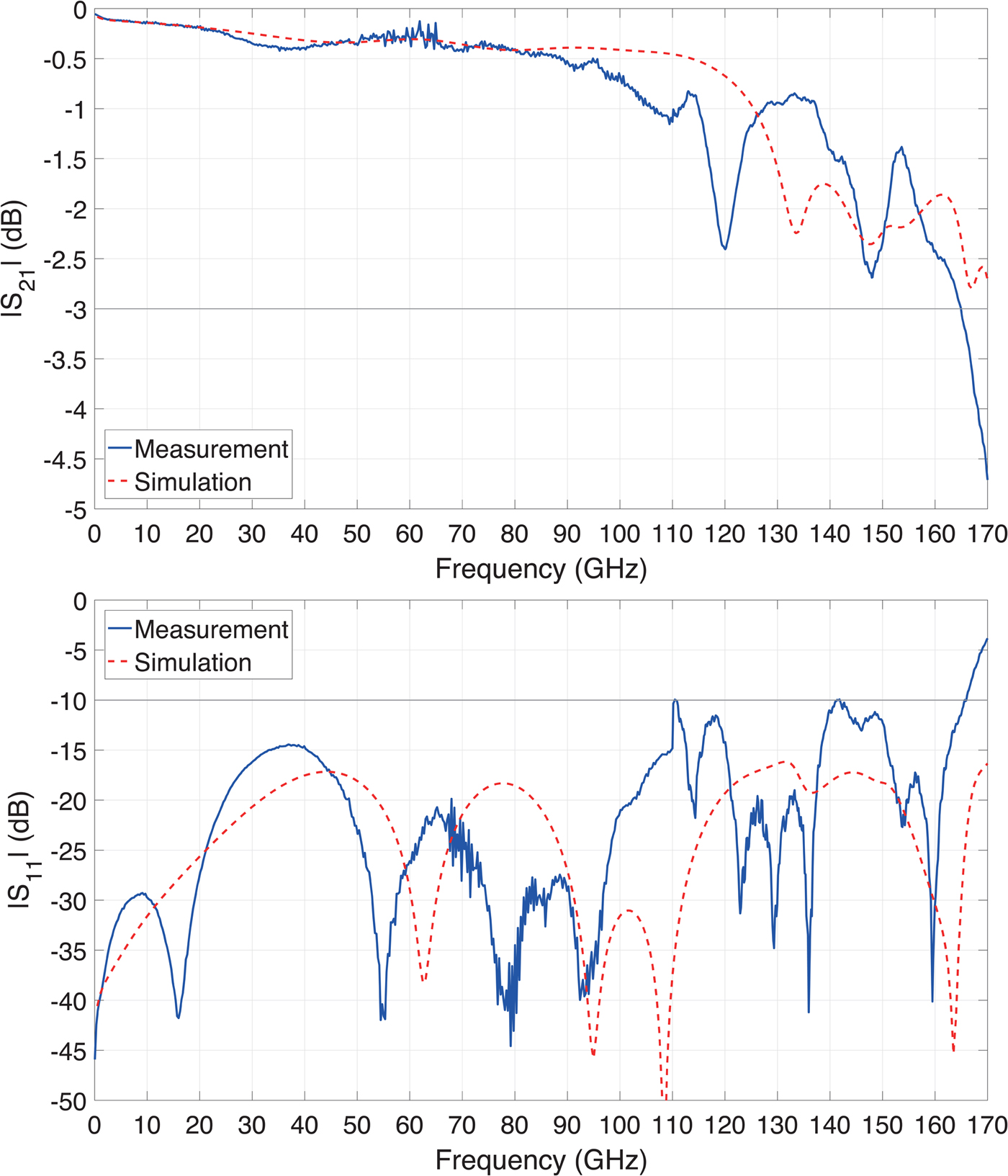
The fabricated CPW-to-ACPS transition was characterized on-wafer using a probe station, a vector network analyzer and two GSG probes with 125 μm pitch. The two-port scattering parameters were firstly measured from DC to 110 GHz and then the setup was reconfigured for on-wafer measurement from 110 to 170 GHz.
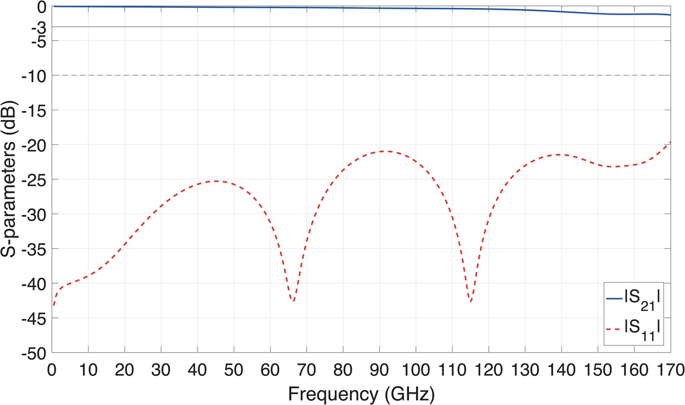
Since the bandwidth of the transition is referred as the width of the frequency band where the return loss is better than 10 dB, the proposed CPW-to-ACPS transition in a back-to-back configuration exhibits a simulated bandwidth of 170 GHz which is shown by the red dashed lines in Fig. 9. From DC to 170 GHz, the simulated insertion loss is <2.8 dB. The blue solid lines in Fig. 9 show the measurement results of the fabricated CPW-to-ACPS transition in a back-to-back configuration. Compared with the simulation results, a reasonable agreement has been achieved. The fabricated CPW-to-ACPS transition in a back-to-back configuration provides a bandwidth of 165 GHz with an associated insertion loss of 3 dB. The differences between simulation and measurement results are mainly caused by the variation of electrical properties based on frequency for the AlN substrate as well as the fabrication tolerances, especially for the surface roughness of the gold conductors and the diameter of the vias. Besides, reconfiguring the measurement setup at high frequencies results in small step discontinuities at 110 GHz on the measured scattering parameters.

Fig. 9. Simulation (red dashed lines) and measurement (blue solid lines) results of the proposed CPW-to-ACPS transition in a back-to-back configuration.
In Table 1, this work is compared with other GSG-to-GS transitions published in the literature. Wire bonding bridges are used in [Reference Anagnostou, Morton, Papapolymerou and Christodoulou18, Reference Dong, Johansen, Zhurbenko and Hanberg28] for increasing the bandwidth and in order to suppress parasitic modes either thick substrate or absorber layer is needed. Though the transition with air-bridge reported in [Reference Kim, Jeong, Lee, Kim, Lim, Seo and Nam29] can achieve a bandwidth of 110 GHz, it requires multilayer patterning process based on thick substrate. In this work, based on the same substrate as used in [Reference Dong, Johansen, Zhurbenko and Hanberg28], a bandwidth of 165 GHz has been achieved by the proposed transition with vias which is more than twice as large as the bandwidth reported in [Reference Dong, Johansen, Zhurbenko and Hanberg28]. While having the largest bandwidth, the proposed CPW-to-ACPS transition is based on thin AlN substrate and it does not require extra structures on the top or absorber layer underneath which also makes the transition more compact and versatile for system integrations.
Table 1. Comparison between this work and published GSG-to-GS transitions
Conclusion
An ultra-wideband CPW-to-ACPS transition with vias based on AlN substrate has been presented in this work. The concepts of designing CPW, ACPS, and CPW-to-ACPS transition were explained. The effect of adding vias through the substrate was also discussed. The CPW and ACPS with vias were designed based on AlN substrate and simulated in HFSS. The designed CPW-to-ACPS transition with vias going through AlN substrate was demonstrated in detail. The proposed CPW-to-ACPS transition with vias was fabricated and measured in a back-to-back configuration. A reasonable agreement has been achieved between simulation and measurement results. The fabricated CPW-to-ACPS transition can provide a bandwidth of 165 GHz with an associated insertion loss of 3 dB. While having the largest bandwidth, the proposed CPW-to-ACPS transition is also more versatile for compact system integrations.
Acknowledgement
The work was supported in part by the EU funded project PANTHER under contract number 619411.
 Yunfeng Dong received the B.Sc. degree in Electronic Information Engineering from the Beijing University of Technology (BJUT), Beijing, China, in 2012, the M.Sc. degree in Wireless Engineering from the Technical University of Denmark (DTU), Lyngby, Denmark, in 2014, and is currently working toward the Ph.D. degree at DTU. From September 2011 to July 2012, he was an exchange student with the South-Eastern Finland University of Applied Sciences (XAMK), Mikkeli, Finland. From October 2014 to December 2014, he was a Research Assistant with the Electromagnetic Systems Group (EMS), DTU, Lyngby, Denmark. From October 2017 to November 2017, he was a visiting scholar with the Terahertz Systems Technology Group, the Technische Universität Darmstadt, Darmstadt, Germany. His current research interests include developing innovative strategies that are suitable for hybrid integration and packaging at millimeter-wave and terahertz frequencies.
 Tom K. Johansen received his M.Sc. and Ph.D. degrees in Electrical Engineering from the Technical University of Denmark (DTU), Lyngby, Denmark, in 1999 and 2003, respectively. In 1999, he joined the Electromagnetic Systems Group (DTU Elektro), DTU, where he is currently an Associate Professor. From September 2001 to March 2002, he was a Visiting Scholar with the Center for Wireless Communication, the University of San Diego, San Diego, CA, USA. From November 2012 to February 2013, he spent a sabbatical with the Ferdinand Braun Institute (FBH), Berlin, Germany. His research interests include the modeling of HBT devices, millimeter-wave and sub-millimeter-wave integrated circuit design, and reconfigurable microwave components.
 Vitaliy Zhurbenko received the M.Sc. degree in Electrical Engineering from the Kharkiv National University of Radio Electronics, Kharkiv, Ukraine, in 2001, and the Ph.D. degree in Electrical Engineering from the Technical University of Denmark (DTU), Lyngby, Denmark, in 2008. In 2005, he joined DTU, where he is currently an Associate Professor. His current research and teaching interests include microwave and millimeter-wave sensing for biomedical and security applications; microwave and millimeter-wave components and integrated circuits for instrumentation applications; antennas and passive circuit design and characterization; and magnetic resonance technology.