


Introduction
The rapidly growing user demand for wireless connectivity has caused Wi-Fi standards to evolve over the last decade. One technique which could theoretically double data capacity is FD by allowing simultaneous transmission and reception (STAR) on the same frequency channel [Reference Laughlin, Beach, Morris and Haine1, Reference Deo, Mirshekar-Syahkal and Zheng2, Reference Nawaz, Niazi, Basit and Shaukat3]. A single antenna FD system [Reference Laughlin, Beach, Morris and Haine1] facilitating STAR is shown in Fig. 1. Single-antenna FD systems require a combining network to couple the transmitted signal from the power amplifier (PA) and the received signal to the antenna. Dual-antenna systems have also been proposed, but the space required for two antennas [Reference Deo, Mirshekar-Syahkal and Zheng2] can often outweigh any advantages. Similarly, single-antenna solutions using dual polarization exist in the literature but are complex in design [Reference Nawaz, Niazi, Basit and Shaukat3] and cannot be used with low-cost off-the-shelf dipole-type antennas as often found in consumer electronics.

Fig. 1. Conceptual FD system.
STAR is hampered by self-interference, where the transmitted signal interferes with the received one. Due to path-loss, the transmitted signal is often 100 dB greater than the received one, at a minimum masking it, but potentially damaging the delicate receiver low-noise amplifier (LNA). Practical combing network will typically only provide 30 dB of isolation between the received and transmitted ports. In addition to this leakage signal, part of the transmitted signal is reflected into the receive path due to antenna mismatch – a significant source of self-interference in FD systems [Reference Wu, Shen and Tang4]. To overcome self-interference, a cancellation network is included between the antenna combiner and the LNA. A portion of the transmitted signal is tapped off, gain and phase manipulated and injected into the receive path to cancel the self-interference. In Fig. 1 there are two levels of cancellation, one in the analogue domain before the LNA and a second one after down-conversion in the digital domain.
Most published FD system level study uses circulators as the combining network [Reference Bharadia, McMilin and Katti5] because they have low (<1 dB) insertion loss but are often too large and expensive for consumer electronics. Transmission line networks like the rat-race coupler [Reference Wagner, Stelzer and Jager6], hybrid coupler [Reference Laughlin, Beach, Morris and Haine1] and directional coupler [Reference Zhang, Zhou and Qian7] provide a more practical solution.
This study integrates a combining network based on a rat-race coupler with the analogue cancellation network. To do this, the rat race must be made tuneable. Tuneable rat-race couplers have previously been proposed in the literature either by loading transmission lines with varactor diodes [Reference Lin and Ma8, Reference Tan and Lin9], or incorporating piezo activator tuned cavities [Reference Hagag and Peroulis10]. The tuneable rat race proposed here substitutes its fourth port for a variable attenuator and phase-shifter in one of the arms, therefore facilitating tuning. This not only tunes the rat-race's inherent isolation, but also compensates for the antenna mismatch.
Although the focus of this study is Wi-Fi communications in the ISM band, it can be applied to other applications: frequency-division-duplexing [Reference Nightingale11], radar [Reference Wagner, Stelzer and Jager6] and test and measurement [Reference Venere, Hurtado, La Valle and Muravchik12].
Prior related study by the author is described in Reference [Reference Watkins, Thompson and Halls13] which although also intended for Wi-Fi, used a different architecture. That was based around a hybrid coupler with its fourth port terminated in a variable impedance (Z V) as shown in Fig. 2(b). Z V consisted of a digitally controlled switched attenuator and a digitally controlled switched phase shifter. These were connected in series with the other end of the attenuator terminated in a short circuit. The reflection – and hence impedance – seen looking into the phase shifter could be controlled in magnitude by the attenuator and phase by the phase shifter.
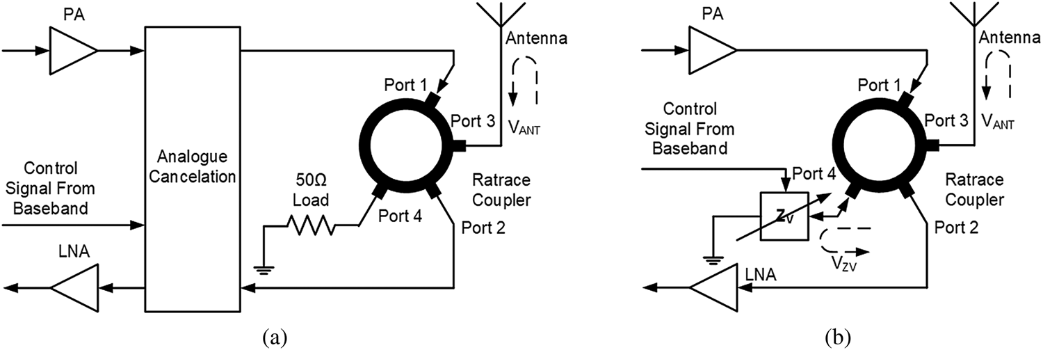
Fig. 2. FD architecture with rat-race coupler; (a) separate analogue cancellation and rat race, (b) rat race with variable impedance.
Rat-race full duplex coupler
The frontend of a single-antenna rat-race full duplex (FD) system is shown in Fig. 2(a). The communications system baseband circuitry generates a modulated RF signal from an input data source which is amplified by the PA. This signal is applied to port 1 of the rat-race coupler. Port 2 of the rat race is connected to the LNA in the receive path. An antenna is connected to port 3 and a 50 Ω load to port 4. The reflected portion of the transmitted signal due to antenna mismatch is represented by vector V ANT. In an ideal rat-race coupler, there is a 180° phase difference between the two paths between ports 1 and 2. This phase difference leads to anti-phase cancellation of the transmitted signal at port 2, if V ANT is zero. Including V ANT adds a further interference component which an ideal rat race cannot cancel, which is why an analogue cancelation block is required. In addition to the simplified schematics of Fig. 1, a control signal generated by the baseband is required to control the analogue cancellation block for maximum self-interference cancellation (SiC).
One combined analogue cancellation and coupler solution proposed in the literature is to use a hybrid coupler with its fourth port terminated with a Z V which can inject a voltage (V ZV) to cancel V ANT [Reference Watkins, Thompson and Halls13] and any residual self-interference due to leakage from the hybrid. This can similarly be applied to a rat race as shown in Fig. 2(b) where Z V is connected to port 4. Z V is controlled by the baseband so that V ZV cancels V ANT at the input of the LNA, therefore increasing SiC.
The classic rat-race [Reference Ho, Hong and Li14] coupler shown in Fig. 2 is composed of six transmission line sections as expanded in Fig. 3(a). Each transmission line is a quarter wavelength (λ/4) long with an impedance of √2 times the system impedance (50 Ω here, resulting in 70.7 Ω). Between ports 1 and 2 one path passes through TL2,3 and the other through TL1,4–6. The signal passing through TL1,4–6 is described as V ISO. It can be found in Cadence's Microwave Office (MWO) simulation that if an input current i IN flows into port 1, a current with a half its magnitude and phase shifted by 180° flows out of TL3 into port 2. However, a current with the same magnitude but in-phase with i IN flows out of TL4 into port 2. The two currents cancel resulting in close to zero volts at port 2. A small voltage divided by large current results is equivalent to a low impedance. Because all the TLs are 90°, they operate as quarter wavelength transformers, resulting in a high impedance at their other end, and hence little current flow.
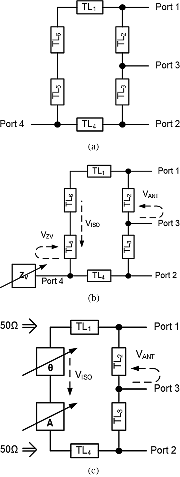
Fig. 3. Rat race-based FD frontend where all TLs are 70.7 Ω unless indicated otherwise: (a) conventional rat-race coupler, (b) rat-race coupler with Z V and (c) modified rat-race coupler where the characteristic impedance of A and θ is 50 Ω.
In Fig. 3(b) Z V is connected to port 4, such that part of V ISO is reflected back into the rat race as V ZV. The gain and phase of V ZV relative to V ISO is controlled by Z V. Z V can be produced by several means, but most common are those involving variable gain and phase control elements [Reference Watkins, Thompson and Halls13], although other techniques also exist for achieving this.
A further observation is that the voltage present and current flowing out of the TL1 into TL6 has a ratio of 50 – an impedance of 50 Ω. A similar relationship is found to TL5. Reducing the impedance of TL5 and TL6 to 50 Ω allows the coupler to still balance and port 2 to be isolated from port 1. This opens the potential to tune the isolation by controlling the TLs. In this study, Z V is removed and a variable attenuator (A) and variable phase shifter (θ) substituted for TL5 and TL6 in the V ISO path as shown in Fig. 3(c). To ensure the correct cancelling at port 2, the electrical length of A and θ should be centered around half a wavelength. From simulation the optimum value for A was found experimentally to be approximately 3 dB when port 3 is terminated in a 50 Ω load. This value for A will be different when port 3 is terminated with an antenna, as that will introduce V ANT, which is not present with a perfect 50 Ω simulated load. It was also noted in the simulation that this 3 dB value is dependent on impedance of the transmission lines, any deviation from the theoretical 70.7 Ω resulted in a different optimum attenuation.
To understand the operation of the modified rat-race coupler the scattering matrix of a conventional coupler is shown in Equation (1). It is important to note that the arrangement of the scattering matrix will depend on the labelling of the ports. (1) Refers to Fig. 3(a) where a signal entering a port experiences an equal power split (3 dB) and 90° phase shift as it passes through a transmission line section to its adjacent port. Those paths where the signal is cancelled (S 12/S 21 and S 34/S 43) are zero.

With A and θ optimally adjusted, the three-port coupler shown in Fig. 3(c) and expressed in Equation (2) has an insertion loss of 3 dB and 90° phase shift for S 31 and S 32. S 21 will be zero due to cancellation. The layout in Fig. 3(c) has a similar structure to a Wilkinson power splitter in that it is also a three-port device and dissipates power in a resistive element. In this respect, TL1, TL4, A and θ replace the resistive element between the two output ports.

The 3 dB insertion loss through each path experienced in Equation (2) will have an adverse impact on system performance. In the transmitter path the output power will be halved. Because the DC power unchanged the PA, its efficiency will also be halved. Similarly, 3 dB insertion loss in the receiver path will increase the noise figure by 3 dB as the coupler is the first element in the receiver chain. This is a known issue with many proposed FD architectures [Reference Laughlin, Beach, Morris and Haine1]. The only currently known alternative are circulators [Reference Bharadia, McMilin and Katti5] which as stated above have <1 dB insertion loss but are physically large and so unsuitable for consumer electronics.
Gain and phase balance
To determine the level of possible SiC, the individual elements of the combined analogue canceller and combining network must be evaluated. As previously mentioned, the antenna suffers from mismatch resulting in the self-interference component V ANT. V ANT can be a significant source of self-interference as determined by measuring three practical sleeve-dipole antennas – as often used by ISM band 2.45 GHz Wi-Fi routers. The antennas were: (A) RF Solutions ANT-24G, (B) L-COM HG2403RD and (C) Siretta Delta 6B. The results for antennas (A)–(C) are shown in Fig. 4 where the return loss can be as good as −33 dB, or as bad as −13 dB depending on the antenna and frequency.

Fig. 4. Measured return loss of three off-the-shelf sleeve dipole 2.45 GHz ISM band Wi-Fi antennas.
Assuming an ideal rat-race coupler, then the self-interference is solely dependent on the antenna return loss. V ZV role is then to improve the SiC beyond that provided by the antenna. Achieving a large degree of SiC is only possible if the V ZV and V ANT have identical amplitude and are exactly in antiphase when arriving at the LNA input. The SiC for a given gain (δA) error and phase error (δθ) can be determined using Equation (3) [Reference Kenington15]:

From Equation (1), Fig. 5 is derived where to achieve say 60 dB of SiC in the rat-race coupler, on top of that produced by the antenna, the gain and phase error need to be better than 0.01 dB and 0.01°, respectively. Assuming this was possible, and antenna C was used at 2.45 GHz, 91 dB could be achieved. This requires that the tuning resolution of A and θ be in the order of 0.01 dB and 0.01°. This level of SiC is only maintained over the bandwidth where the gain and phase error remain within these limits. This becomes a challenge if the impedance of the antenna (and hence the magnitude and phase of V ANT) changes significantly over its operating band as does that of Z V. The rat-race isolation will also be reduced, as the relative wavelength of the TLs move away from a quarter wavelength as frequency changes, resulting in a narrowband response.

Fig. 5. Gain and phase error impact on SiC.
The resolution and range requirements of A and θ are not currently available with digital switched control elements, so analogue must be used. One challenge for A and θ is that they must have a low insertion loss, approximately 3 dB as described in section “Rat-race full duplex coupler”. Therefore it should have a minimum loss of less than 3 dB. A common configuration are hybrid coupler-based reflection variable attenuators and phase shifters [Reference Kenington15]. Theoretically these have minimum loss, but when simulated with practical components often have excess insertion loss greater than 3 dB. To minimize the loss, for this work A is a Π type attenuator incorporating a PIN diode in the series element with two fixed shunt resistors and θ is hybrid coupler reflection phase shifter incorporating varactor diodes as shown in Fig. 6.

Fig. 6. Analogue attenuator and phase shifter.
A Π attenuator is chosen as the series element can be replaced with a PIN diode. A PIN diode will have a low RF resistance when DC current passes through it. To complete the attenuator two 1 kΩ shunt resistors are included. A PIN diode resistance of 3 Ω corresponds to 0.7 dB attenuation and 100 Ω 5.7 dB. A BAP50-04W was selected for this, which corresponds to a DC current of 100 μA to 10 mA.
The hybrid coupler phase shifter was chosen as although it incurs a moderate insertion loss, it is capable of a large phase tuning range and the insertion loss does not change much over the tuning range. The insertion loss is attributed to the series resistance of the varactor diodes. BB837 diodes were selected which have a series resistance of 1.5 Ω. The BB837 has a capacitance range of 0.5–6.6 pF corresponding to a reverse voltage 1–28 V. For the MWO simulation the varactor diodes were BB837 and the PIN diode a BAP50-04W. These were chosen due to their availability at the time. When incorporated in the schematic of Fig. 6 with 1 kΩ shunt resistors for A, the gain and phase response were simulated as shown in Fig. 7 where an enclosed area is defined for 2.4, 2.45 and 2.5 GHz. Figure 7 shows that there is a degree of dependency between A and θ due to stray parasitic components. In particular, the shunt capacitance of the PIN diode introduces a phase shift at high attenuation setting where it becomes the dominant path.

Fig. 7. Tuning area of Fig. 6, where sold black line is 2.4 GHz, small dashes are 2.45 GHz and big dashes are 2.5 GHz.
Simulated results
A full simulation of the rat-race frontend including the models for the varactor and PIN diodes was developed. It was first simulated with a 50 Ω load on the antenna port (port 2) of the rat-race coupler. A and θ were manipulated to produce a high level of isolation for the combined rat race and analogue cancellation over the whole 2.45 GHz ISM band. The results for this are shown in Fig. 8 where it can be shown that greater than −65 dB narrowband isolation can be tuned over the whole ISM band.

Fig. 8. Simulated isolation between ports 1 and 2 for different θ and A settings with 50 Ω load.
During these simulations, the S 31 and S 32 – effectively the insertion loss – of the rat-race coupler were flat across the whole band for a given combination of A and θ. Tuning A and θ to tune the SiC null did result in a variation of S 31 and S 32 between 3.6 and 3.8 dB. This is higher than the theoretical 3 dB for the rat-race coupler due to substrate losses – the simulations were carried out on a realistic FR4 substrate or mismatch between the TLs. Worst return loss from any port under these conditions was −14.6 dB. The optimum attenuation and phase settings were recorded while tuning and displayed in Fig. 9, where the attenuation setting is flat at −3.52 dB and the phase varies by 3.3° between 217.4° and 220.7°.

Fig. 9. Simulated θ and A settings for maximum isolation with 50 Ω load.
The measured S-parameters of the three Wi-Fi sleeve-dipole antenna shown in Fig. 4 were then incorporated into the simulation as a sub-circuit connected to port 2. Antenna C was found to be the best. Its simulated results are presented in Fig. 10 where better than −57 dB narrowband SiC between ports 1 and 3 could be achieved over the whole 2.45 GHz band.

Fig. 10. Simulated SiC between ports 1 and 2 for different θ and A settings with measured antenna C as load.
With the measured antenna C included in the simulation, the worst return loss from the ports 1 and 2 (S 11 and S 22) was −14.7 dB. The optimum A and θ settings are displayed in Fig. 11, where they can be seen to vary more than when port 3 was terminated with a 50 Ω load. A varies by 1.8 dB between −3.7 and 5.5 dB, θ by 15.4° between 208.7° and 224.1° for optimum SiC. This is to be expected as antenna C mismatch varies considerably over the band as shown in Fig. 4.

Fig. 11. Simulated θ and A settings for maximum isolation with antenna C as load.
Measured results
To verify further the operation of the tuneable rat-race frontend, a prototype was constructed on an FR4 substrate for use at 2.45 GHz as shown in Fig. 12. Measurements were taken on a Rhode and Schwarz ZNB20 vector network analyser (VNA) and are shown in Fig. 13 with antenna C connected. Better than −58 dB narrowband SiC could be achieved over the whole band. It should be noted that these results were not taken in an anechoic chamber, but in a typical laboratory space where there were reflections from the walls, metal enclosed equipment and the researcher taking the measurements. These results show a higher isolation than other published tuneable rat-race couplers [Reference Zhang, Zhou and Qian7, Reference Lin and Ma8, Reference Tan and Lin9]. However, those results were taken with a 50 Ω load at port 2, whereas these are with the commercial sleeve dipole, so are not completely comparable, but do justify the value of this simpler tuneable rat-race implementation.

Fig. 12. Photograph of prototype: input port is on the left, antenna port at the top, output port on the right the A and θ controlled by multiturn variable resistors on the bottom and on the middle of the board on the left is a shortened quarter wavelength stub for DC return.

Fig. 13. Measured SiC between ports 1 and 2 for different θ and A settings with antenna C.
The optimum values for A and θ for Fig. 13 are shown in Fig. 14. They are shown to vary considerably more than the simulated results presented in Fig. 11. This is likely due to fabrication tolerances as acceptable gain and phase errors are very small for a large SiC, as shown in Fig. 5. The values in Fig. 13 were derived by measuring the tuning voltages for both A and θ at the middle terminals of the two multiturn variable resistors shown at the bottom of Fig. 12. Using the datasheets for the BAP50-04W and the BB837, along with the schematic in Fig. 6, the corresponding A and θ values were calculated and plotted in Fig. 14.

Fig. 14. Measured θ and A settings for maximum isolation with antenna C.
The rat-race frontend was further evaluated by injecting a standard compliant 20 MHz Wi-Fi signal as would be used in a commercial FD system into the input port and monitoring the output port. The Wi-Fi signal was generated by a Keysight N5172B EXG Signal Generator with a Keysight N9010A EXA Signal Analyzer as the receiver. A and θ were tuned for maximum SiC over the whole 20 MHz bandwidth of the Wi-Fi signal. An example result is shown in Fig. 15 at 2.45 GHz, where both the transmitted and received signal (at port 2) are shown. Under these conditions −42 dB of average SiC was achieved over the 20 MHz signal bandwidth relative to the transmitted signal. In this measurement, the RF signal generator was set to 10 dBm, resulting in a total power of 6.3 dBm over the signal bandwidth.

Fig. 15. Measured spectrum with 20 MHz Wi-Fi signal: the transmitted signal, SiC with the tuneable rat race and a comparison with an off-the-shelf circulator.
For comparison, the performance of a Cerncx off-the-shelf circulator is included intended for 2.5–2.55 GHz operation. When the circulator is terminated with a 50 Ω load −42 dB of average SiC was achieved at 2.45 GHz comparable to the rat-race coupler. However, when the load was replaced with antenna C, the SiC degraded to −16 dB due to antenna mismatch. This justifies the use of a tuneable rat-race coupler as any network must adapt to a practical antenna.
Similar results were achieved over all regions of the band. The SiC contains a null mirroring the narrowband responses of Fig. 13. This level of SiC and simplicity of its design verifies the feasibility of a rat-race frontend for FD. When combined with digital cancellation, an overall system should be capable of a high level of performance to achieve the intended FD communications.
Fig. 16 shows the port response as measured on the VNA with the SiC tuned to 2.45 GHz as shown by the S 21 response. The S 11 and the S 22 are the two return losses from ports 1 and 2, respectively. At 2.45 GHz, S 11 is −9.3 dB and S 22 −26.7 dB indicating a good level of match. The match is dependant on the settings of A and θ, so needs to be considered to ensure that the PA and LNA of the FD system are not subjected to a high standing wave ratio (SWR) which could lead to instability.

Fig. 16. Measured port response when tuned to 2.45 GHz.
Conclusion
This paper describes an RF FD frontend based on a novel tuneable rat-race coupler for the 2.45 GHz ISM band. This is made possible by incorporating analogue control elements into one of the rat-race arms. Under simulation conditions a null of −65 dB could be tuned across the band with a 50 Ω load on the antenna port. Similarly, when the S-parameters for a typical Wi-Fi antenna were incorporated in the simulation, better than −57 dB could be tuned over the whole band.
A practical demonstrator was constructed which produced a −58 dB narrowband SiC null that could be tuned over the whole of the ISM band. To fully evaluate its suitability for FD, a 20 MHz Wi-Fi signal was applied where −42 dB average SiC was achieved at 2.45 GHz over the total bandwidth of the Wi-Fi signal. A similar level of performance was possible over the whole ISM band with this simple architecture.
Acknowledgements
The author thanks all at Toshiba's Bristol Research and Innovation Laboratory for their support in this study.
 G. T. Watkins is a member of both the Institute of Engineering Technology (IET) and the European Microwave Association. He received the MEng degree in electrical and electronic engineering in 2000 from the University of Bristol and a Ph.D. from the same institution in 2003 on the topic of Wideband Feedforward Amplifiers for Software defined Radios.
In 2008 he joined Toshiba Research Europe Limited where he is currently the lead for the Analogue and Digital Systems Programme. He is also the vice chair for the IET RF and Microwave Technical Network and is a regular IET and IEEE reviewer. He is the recipient of a Toshiba Innovation Award for his study on high efficiency FM broadcast transmitters, also the 2015 Best Paper Award from the Internationals Journal of Microwave and Wireless Technology and the 2019 IET Premium Award.
His research interests include: linear power amplifiers, high efficiency system architectures, radar, analogue circuitry, active gate drivers for power electronics, device characterization, 3D printing for RF and Full Duplex communications systems.


