I. INTRODUCTION
During the recent years, the popularity of the modern portable wireless devices such as mobile phones, notebooks, and tablet PCs have drastically increased. These devices not only offer versatility and mobility to the end-user, but also allow multi-GB/s wireless data-transmission for real-time voice and video applications [Reference Wells1]. The feasibility of such devices requires the use of a single-antenna element, which can provide multi-band operation, hence reducing the need of multiple antennas for each of the operating frequency bands [Reference Wells1–Reference Christodoulou, Tawk, Lane and Erwin4]. Such requirements have lead researchers to explore some of the novel multi-band antenna designs [Reference Maci and Gentili2–Reference Zulkifli, Halim and Rahardjo12].
In many applications such as mobile radios, satellites, and wireless communication where weight, cost, ease of installation, and size are constraints, low-profile planar antennas are preferred to fulfill the requirement, which include microstrip patch antennas (MPAs) [Reference Wong, Luk, Chan, Xue, So and Lai3, Reference Christodoulou, Tawk, Lane and Erwin4, Reference Costantine, Kabalan, EI-Hajj and Rammal10, Reference Balanis13]. An MPA typically resonates only at one single frequency. Although there are several other techniques available where an antenna can be made to resonate at multiple frequencies by introducing different shapes of slots [Reference Ali and Khawaja6, Reference Ali, Khawaja, Tarar and Mustaqim7, Reference Lee, Shing and Kishk11, Reference Zulkifli, Halim and Rahardjo12, Reference Razzaqi, Mustaqim and Khawaja14, Reference Kulkarni, Mulgi and Satnoor15] and slits [Reference Zhang and Yang16, Reference Notis, Liakou and Chrissoulidis17] into the main patch.
This paper aims at designing an antenna for WiMax and satellite-based applications. The antenna design presented here shows the use of two slits [Reference Zhang and Yang16] which makes the main patch to resonate at multiple frequency bands. The slits can be realized easily on the metal patch during the fabrication process or with the help of a sharp knife once the antenna is fabricated [Reference Zhang and Yang16]. Most of the antenna features, including radiation pattern and input-impedance remain unaffected by the insertion of the slits. The desired substrate for the MPA design should be thick with low dielectric constant ε r, because they provide large bandwidth and better efficiency at the expense of large size [Reference Maci and Gentili2, Reference Balanis13]. The geometry of the single-element triple-band antenna is shown in Fig. 1 below. The main patch of the antenna has width W and length L. The substrate used is FR4 epoxy glass with thickness h = 1.66 mm and ε r of 4.2.

Fig. 1. Geometry of proposed triple-band MPA.
The relative ε r of the substrate varies typically between 3.8 and 4.7 and dielectric loss tangent tan δ varies from 0.01 to 0.03 in the microwave frequency bands [Reference Kanth, Liljeberg, Tenhunen, Chen, Zheng and Kumar18]. It can be seen from Fig. 1 that, in the proposed MPA design, the 50 Ω microstrip transmission-line feeding technique is used with length L f and width W f. A quarter-wave (QW) transformer of length L t and width W t is also used for the impedance matching between the resonating patch and the feed-line. The slits made at the corner edges of the main patch are of length L s and width W s.
This paper initially presents a single-element MPA design to achieve triple-band behavior using slits with a special focus on mathematical design procedure. For the proof-of-concept, the single-element MPA is fabricated using FR4 substrate to give a comparison between the numerical simulations and the experimental results. Then, a triple-band MPA array design is presented in both 1 × 2 and 1 × 4 configurations. The simulations of the proposed triple-band MPA are performed in Agilent advanced design system (ADS) momentum, an electromagnetic simulator. Its simulation tool is based upon full-wave method of moment (MoM) numerical technique [Reference Balanis13, Reference Kraus and Marhefka19]. The structure of the paper is as follows: Initially, the design procedure of the single-element MPA is discussed in Section II. Section III discusses the simulation and fabricated antenna characterization results and parametric studies on the single-element MPA. Then, triple-band antenna array design and results are presented in Section IV. Finally, Section V draws conclusions.
II. SINGLE-ELEMENT ANTENNA DESIGN
A) MPA design and edge impedance
This section presents the design of the MPA where initially the main patch of the antenna is designed at 3.6 GHz using the basic patch calculations [Reference Balanis13]. The length L, width W, and related parameters of the antenna are calculated using equations (1)–(5):
 $$L\; = \; L_{eff} - 2\Delta L\comma \;$$
where
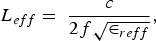 $$L_{eff} = \; \displaystyle{c \over {2f\sqrt { \in _{reff} } }}\comma \;$$
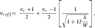 $$\in _{reff} = \; \displaystyle{{ \in _r + 1} \over 2} + \displaystyle{{ \in _r - 1} \over 2}\left[{\displaystyle{1 \over {\sqrt {1 + 12\displaystyle{h \over W}} }}} \right]\comma \;$$
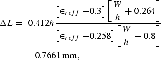 $$\eqalign{\Delta L &= \; 0.412h\displaystyle{{\left[{ \in _{reff} + 0.3} \right]\left[{\displaystyle{W \over h} + 0.264} \right]} \over {\left[{ \in _{reff} - 0.258} \right]\left[{\displaystyle{W \over h} + 0.8} \right]}}\; \cr & \quad = 0.7661\, {\rm mm\comma \; }}$$
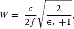 $$W = \; \displaystyle{c \over {2f}}\sqrt {\displaystyle{2 \over { \in _r + 1}}}\comma \;$$
where L eff is the resonating length of the patch and ∈reff is the effective dielectric constant due to fringing effect.
The edge impedance of the MPA is calculated using the transmission-line model [Reference Balanis13], where the patch of an antenna is equivalent to two radiating slots. In general, the input-impedance calculations of the patch result in the complex impedance. According to [Reference Balanis13] if an antenna resonates at (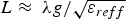 $L \approx \; \lambda g/\sqrt {\varepsilon _{reff} } $), then the total admittance of the antenna becomes real and in turn the impedance at the edges of the antenna become real as well which is calculated by the formulas described in equation (6)–(10):
 $$R_{in} \left({x_0 = 0} \right)= \displaystyle{1 \over {2\lpar G_1 + G_{12} \rpar }}\comma \;$$
where
 $$G_1 = \displaystyle{{I_1 } \over {120\pi ^2 }}\comma \;$$
 $$I_1 = \mathop \int \limits_0^\pi \left[{\displaystyle{{{\rm sin}\left({\displaystyle{{k_0\, W} \over 2}{\rm cos}\theta } \right)} \over {{\rm cos}\theta }}} \right]^2 {\rm sin}^3 \theta d\theta\comma \;$$
 $$k_0 = \displaystyle{{2\pi } \over {\lambda _0 }}\comma \;$$
 $$G_{12} = \displaystyle{1 \over {120\pi ^2 }}\mathop \int \limits_0^\pi \left[{\displaystyle{{{\rm sin}\left({\displaystyle{{k_0\, W} \over 2}{\rm cos}\theta } \right)} \over {{\rm cos}\theta }}} \right]^2\, J_0 \left({k_0\, L{\rm sin}\theta } \right){\rm sin}^3 \theta \, d\theta\comma \;$$
where R in(x 0 = 0) refers to the impedance at the slit edge in the main patch, G 1 is the conductance of one radiating slit, as shown in Fig. 1, and G 12 is the mutual conductance between the radiating slits. In equation (10), J 0 and θ are Bessel function and directivity, respectively. The above formulas give a high edge impedance of 311 Ω. This edge impedance can be further optimized using equation (11) below for this type of antenna [Reference Kraus and Marhefka19]:
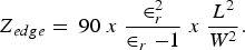 $$Z_{edge} = \; 90\; x\; \displaystyle{{ \in _r^2 } \over { \in _r - 1}}\; x\; \displaystyle{{L^2 } \over {W^2 }}.$$
From the above equation, the optimized edge impedance is calculated to be 273 Ω. It can be seen from Section III below, that the better performance is achieved when edge impedance value of 273 Ω was used for the design of matching network.
B) Matching network
A QW transformer [Reference David20] can be used to match the patch antenna input-impedance at resonance with a 50 Ω transmission-line. A similar technique is used in this design, where a QW transformer, i.e. transmission-line of length λ/4 is used which changes the input- impedance of the load to another value, so that the matching is possible. The impedance of the QW transformer is calculated using equation (12) below:
 $$Z_t = \sqrt {Z_o Z_L }\comma \; $$
where Z o and Z L are input impedances, which are required to be real in order to perform the matching. If Z L is complex, then it can be made real by adding a small transmission-line, i.e. stub matching can be used [Reference David20]. If the input-impedance of the antenna is real as in our case, then QW transformer can be used directly without the need of any matching stub.
C) Slits
A single resonant frequency (f r) operation MPA can be modified to resonate at multiple frequencies by adding different shapes of slits and slots [Reference Ali and Khawaja6, Reference Ali, Khawaja, Tarar and Mustaqim7, Reference Lee, Shing and Kishk11, Reference Zulkifli, Halim and Rahardjo12, Reference Razzaqi, Mustaqim and Khawaja14–Reference Notis, Liakou and Chrissoulidis17] on the main patch. The slots can be of various types which include mainly C, E, F, and U-shaped, each one with its own effects and properties. But, for the proposed antenna design, two symmetrical slits are used which are placed at the edges of the triple-band MPA, as depicted in Figs 1 and 2. The addition of slits makes the MPA tunable, without affecting any other features of the antenna. It can also be observed in the later sections that the designed QW transformer remained the same even after the inclusion of slits on the main patch [Reference Notis, Liakou and Chrissoulidis17]. The optimized dimensions of slits with L s = 8 mm and W s = 2 mm were obtained by initially cutting a small portion on the main patch. Then, the length of slit was increased gradually until the desired frequency bands were obtained. The effect of variation of slit dimension on the antenna f r is observed and studied in the next section. The summary of triple-band MPA design parameters are summarized in Table 1 below.
Fig. 2. Fabricated single-element triple-band MPA.
Table 1. Triple-band antenna dimensions.
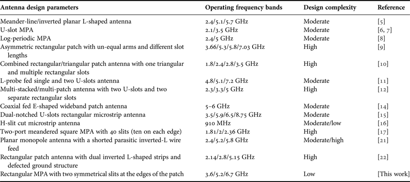
A number of researchers [Reference Maci and Gentili2, Reference Christodoulou, Tawk, Lane and Erwin4–Reference Zulkifli, Halim and Rahardjo12, Reference Razzaqi, Mustaqim and Khawaja14–Reference Notis, Liakou and Chrissoulidis17, Reference Jan and Tseng21, Reference Liu, Wu and Dai22] have proposed different design techniques and methods that can make a single-element antenna to operate at multiple frequency bands. In most cases, the antenna size is large and the geometry of the antenna is complicated. In some cases, although the antenna is compact, it shows a quite high level of cross-polarization. Table 2 gives a detailed summary of the previous multi-band antenna designs proposed in the literature and compare it with the work presented in this paper in terms of antenna design complexity and frequency bands of operation.
Table 2. Comparison of multi-band antenna design techniques.
It can be observed from Table 2 that most of the proposed designs techniques for multi-band antenna have high complexity as compare to the design proposed in this work which makes it a more attractive solution for multi-band antenna design.
III. SINGLE-ELEMENT ANTENNA MODELING AND CHARACTERIZATION RESULTS
The designed triple-band MPA is simulated in ADS momentum. The MPA has two symmetrical slits at the corner edges for providing multi-band operation. A QW transformer-matching technique is employed with a transmission-line feed to match the characteristic impedance of the 50 Ω port with the MPA. The designed antenna is then fabricated using the FR4 substrate and is shown in Fig. 2. The dimensions of the single-element triple-band MPA are summarized in Table 1.
The reflection coefficient (S 11) measurements of the antenna were performed using Agilent PNA N5230A. The comparison of the simulated and measured S 11 plots of the single-element antenna is shown in Fig. 3. It can be seen from Fig. 3 that there are three main resonance frequencies achieved.
Fig. 3. Simulated and measured S 11 plots of single-element triple-band MPA.
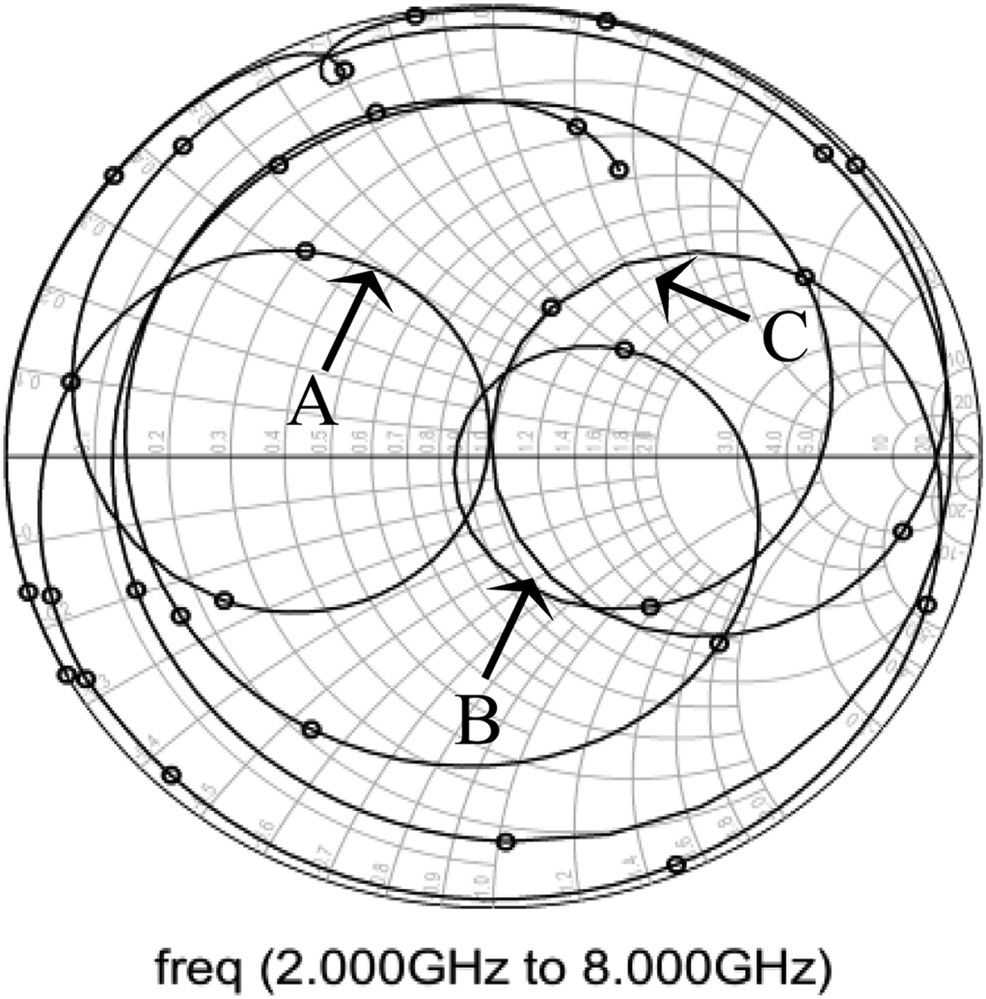
The simulated/measured S 11 values about 3.6, 5.2, and 6.7 GHz are −34/ − 16.4 dB, −18.8/ − 15 dB, and −21.5/ − 17 dB, respectively. These values suggest that the MPA has good impedance-matching as desired. Same results are shown in Fig. 4 using the smith-chart. Different circles of S 11 at different frequencies can be seen in Fig. 4 and it is important to note that there are three circles (marked as A, B, and C), which are very close to the middle matching point with a real value of 1 on the smith-chart.
Fig. 4. Smith chart showing S 11 circles at different frequencies.
The 10 dB impedance bandwidth achieved for simulated/measured triple-band MPA is 57/80 MHz, 56/79 MHz and 184/210 MHz about 3.6, 5.2, and 6.7 GHz, respectively. It is important to observe that better performance in terms of improved impedance bandwidth is achieved for the fabricated triple-band MPA.
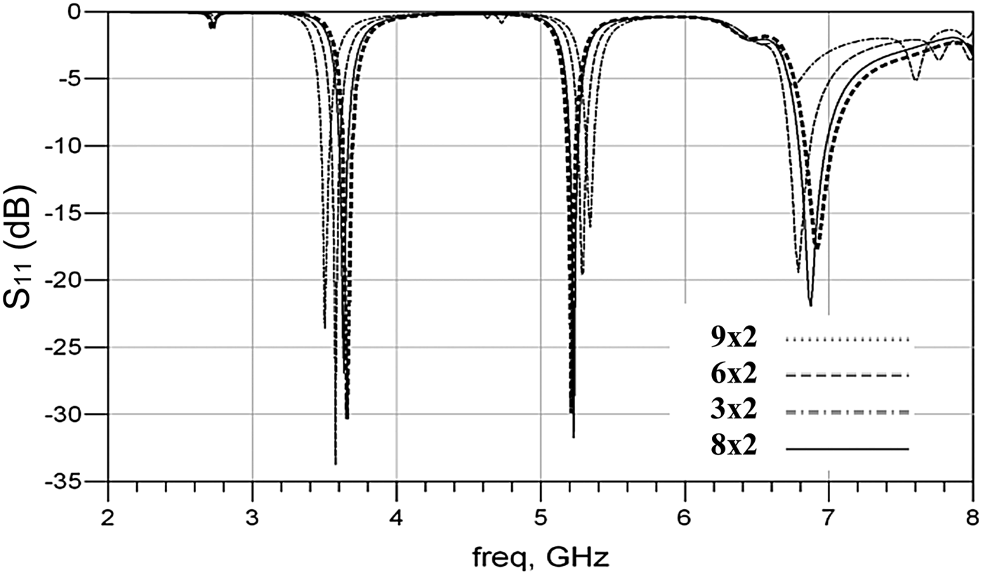
The effect of change of slit dimension on the MPA performance is then studied. Different slit dimensions are tried during the antenna design by varying the L s and keeping the W s parameters as constant. It can be seen from Fig. 5, that the most optimized results in terms of S 11 are obtained, when the slits have the dimensions of 8 × 2 mm, shown by a solid line in Fig. 5. This parametric study suggests that triple-band MPA behavior can be tuned by carefully choosing the slits dimensions. Another interesting behavior that is observed during the parametric study is the tuning of the high-frequency resonance about 6.7 GHz. This is achieved by varying the length of upper slit and keeping the dimensions of lower slit fixed at 8 × 2 mm.
Fig. 5. Effect of the change of upper and lower slit-lengths (L s) on S 11.
The results are shown in Fig. 6 and it can be seen that as the L s in the upper slit is increased from 8 to 13 mm, the 6.7 GHz resonant frequency starts to drift toward the 7 GHz band and above. Another important behavior to observe in Fig. 6 is that there is no change in the other f r, although the S 11 response at 3.6 GHz is changed from −27 to −50 dB.

Fig. 6. Effect of variation in upper slit dimensions on S 11.
The current distribution of the triple-band MPA is demonstrated in Fig. 7. It can be seen that at higher frequencies, the two slits of the antenna are also radiating. This confirms that by inserting slits on the patch and by carefully selecting appropriate position for the slits, current disturbance can be caused which in turn triggers another radiation as highlighted in Fig. 7.
Fig. 7. Surface current distribution of the triple-band MPA.
The radiation patterns for the simulated antenna are plotted using ADS momentum visualization tool and measurements of the fabricated antenna are made in RF anechoic chamber NI-800F with Agilent N5230A. Figures 8(a)–8(f) show both the simulated and measured two-dimensional (2D) radiation patterns of the antenna at 3.6, 5.2, and 6.7 GHz bands, respectively.
Fig. 8. Single element triple-band MPA simulated (a-c) and measured (d-f) radiation patterns at 3.6 GHz (a, d), 5.2 GHz (b, e) and 6.7 GHz (c, f) respectively.
The given patterns are the horizontal cut of the three-dimensional (3D) radiation pattern at φ = 0° and θ = 0°–360° with finite ground plane considered in simulations, resulting in some back lobes in the radiation patterns as highlighted in Figs 8(a)–8(c). The measured radiation patterns shown are at the same horizontal cut. The designed triple-band MPA has the gain/efficiency characteristic of 7.8 dBi/94.5%, 7.6 dBi/94%, and 7.3 dBi/88% at 3.6, 5.2, and 6.7 GHz, respectively.
These values suggest that the designed multiband MPA operates well at all three resonant frequencies.
IV. ANTENNA ARRAY DESIGN AND RESULTS
After designing the single-element triple-band MPA, a 1 × 2 and 1 × 4 antenna array design is presented. Similar antenna structure, substrate parameters, and dimensions are used for the individual patches in the array. The triple-band array design helps in improving the overall gain, directivity, and efficiency of the proposed antenna.
A) 1 × 2 triple-band antenna array design
Initially, a triple-band 1 × 2 antenna array design is presented. The schematic of the proposed 1 × 2 antenna array is shown in Fig. 9. The dimensions of each of the array elements are similar to that summarized previously in Table 1. An important feature of the proposed array design is the feeding network. The array is initially fed by a port highlighted as feed-point in Fig. 9, which is followed by an input 50 Ω feed-line. The 50 Ω line is then further split into two branches to feed the array elements. A QW transformer is also used to match the impedance of the patch element with the feeding network. The impedance of the QW transformer is 70.7 Ω and the length is λ /4, i.e. 10.9 mm. The distance between the patch elements in the array is λ /2, i.e. 21.7 mm.
Fig. 9. Schematic representation of a triple-band 1 × 2 antenna array.
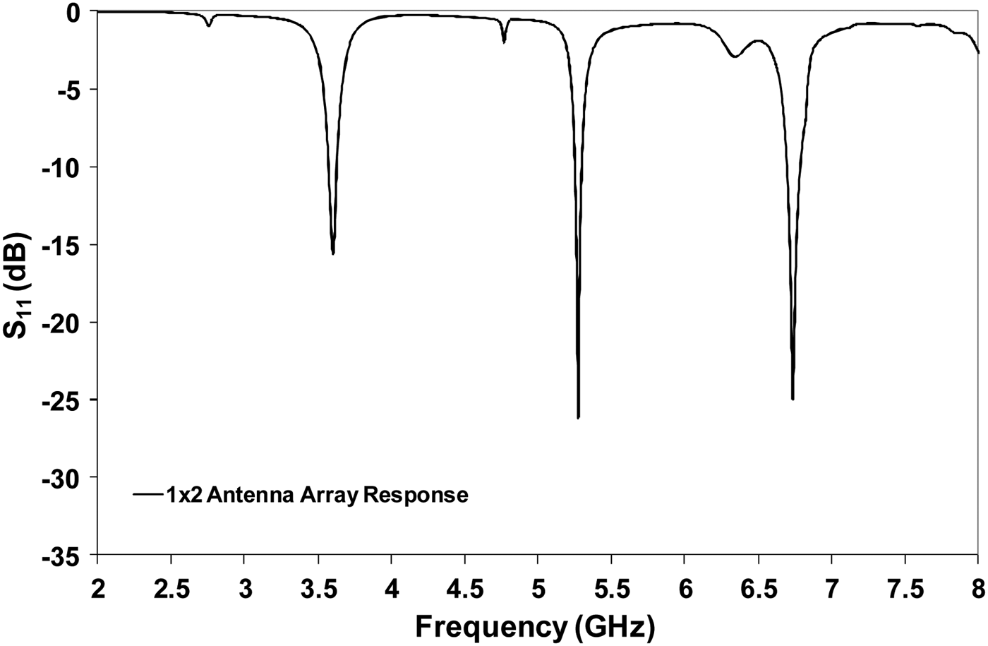
The width of the transmission lines was calculated using the ADS LineCalc tool. The calculated widths of the transmission lines are 3.5, 0.83, and 1.9 mm for 50, 100, and 70.7 Ω, respectively. The S 11 plot of the 1 × 2 triple-band antenna array is shown in Fig. 10 below. It can be seen from Fig. 10 that the simulated values of S 11 at 3.6 GHz is −15.6 dB, 5.2 GHz is −26.1 dB, and 6.7 GHz is −24.9 dB, respectively. The 10 dB impedance bandwidth of the array at 3.6, 5.2, and 6.7 GHz is 60, 55, and 110 MHz, respectively.
Fig. 10. S 11 plot of the 1 × 2 triple-band antenna array.
B) 1× 4 triple-band antenna array design
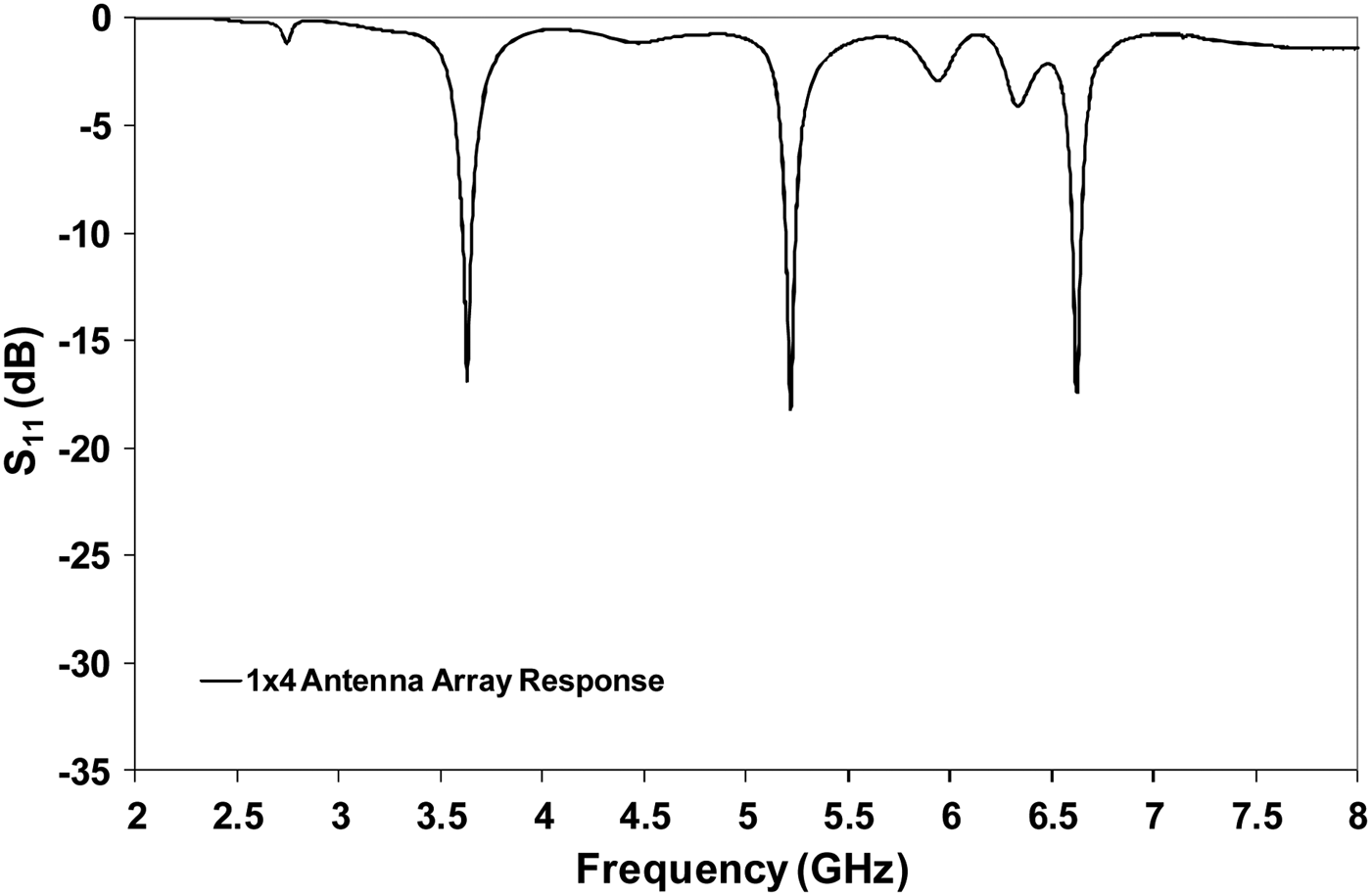
The proposed triple-band 1 × 4 antenna array design is presented in Fig. 11. The array is designed using two 1 × 2 array configurations joined together using a proper feed network, so all the impedances are matched to 50 Ω from the feed-point to the patch elements. The proposed 1 × 4 array gives better performance in terms of gain, directivity, and efficiency, as expected. Similar patch and feeding network dimensions are used in the design as depicted in Fig. 11. The S 11 plots of the 1 × 4 triple-band antenna array is shown in Fig. 12. It can be seen from the simulation results that the S 11 is −16.9 dB at 3.6 GHz, −18.2 dB at 5.2 GHz, and −17.4 dB at 6.7 GHz.
Fig. 11. Schematic representation of a triple-band 1 × 4 antenna array.
Fig. 12. S 11 plot of the 1 × 4 triple-band antenna array.
The 10 dB impedance bandwidth of the 1 × 4 array is 60, 75, and 70 MHz at 3.6, 5.2, and 6.7 GHz, respectively. It can be seen here that the antenna bandwidth is reduced as compare to 1 × 2 array for 6.7 GHz band which suggests that these are not the optimized results and the performance in term of S 11 and the bandwidth can be further improved by optimizing the lengths of all the transmission lines.
C) Antenna array gain, directivity, and efficiency
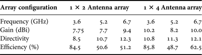
A performance comparison in terms of antenna array gain, directivity, and efficiency for both 1 × 2 and 1 × 4 configurations is studied in this section. Figures 13(a)–13(f) show the gain and directivity for triple-band 1 × 2 and 1 × 4 antenna arrays, respectively, and the same is summarized in Table 3.
Fig. 13. Simulated gain and directivity of triple-band 1 × 2 (a–c) and 1 × 4 (d–f) antenna arrays at 3.6 GHz (a, d), 5.2 GHz (b, e), and 6.7 GHz (c, f), respectively.
Table 3. Comparison of triple-band antenna array gain, directivity, and efficiency.
It can be observed from Figs 13(a)–13(c) that the simulated gain of the 1 × 2 antenna array is 7.75 dBi at 3.6 GHz, 7.7 dBi at 5.2 GHz, and 9.4 dBi at 6.7 GHz, respectively. The given patterns are the horizontal cut of the 3D radiation pattern at φ = 0° and θ = 0°–360° with infinite ground plane taken in the simulations, resulting in no back lobes. It is important to note from Figs 13(d)–13(f) that there is an increase in antenna array gains for 1 × 4 configuration for all three resonant frequencies. This is due to the fact that two more antenna elements are introduced in 1 × 4 array configuration. The achieved gain for 1 × 4 antenna array is 10.2 dBi at 3.6 GHz, 8.2 dBi at 5.2 GHz, and 10 dBi at 6.7 GHz, respectively. Furthermore, the comparison of results in Table 3 suggests that there is an improvement in antenna directivity for the first two resonant frequencies when the antenna elements are increased in the array. The smart antenna beam-steering [Reference Chang, York, Hall and Itoh23] operation can also be achieved using both the antenna arrays by wisely changing the signal phase, a number of techniques have been reported in the past to implement this [Reference Chang, York, Hall and Itoh23]. It can be observed from Table 3 that the efficiency is approximately similar for both 1 × 2 and 1 × 4 array configurations for the first two resonant frequency bands. Although it is significantly improved from 51.2% (1 × 2 array) to 62.5% (1 × 4 array) for 6.7 GHz band, it is important to mention that in multi-band antennas, slightly lower performance in terms of efficiency is typically observed at secondary frequency bands as compare to the primary frequency band.
This is a well-known phenomenon reported previously for multi-band antennas [Reference Maci and Gentili2, Reference Costantine, Kabalan, EI-Hajj and Rammal10]. Figures 14(a)–14(f) show the 3D radiation patterns of the 1 × 2 and 1 × 4 antenna arrays, respectively. For better realization, the pattern orientation shown is for φ = 0°–180° and θ = −90° to +90°. It can be seen from Figs 14(a)–14(f) that the stable radiation patterns are observed for all the resonant frequencies which suggests good antenna performance over these operating bands. Another important behavior which can be observed from Fig. 14 that the trend of change in radiation patterns for both antenna array configurations are similar as the resonant frequencies are increased from 3.6 to 6.7 GHz.
Fig. 14. Simulated 3D radiation pattern of the triple-band 1 × 2 (a–c) and 1 × 4 (d–f) antenna arrays at 3.6 GHz (a, d), 5.2 GHz (b, e), and 6.7 GHz (c, f), respectively.
V. CONCLUSION
This paper has presented the design of triple-band 1 × 2 and 1 × 4 slit-based printed antenna arrays for next-generation wireless and satellite-based applications. The antenna works on 3.6, 5.2, and 6.7 GHz frequency bands. From the proposed design, it can be seen that the antenna is simple and easy to fabricate using two symmetrical slits that made the antenna to resonate at three different frequency bands. For the proof-of-concept, the single-element triple-band antenna is fabricated and characterized, and a comparison between the simulated and measured antenna is presented. Different antenna performance parameters such as S 11, gain, directivity, radiation pattern, and bandwidth have been studied and analyzed.
The simulated results show that the designed antenna arrays have the impedance bandwidth of 1.67% at 3.6 GHz, 1.06% at 5.2 GHz, and 1.65% at 6.7 GHz for 1 × 2 configuration and 1.67% at 3.6 GHz, 1.45% at 5.2 GHz, and 1.05% at 6.7 GHz for 1 × 4 configuration, respectively. The proposed antenna arrays can be used for the next-generation software defined radios and radar-based application [Reference Christodoulou, Tawk, Lane and Erwin4], which requires reconfigurable antennas that can operate on multiple frequency bands. Moreover, the 5-GHz band operation allows these antenna arrays to be used in the next-generation WLANs IEEE 802.11 (ac) applications, which require smart-antennas with beam-steering capabilities [Reference Roh24]. Investigation on further suppression of back lobes by array optimization and fabrication of triple-band 1 × 2 and 1 × 4 antenna arrays will be performed using the FR4 substrate to compare the performance of the arrays with the simulation results which is subject to the future work.
Asghar Razzaqi received the Engineering degree in Electronics Engineering from National University of Sciences and Technology (NUST). He is presently doing his M.S. in Communication Engineering from NUST. His main research interests are in designing and optimization of RF and microwave devices particularly Antenna designing.
Dr. Bilal A. Khawaja received the B.S. degree in Computer Engineering from Sir Syed University of Engineering and Technology, Karachi, Pakistan, in 2002; the M.Sc. degree in Communication Engineering and Signal Processing from the University of Plymouth, Plymouth, UK, in 2005; and the Ph.D. degree in Electrical Engineering from the University of Bristol, Bristol, UK in 2010. Since August 2010, he has been working as an Assistant Professor in the Electronics and Power Engineering Department, at National University of Sciences and Technology (NUST), Karachi, Pakistan. His research interests are in antenna array designing for next-generation wireless systems and body area networks. He is also actively involved in the research related to microwave and millimeter-wave frequency band next-generation radio-over-fiber (RoF) systems, optical communication systems, and mode-locked lasers. He has also been a member of IEEE, USA since 2007.
Mehrab Ramzan received his BS in Telecommunication Engineering from NUCES, Pakistan in 2011. He is currently pursuing his MS degree in Electrical Engineering at Bilkent University, Turkey. His research interests are in smart TeraHertz and RF antennas and surfaces and use of microfabrication techniques to produce such antennas.
Muhammad Javed Zafar received Engineering degree in Electronics from National University of Sciences and Technology (NUST), Pakistan. He is presently doing his MS in Communication Engineering from NUST, Pakistan. His research interest are in designing and optimization of RF and microwave devices particularly wearable ultra wide-band (UWB) antennas.
Syeda Areeba Nasir received Engineering degree in Electronics Engineering from Sir Syed University of Engineering and Technology (SSUET), Pakistan. At present, she is doing her MS in Electrical Engineering with majors in Communication from National University of Sciences and Technology (NUST), Pakistan. Her main research interests are in radio electronics and RF planning and optimization.
Muhammed Mustaqim received the BS from USA, in 2007 and MS from Pakistan in 2012 and currently pursuing his PhD. His research interests are in wireless networks, RF and microwave systems.
Dr. Munir A. Tarar completed his B.Sc. in Electrical Engineering from the UET, Taxila, Pakistan, in 1995; Master of Space Studies from International Space University, France, in 1999; and Ph.D. in Electrical Engineering from Dalhousie University, Canada, in February 2010. Since March 2010, he has been working as an Assistant Professor at the Department of Electrical Engineering, School of Electrical Engineering and Computer Science (SEECS), National University of Sciences and Technology (NUST), Islamabad, Pakistan. He, currently, is appointed as the HoD, Research Institute for Microwave & Millimeterwave Studies (RIMMS). He has more than 14 years of practical experience in RF & Microwave engineering design and development, both at the circuits and systems level. He has been working also as R&D Consultant for the related industry. He has worked at the individual level as well as in team setups including responsibilities such as Design Engineer and Lead of a group of engineering professionals. He has been a Member, IEEE, USA, since 2004 and Professional Engineer, PEC, Pakistan, since 1995. He has been a volunteer IEEE Reviewer since 2007, organizer IEEE ICET 2011, and member TPC IBCAST and FIT Conferences.
Dr. Tauseef Tauqeer obtained the B.E. degree in Electronics Engineering from the Ghulam Ishaq Khan Institute of Engineering Sciences and Technology (GIKI), Swabi, Pakistan in 2005. He received the M.Sc. degree in Communication Engineering and the Ph.D. degree in Microelectronics and Nanostructures, both from the University of Manchester, Manchester, UK, in 2006 and 2009, respectively. During his studies, he was involved in the design and fabrication of InP-based low-power gigahertz-class Analog-to-Digital converters for the International Square Kilometre Array (SKA) radio telescope. He is currently working as an Assistant Professor and Head of the Department of Electronics, Power, and Control in the School of Electrical Engineering and Computer Sciences (SEECS), National University of Sciences and Technology (NUST), Islamabad, Pakistan. His research interests are in the field of MMICs, Antennas, HBTs, ADCs, and the physical & parametrical modeling of III–V-based semiconductor devices.