I. INTRODUCTION
The square kilometer array (SKA) [Reference Dewdney, Hall, Schilizzi and Lazio1] will be a next generation, ground based, radio telescope that will provide unsurpassed sensitivity and multiple beams of high resolution in the radio frequency window from 70 MHz to 30 GHz and will be operational below 10 GHz by 2022. It will be built to further the understanding of phenomena in the Universe. To help define the requirements, consideration has been focused on five Key Science Projects (KSPs) [Reference Carilli and Rawlings2].
The technical specifications [Reference Schilizzi3] are derived from the KSP, but are constrained by other aspects of design, such as feasibility and cost. The construction will be determined by the results of ongoing pathfinder projects and design studies [Reference Greenwood4]. Two such projects require a large number of amplifiers for their aperture array tiles [Reference Kant, Patel, Wijnholds, Ruiter and van der Wal5] and phased array feeds [Reference van Cappellen and Bakker6]. As the size of these feeds precludes cryogenic cooling, room temperature amplifiers are used.
The excellent input matching over broad bandwidth makes balanced amplifiers a serious candidate for the first stage low-noise amplifier (LNA) of these systems, despite the increased noise temperature with respect to single-ended amplifiers. Nevertheless, lowest possible noise performance is of utmost importance for the SKA and minimizing noise contributions to the system noise budget is essential to obtain this goal of 40 and 55 K (noise figure (NF) of 0.56 and 0.75 dB) [Reference bij de Vaate, Bakker, Woestenburg, Witvers, Kant and van Cappellen7], respectively.
One such noise contribution is the noise coupling between the antenna elements of the array systems being considered for the SKA, which may result in increased system noise temperatures due to a changing active reflection coefficient at the antenna ports as a function of beam steering [Reference Warnick, Woestenburg, Belostotski and Russer8, Reference Woestenburg, Bakker and Ivashina9]. This change in the active reflection coefficient is a result of the coupling between antenna elements and the way the output signals are combined during signal processing to alter the beam pattern of the array. The sensitivity of the noise temperature of the amplifiers to impedance changes at their inputs, defined by its noise resistance, R n, should be as small as possible.
In this paper, following on the previous work [Reference Woestenburg10], the noise parameters of the balanced amplifier are studied in order to find a way to reduce R n without a significant negative effect on the amplifier's noise, match and gain properties.
II. THEORY
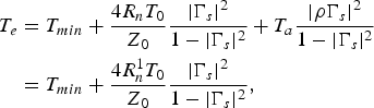
The noise temperature, T e, of an LNA as a function of its set of noise parameters is given by [Reference Woestenburg10]
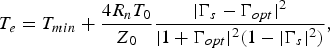 $$T_e=T_{min}+{4R_n T_0\over Z_0} {\vert \Gamma_s-\Gamma_{opt} \vert^2\over \vert 1+\Gamma_{opt} \vert^2\lpar 1-\vert \Gamma_s \vert^2\rpar } \comma$$
where T min is the minimum noise temperature, R n is the noise resistance, T 0 is the IEEE defined standard temperature of 290 K, Z 0 is the characteristic impedance at the output of the antenna element, Γs is the source reflection coefficient and Γopt is the optimal source reflection coefficient that results in minimum noise temperature.
The ultimate goal in LNA design is to achieve the minimal noise temperature, T min, by providing the optimum source reflection coefficient, Γopt, at the LNA input by transformation of the source impedance to the optimum impedance with a matching circuit, as depicted in Fig. 1. However, this does not provide simultaneous power and noise matching at the LNA input, but achieves noise match at the expense of a high-input reflection coefficient ρ.

Fig. 1. Diagram of noise-matched amplifier, with the source impedance transformed to the optimal source impedance to achieve minimal noise temperature at the expense of high input reflection.
The balanced amplifier provides a solution for simultaneous noise and power matching, at octave bandwidths required by the SKA. Power matching at the input of the balanced amplifier is achieved by placing two noise-matched LNAs in a configuration with quadrature couplers, as depicted in Fig. 2. The high-input reflections of the LNA are cancelled at the load termination on the input quadrature coupler, denoted as Z 0, while maintaining the LNA gain and noise properties.

Fig. 2. Diagram of power-matched balanced amplifier, where the high-input reflection of the noise-matched amplifiers is cancelled at the load termination on the input quadrature coupler.
The component amplifiers are ideally noise matched to Z 0. This follows from the definition of the component amplifiers in [Reference Woestenburg10]. If the condition of ideal noise matching to Z 0 is not fulfilled, then the resulting component amplifiers effective noise temperature will increase with respect to T min, but the effect of the termination on the fourth port of the quadrature coupler on the noise temperature sensitivity for impedance variations at the balanced amplifier input remains the same.
Apart from the noise resistance, the noise parameters of an ideal balanced amplifier are equal to those of the two component amplifiers, for the case when the two component amplifiers are both ideally noise matched to Z 0 and that the quadrature couplers are ideal over the whole band. This is because part of the noise generated in the load termination on the input quadrature coupler, Z 0 at ambient temperature T a, will be reflected at the input port of the balanced amplifier when the input port is not power matched. This will have a considerable contribution when the source input port is not ideally power matched [Reference Kerr11].
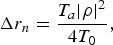
The noise temperature, T e, of a balanced amplifier as a function of its noise parameters is derived by referring the noise from the component amplifiers, as given by (1), to the input port of the balanced amplifier and by taking into account the noise from the input termination, resulting in [Reference Woestenburg10]
 $$\eqalign{T_{e} &= T_{min}+{4R_{n}T_0 \over {Z_0 }} {\vert \Gamma _{s} \vert ^2 \over 1 -\vert \Gamma _{s} \vert ^2} + T_{a} {\vert \rho \Gamma _{s} \vert ^2 \over 1 - \vert \Gamma _{s} \vert ^2 } \cr &= T_{min}+{4R_{n}^{1} T_{0} \over {Z_0 }} {\vert \Gamma _{s} \vert ^2 \over 1 - \vert \Gamma _{s} \vert ^2}\comma \; }$$
where R n is the noise resistance of the noise-matched component amplifiers (Γopt = 0), R n1 is the noise resistance of the balanced amplifier and T a is the ambient temperature.
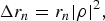
Using (2), the increase in the normalized noise resistance of the balanced amplifier, R n1/Z 0, with respect to the normalized noise resistance of the component amplifier, R n/Z 0, is
 $$\Delta r_{n}={T_a \vert \rho \vert^2 \over 4T_0} \comma \;$$
where the increase in r n for poorly power-matched component amplifiers of a room temperature balanced amplifier has a maximum value of 0.25. For component amplifiers with moderate input reflection coefficient, Δr n will be reduced proportionally to |ρ|2.
Replacing the termination on the input coupler by a short circuit would effectively eliminate its noise contribution. However, instead of being absorbed by the termination, the reflected signals emerging from the inputs of the component amplifiers will now be reflected at the short-circuit termination and will enhance the noise power emerging from the balanced amplifier input with a factor of 1+|ρ|2, making the noise behavior more sensitive to input reflections.
The increase in normalized noise resistance of the balanced amplifier, R n1/Z 0, with respect to the normalized noise resistance of the component amplifier, R n/Z 0, becomes
 $$\Delta {r_ {n}} = r_{n} \vert \rho \vert ^2\comma \;$$
where the maximum increased r n value of the balanced amplifier would be twice that of the component amplifiers. In general, the increased r n value with a short circuit will be lower than with a matched termination at the input coupler port. However, having a short-circuit termination will cause considerable deterioration of the balanced amplifier's input match.
Although it would result in an input reflection coefficient ρ2 compared to zero-input reflection coefficient for a balanced amplifier with a load termination on the input coupler, having a short-circuit termination gives an improvement in return loss of a factor of two, with respect to that of the component amplifiers. In some cases, the trade off between input matching and noise performance, low r n and low sensitivity to varying source impedance, could result in a choice for this solution.
III. DESIGN FOR OPTIMUM SENSITIVITY AND MATCHING
Two expressions for the increase in r n have been given with respect to the component amplifiers, for a balanced amplifier with ideal and deteriorated input matching determined by the input coupler load. In practice a compromise may be found witha a load resistor value between 50 and 0 Ω, leading to acceptable input matching and sensitivity to source impedance variations, by optimizing an LNA design with the load resistor value as a free parameter.
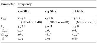
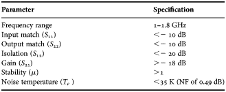
In order to test whether this method leads to a potential solution for the SKA, a balanced amplifier was designed to meet the first stage LNA specifications of Aperture Tile in Focus (APERTIF) [Reference van Cappellen and Bakker6], as defined in Table 1. The emphasisis on maintaining the match, gain and noise properties of the standard balanced amplifier, but with a decreased sensitivity to source impedance changes, for example due to changes in the active reflection coefficient at the input port as a function of beam steering.
Table 1. LNA specifications.
To simplify the design, an application board for a balanced amplifier making use of dual low-noise integrated amplifiers operating over this frequency range is used [12]. The amplifiers' noise parameters, as well as their input reflection coefficients, at three frequencies are given in Table 2. The noise parameters are very appealing; however, the high-input reflection coefficient needs to be reduced in this configuration.
Table 2. Component amplifier noise parameters and input reflection.

The lumped element values of the matching components of the original balanced amplifier design are recalculated to find a compromise between: (1) the nearly ideal input power match obtained when using a input load termination of Z 0 with relatively large r n value; and (2) the reduced sensitivity to a varying source impedance, with the value of the load termination of the input coupler kept to a minimum.
The combination of the low values for the noise parameters of the component amplifiers and the decreased sensitivity to a varying source impedance, would make this balanced amplifier configuration ideal for beam steering.
IV. RESULTS
The amplifier was designed in AWR MWO, using the circuit model of the application board, as depicted in Fig. 3. The core component of the balanced amplifier is the dual low-noise integrated amplifier in the middle of the circuit, X 3. This component's noise properties are optimized around 1.4 GHz by selecting appropriate values for the four transmission lines, T 1, …, 4, the four inductors, L 1, …, 4, and six of the capacitors, C 1, …, 6,. Also, this component's bias settings are optimized for noise performance around 1.4 GHz by selecting appropriate values for four of the resistors, R 1, …, 4,. Bias stability is maintained by selecting appropriate values for the other eight capacitors, C 7, …, 14,. The balanced amplifier is power matched by placing this circuitry within the two quadrature couplers, X 1,2, with load terminations Z 0 and R 6.

Fig. 3. Circuit Diagram of Application Board, with the termination on the input coupler replaced by a variable impedance to improve the sensitivity to a varying source impedance.
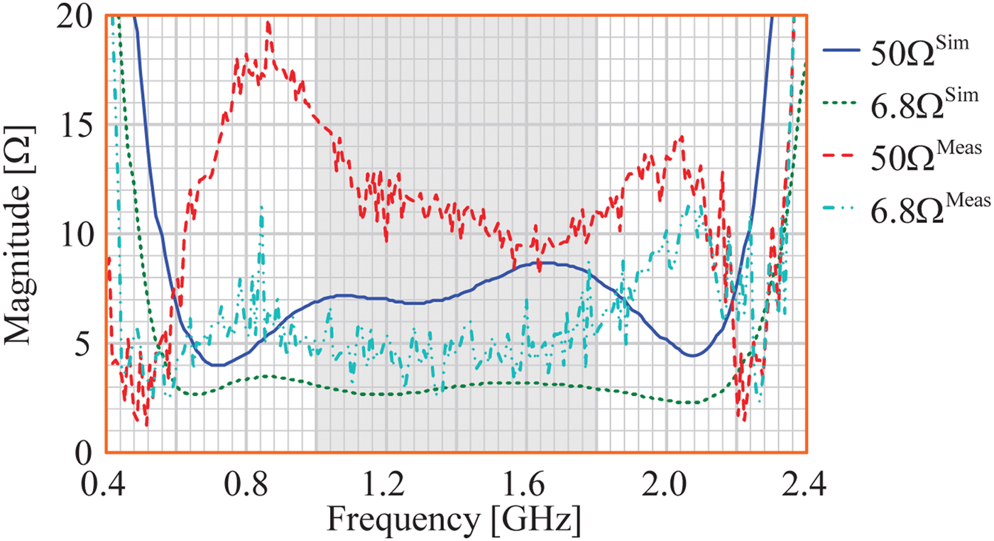
The design process began with the ideal components specified for the load termination circuit. Firstly, the termination on the input coupler, Z 0, was replaced by a short circuit to compare with the theory of Section II. The simulated results of the balanced amplifier with 50 and 0 Ω termination loads on the input coupler are compared with that of the single-ended amplifier device in Figs. 4 and 5. As expected, Fig. 4 shows that the noise resistance of the balanced amplifier is greater than the noise resistance of the component amplifiers, on average from 3.0 to 7.6 Ω. In replacing the load termination on the input coupler of 50 Ω with a short circuit, this is greatly reduced, on average to 1.9 Ω. Coupled to this is a slight reduction in the noise temperature, on average from 27 to 25 K (NF of 0.39–0.36 dB).

Fig. 4. Simulated noise resistance results, where the noise resistance of the balanced amplifier is greatly reduced by terminating the input coupler with a short.

Fig. 5. Simulated input matching results, where the power match of the balanced amplifier is considerably deteriorated by terminating the input coupler with a short.
However, as expected, there is considerable deterioration in the input match, on average from S 11 < −6 dB to S 11 <− 4 dB, as depicted in Fig. 5, due to the short-circuit termination. Another disadvantage is that the balanced amplifier is no longer unconditionally stable. As a result, the short-circuit option cannot be properly characterized on the measurement equipment, so no measurement results for the short-circuit option are presented here. As a solution, a compromise must be found with a load resistor value between 50 and 0 Ω that leads to acceptable input matching and sensitivity to source impedance variations, as well as proper stability.
As the load termination is no longer equal to the characteristic impedance, it no longer fully absorbs the poor input match of a component amplifier optimally matched to noise. Therefore, the lumped elements are now required to perform both noise and power matching, as depicted in Fig. 6, with arrows used to indicate the lumped elements that were optimized. At the same time, the value of the load termination is kept as low as possible to improve the sensitivity to a varying source impedance. The result is a 6.8 Ω load termination on the input coupler.

Fig. 6. Circuit diagram of application board, with arrows used to indicate the lumped elements that are optimized to achieve both noise and power matching.
The parameters of the original design with 50 Ω load, as well as with 6.8 Ω load, are measured on the Agilent N5242A PNA-X Network Analyser in a Faraday cage to shield from radio frequency interference (RFI). The measured results of the balanced amplifier with 50 and 6.8 Ω termination loads on the input coupler are compared with their simulations in Figs. 7–10.

Fig. 7. Simulated and measured input matching results, where a reasonable power match has been achieved by optimizing the lumped elements to achieve both noise and power matching.

Fig. 8. Simulated and measured stability results, where the unconditional stability of the balanced amplifier has been restored by optimizing the lumped elements.

Fig. 9. Simulated and measured noise resistance results, where the noise resistance of the balanced amplifier is more than halved by terminating the input coupler with a 6.8 Ω load.

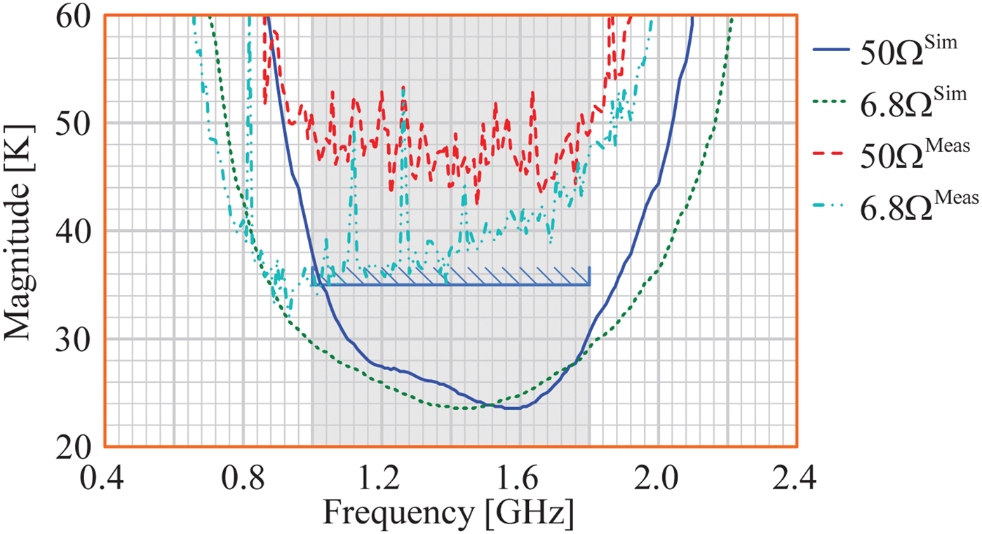
Fig. 10. Simulated and measured noise temperature results, where the noise temperature of the balanced amplifier is slightly reduced by terminating the input coupler with a 6.8 Ω load.
The configurations are well input matched, S 11 < −10 dB, as depicted in Fig. 7. As expected, the 50 Ω configuration achieves a better match due to the absorption of the reflected signals at the load terminations. The simulations predict the measurements with reasonable accuracy, with differences due to the simplified circuit model used in the design process.
The two designs are well output matched, S 22 < −18 dB, have good isolation, S 12 < −24 dB, and have decent gain for one stage amplifiers, S 21 > 18 dB. The 50 Ω design achieves slightly better output match and gain, but slightly lower isolation. While the simulations do not predict the measurements with absolute accuracy due to the simplified circuit model used in the design process, the shapes of the simulations and measurements are similar.
Both designs are unconditionally stable, μ > 1.2, as depicted in Fig. 8. This parameter is important in beam steering, as the varying source impedance could cause the balanced amplifier to oscillate if it were not unconditionally stable.Once again, the disparity between results is due to the simplified circuit model used in the design.
Fig. 9 shows that the noise resistance of the amplifier is more than halved, on average from 11 to 4.8 Ω, due to the reduction of the load termination on the input coupler from 50 to 6.8 Ω. Coupled to this is a reduction in the noise temperature, on average from 48 to 40 K (NF of 0.67 dB to 0.56 dB), as depicted in Fig. 10. The reasons for the difference between the simulations and noise measurements is still being investigated.
As an example, the increase in the noise temperature is calculated from the results for a change in the antenna impedance from 50 to 43.3 + j25 Ω due to beam steering. The sensitivity is more than halved in using the 6.8 Ω load instead of the 50 Ω load, on average resulting in a reduction of the noise temperature increase from 25 to 10 K (NF of 0.36–0.15 dB), as depicted in Fig. 11.

Fig. 11. Simulated effect of noise temperature sensitivity, where the sensitivity to changes in the source impedance is more than halved by terminating the input coupler with a 6.8 Ω load.
V. CONCLUSION
Traditionally, balanced amplifiers have superior power-matching properties over wide bandwidth compared to single-ended amplifiers. However, at a cost of an increased noise temperature due to the losses in the couplers. Recently, balanced amplifiers with very low-noise properties have become available [12]. However, if such an amplifier was used in a beam-steering system, the noise generated in the load termination of the input coupler would deteriorate the amplifier noise resistance, thereby increasing the noise temperature due to a varying active reflection coefficient at the antenna ports as a function of scan angle.
Replacement of the input coupler's load termination of the basic balanced amplifier by a short circuit reduces the sensitivity of the noise temperature to source impedance variations, but deteriorates the input reflection coefficient. However, if the lumped elements of the matching networks are reoptimized for both noise and power properties, a balanced amplifier can be built that compromises some of its nearly ideal input power match for a reduced sensitivity to a varying source impedance, thereby making this configuration favorable for applications in radio astronomy-phased array systems.
ACKNOWLEDGEMENTS
The first author acknowledges NRF for funding this work and ASTRON for hosting him at their institute.
 David Smith received his BEng, MScEng and PhD in Electronic Engineering from Stellenbosch University in 2001–2010. From 2010 to 2011, he held a post doctoral position at Stellenbosch University working on an LNA for APERTIF, an SKA Pathfinder Project. Currently, he holds a post doctoral position at ASTRON working on the OLFAR Project.
 Bert Woestenburg received his degree in Microwave Engineering from Twente University in 1983. He has been involved in the design of LNAs and receiver systems, mainly for the WSRT, since the start of his professional career at ASTRON. Currently, he is the head of the RF & Low Noise Systems group at ASTRON. His interests lie in the design of LNAs and the noise characterization of aperture arrays and PAF systems.