


Introduction
Metasurfaces (MSs) are two-dimensional equivalents of volume metamaterials. They have attracted researchers to work on them due to their attractive features such as concise planar structure, low losses, and low cost. [Reference Holloway, Dienstfrey, Kuester, O'Hara, Azad and Taylor1–Reference Yu and Capasso3] MS are able to influence electromagnetic waves, and thus find a very wide area of applications such as miniaturization of cavity resonators [Reference Caiazzo, Maci and Engheta4], controllable and smart surfaces [Reference Hollowary, Mohamed, Kuester and Dienstfrey5], and improvement in the performance of patch antennas [Reference Chung and Chaimool6, Reference Islam, Ullah, Singh and Faruque7]. MS-based structures, which comprise high impedance structure [Reference Sievenpiper, Zhang, Broas, Alexopolous and Yablonovitch8], reactive impedance surfaces [Reference Bernard, Chertier and Sauleau9, Reference Agarwal, Nasimuddin and Alphones10], and electromagnetic bandgap structures (EBG) [Reference Yang and Rahmat-Samii11], have been implemented on antennas to improve their performance. EBG MSs are periodic structures with subwavelength dimensions, intended to form an artificial magnetic conductor. These structures show a high-impedance behavior, and electromagnetic waves are reflected from them with zero degree reflection phase, thus showing in-phase reflection properties too. A lot of work has been performed by various researchers on MS-based antennas for enhancing their performance. In [Reference Chaimool, Rakluea and Akkaraekthalin12], a MS superstrate comprising square loop resonators was loaded on a slot antenna to improve the gain, bandwidth, and radiation at 2.45 GHz. By using a left-hand material-based MS, the RCS reduction was obtained [Reference Wang, Hong and Gong13]. The use of MS linear-to-circular polarization conversion was also presented in [Reference Zhu, Chung, Sun, Cheung and Yuk14, Reference Da Silva, Da Silva, De Siqueira Campos and De Andrade15]. However, the above works showed limitation of the antenna, which is compact due to the presence of an air gap between the MS and the antenna.
Nowadays, the importance of circularly polarized (CP) antennas is increasing in wireless communication because of the independence of the alignment of the transmitter and the receiver which leads to the removal of polarization loss. Researchers have worked on the design of many CP antennas by using different methods which involved truncation, cutting of slots, slits on patch, and various other methods [Reference Huang, Yang, Li, Wang and Wen16–Reference Nasimuddin, Qing and Chen19]. Among the various methods, MSs proved to be efficient in generating CP waves and also in enhancing the performance of the antenna. The wide band and low-profile CP antennas have been designed, in which the patch antenna is placed either above or below the MS. In [Reference Zhu, Cheung and Chung20], a 2.45 GHz microstrip antenna was coupled to the MS and was able to convert the linearly polarized (LP) wave to CP waves with improved return loss and AR bandwidth. A CP slot antenna operating at 2.7 GHz was proposed [Reference Chung and Kharkovsky21] with a MS being placed above the patch and a metallic reflector at the bottom of the patch which achieved a 29% operating bandwidth along with a high front to back ratio. In [Reference Vijitsulakkana, Thaiwirot, Akkaraekthalin and Chaimool22], a MS with a slanted slot over a microstrip antenna placed at a height of 30 mm was able to generate CP wave as well as improved the gain of the antenna. In [Reference Nasimuddin, Chen and Qing23], a wide impedance bandwidth of 36% and an AR bandwidth of 8.3% was obtained by placing a rectangular ring MS array at a height of 1.6 mm from a ground plane and the rectangular slotted patch being placed above it at a height of 3.2 mm, also led to an increase in the size of the antenna as reported in [Reference Zhu, Cheung and Chung20–Reference Vijitsulakkana, Thaiwirot, Akkaraekthalin and Chaimool22]. A wideband MS-based CP antenna array was designed [Reference Zhu, Cheung, Liu and Yuk24] to obtain a high gain and impedance bandwidth by using a proper combination between the sequentially rotated feeding network and the CP MS-based antennas, thus leading to a complex method. In [Reference Xu, Wang, Liang, Qi and Gao25], a compact, single feed CP antenna was designed using a MS and meta-resonator and it was observed that the performance of the antenna improved. Using more than one MS, CP antennas were also designed to improve the performance of the antenna. In [Reference Burokur, Lepage, Varault, Begaud, Piau and de Lustrac26], by using two layers of MSs that are coupled to a microstrip patch antenna, two CP bands at 1.26 GHz and 1.56 GHz were obtained with improved gain. By using two compact MSs on a LP microstrip antenna [Reference Augusto, Montalvao, Neto, Campos and Silva27], it was possible to generate CP waves at 2.45 GHz and 5.8 GHz, having an impedance bandwidth of 340 MHz and 740 MHz, respectively; but it was observed that by placing the two MSs each at a distance of 9 mm from the antenna caused an overall increase in the size of the proposed antenna. A square-based MS CP antenna was designed at a Tetrahertz frequency, using a multiple-slit feeding structure [Reference Hussain and Parka28] and achieved a 3-dB gain bandwidth of 17.3%, but it led to fabrication complexity. Recently, a rectangular ring-shaped MS was placed below a slotted patch antenna [Reference Nasimuddin, Chen and Qing29] to achieve a wideband 3-dB AR bandwidth and showed that dimension of patch, the shape of the MS, and feed location led to improved performance. In [Reference Wu, Li, Li and Chen30] a slot coupling antenna and a polarization dependent MS array were placed in direct contact and thus achieved a wide AR bandwidth. In [Reference Zhipeng, Ouyang and Yang31], a CP MS antenna was proposed by implementing four silts and an L-type slot on the MS which leads to a wide impedance bandwidth of 18% and a 3 dB AR bandwidth of 12.8%.
With the view to achieve a compact size, a simple design, and easy fabrication with an improved performance of the CP antenna, a compact CP antenna with a low profile of 30 × 30 × 3.2 mm3 using MS-superstrate for the WiMAX (3.5 GHz) band is proposed in this article. Four EBG unit cells, comprising a slotted rectangular patch polarization-dependent MS superstrate, are organized in an array which is printed on a dielectric substrate for the wideband, and an inclined slot on the ground plane to achieve CP radiation is presented. This paper firstly discusses the proposed EBG-based MS structure and antenna geometry, followed by the parametric analysis to obtain optimized parameters. In the following sections, there is further discussion of the results of the proposed antenna.
Unit cell EBG-based MS
The two properties of the EBG-based MS that have been widely explored in the field of microwave antennas, leading to some improvements in the performance of the antenna [Reference Numan and Sharawi32], are: a MS forbids the propagation of the surface wave, and the in-phase reflection of incident waves makes them behave like an artificial magnetic conductor. The EBG frequency band-gap feature identification can be done by the transmission characteristics of a suspended microstrip line, dispersion diagram, and reflection phase characteristics, respectively [Reference Samineni and Khan33]. Figure 1 shows the detailed geometry of the single unit cell EBG, comprising a rectangular metal plate built on the FR4 substrate (ε r = 4.4 and tan ∂ = 0.01). The MS is formed with four rectangular metal patches arranged in a 2 × 2 layout with periodicity P = 12 mm, printed on the top side of the substrate of height h = 3.2 mm. Each unit cell of the MS superstrate has dimensions which are as follows: L = 11 mm, W = 10 mm,  $L_{u_1}$ = 7.5 mm,
  $L_{u_2}$ = 6.5 mm, Wu 1 = 8 mm,
  $W_{u_2}$ = 6.mm, and
  $W_{u_3}$ = 1 mm.

Fig. 1. Top view of the proposed EBG-based MS unit cell.
To know the operating frequency band of the proposed slotted MS, the scattering simulation is used and the reflection phase plotting of the EBG MS is performed, as shown in Fig. 2. By simulating a unit cell within the air box which is excited by a Floquet port, the four sides of the box are applied with periodic boundary conditions with a perfect matched layer placed on top of the unit cell [Reference Sievenpiper, Zhang, Broas, Alexopolous and Yablonovitch34]. In Fig. 3, the ± 90° reflection phase bandwidth [Reference Yang and Rahmat-Samii35] is 1.86–3.96 GHz, with the 0° reflection phase at a resonance frequency of 2.84 GHz. With the chosen optimized dimensions of the MS structure, it is observed that the frequency band gap (1.86–3.96 GHz) of the slotted MS unit cell coincides with the operating frequency band of the antenna, making the slotted MS unit cell suitable to be used for designing a wideband antenna.

Fig. 2. Simulation set up of EBG-based MS unit cell.

Fig. 3. Simulation results of the reflection phase for the EBG-based MS unit cell.
Proposed antenna structure and design
Figure 4 shows the geometry of the proposed CP antenna with a polarization-dependent slotted EBG-based MS superstrate. It comprises two parts: firstly, it is a 2 × 2 MS-superstrate array, consisting of four unit cells of rectangular patches with the U slot printed on a dielectric substrate, and secondly, an inclined slot introduced in the conventional coplanar (CPW) feed line on the ground plane. FR4 (dielectric constant = 4.4) with a height (h) of 3.2 mm is used as an antenna substrate as well as an MS substrate. For energy coupling between the CPW feed line and the MS-superstrate, an inclined slot with a length of 18 mm and a width of 3 mm is cut onto the ground plane. The overall dimension of the proposed antenna is 30 × 30 × 3.2 mm3. The conversion of the LP wave into CP is obtained by the slot on the ground which is inclined at an angle with the CPW feed line and the polarization dependent slot-loaded rectangular patches. The image of the fabricated model, the top and the bottom views are shown in Figs 5(a) and 5(b), respectively.
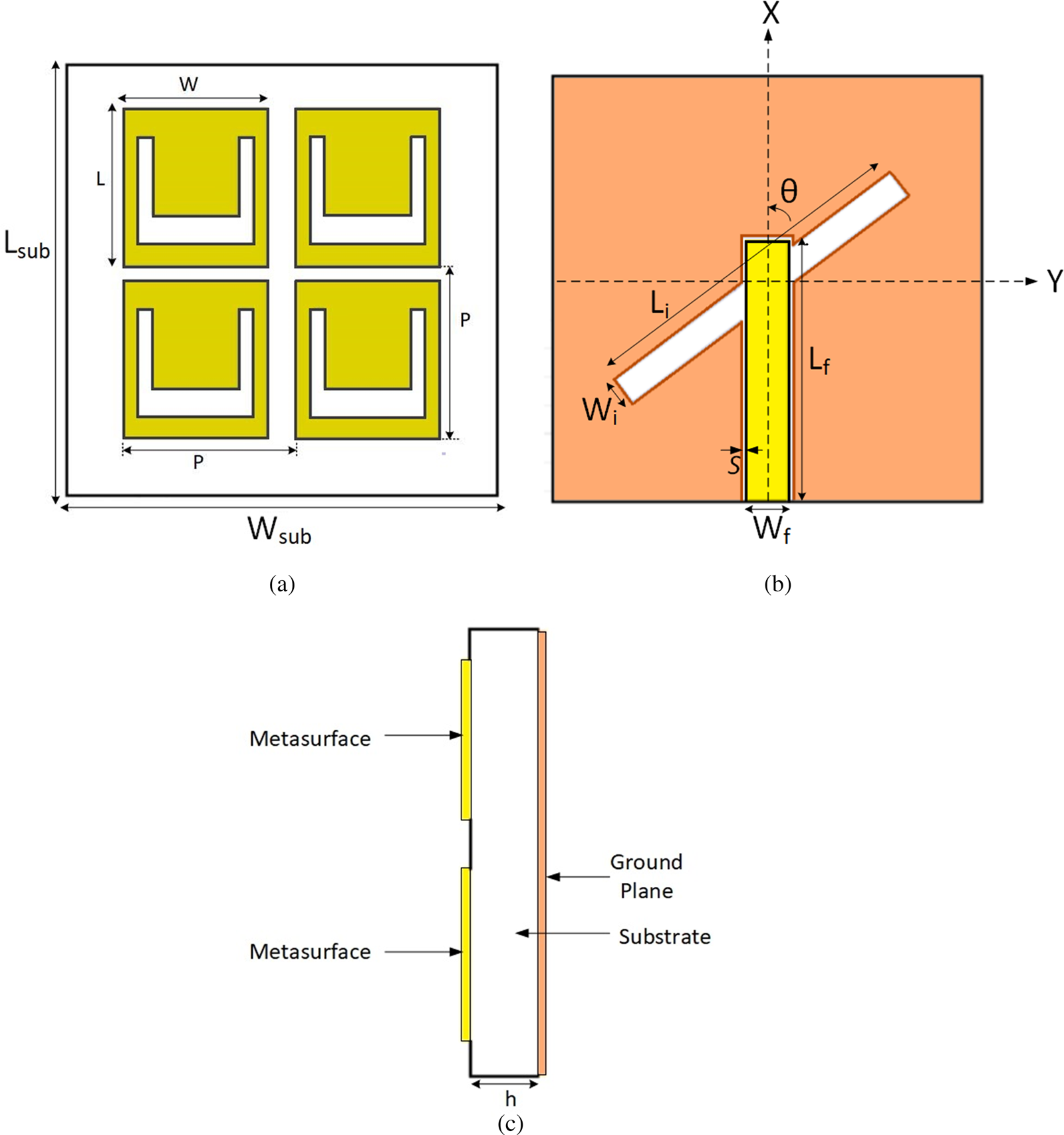
Fig. 4. (a) Top view of the proposed antenna: (b) bottom view and (c) side view.

Fig. 5. Fabricated model of the proposed antenna: (a) top view and (b) bottom view.
Parametric analysis of the proposed antenna
The proposed antenna was simulated by using the simulation software Ansoft HFSS v.15 and parametric analysis was performed to achieve circular polarization for the desired operating band. While performing the parametric analysis, one of the parameters was varied to study its effect on the antenna performance but the other parameters were fixed to a particular value. Table 1 shows the optimized value of the proposed CP antenna with a slotted MS. Using the optimized values, the antenna performance improved in terms of the impedance bandwidth, AR bandwidth, and gain.
Table 1. Parameters of the proposed antenna.

Using the optimized values of the proposed antenna, CP radiation was achieved with an improved performance in the operating band.
Variation of the inclined angle, θ
It is observed that the slot of the dimension of L i and W i is implemented in the CPW feed line with an inclination angle θ to the x-axis which affects the antenna performance. For different values of the inclined angle θ, the return loss characteristics are shown in Fig. 6. It is seen that as the inclination angle is increased from 52° to 54°, the impedance bandwidth increases. At θ = 54°, the impedance bandwidth is more, but no circular polarization is achieved. Finally, at θ = 53°, it is seen that the operating band is 815 MHz, which is wide, and thus, a good CP performance is achieved.

Fig. 6. Variation of return loss (simulated) with frequency for different values of the inclination angle (θ).
Variation of inner length of U slot in EBG MS superstrate,  $L_{u_2}$

The inner length of the U slot of the EBG MS superstrate,  $L_{u_2}$, was varied from 6.4 mm to 6.6 mm as shown in Fig. 7. For
  $L_{u_2}$ of 6.6 mm, the proposed antenna showed a good impedance matching and impedance bandwidth, but the circular polarization was not achieved. So, finally,
  $L_{u_2}$ was optimized to 6.5 mm as a wide impedance bandwidth and a good AR bandwidth was achieved.

Fig. 7. Variation of return loss (simulated) with frequency for different values of  $L_{u_2}$.
Variation of inner width of U slot in EBG MS superstrate, $W_{u_2}$

Figure 8 shows that the inner width of the U slot EBG MS superstrate was varied from 5 mm to 7 mm. It was observed that the impedance bandwidth decreases as the width increases. At  $W_{u_2}$ = 6 mm, the antenna showed good CP radiation over the desired operating band with an impedance bandwidth of 730 MHz. No CP radiation is observed at 5 mm and 7 mm, and so, the final value of
  $W_{u_2}$ is optimized to 6 mm.
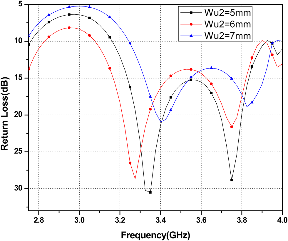
Fig. 8. Variation of return loss (simulated) with frequency for different values of  $W_{u_2}$.
Experimental results and discussion
With the help of an Agilent Vector Network Analyzer (N5230A: PNA-L), the measured results were taken and close agreement with the simulated results was obtained considering the fabrication tolerance and the measurement system error. Table 2 shows the comparison of our proposed antenna with some of the works given in the literature.
Table 2. Comparison table of reported MS-based CP antenna with our proposed antenna given in the literature.

Surface current distribution
The surface current distribution on the MS has been analyzed to find the influence of unit cell geometry on the mechanism of radiation at broadside. Figure 9 shows the simulated vector surface current distribution on the MS to vary with the phase at 3.20. This explains the polarization characteristic of our proposed antenna. It is observed that at instance θ = 0° and θ = 180°, the simulated vector currents are equal in magnitude but opposite in phase. Similarly, at θ = 90° and θ = 270°, the vector currents are equal and opposite in phase. Thus, it is observed that with a change in the phase, the surface current vector turns in the anticlockwise direction. Hence, it is concluded that the antenna radiates left-hand circular polarization (LHCP).

Fig. 9. Top view of the surface current density at (a) θ = 0°, (b) θ = 90°, (c) θ = 180°, and (d) θ = 270.
Return loss versus frequency
Figure 10 shows the measured and simulated return loss of the wideband CP antenna with the slotted MS superstrate. It is observed that without using MS, the antenna shows an impedance bandwidth of 280 MHz (3.62–3.34 GHz). On using the non-slotted MS the impedance bandwidth increases to 799 MHz (2.821–3.620 GHz). By implementing a slotted MS, two resonant modes are excited at 3.27 GHz and 3.75 GHz and thus a wide impedance bandwidth is achieved with simulated −10 dB return loss bandwidth of 815 MHz (3.077–3.892 GHz) at a center frequency of 3.48 GHz. The measured −10 dB return loss bandwidth is 1180 MHz (2.820–4.00 GHz), as required for a WiMAX band (3.5 GHz band).

Fig. 10. Variation of return loss bandwidth with frequency.
Axial ratio versus frequency
From Fig. 11, it is observed that without using the MS an AR bandwidth of 60 MHz (3.45–3.39 GHz) is achieved. It is also observed that a wideband simulated 3-dB AR bandwidth of 143 MHz (3.135−3.278 GHz) is obtained due to resonance modes created in this band, and that the slot loaded MS-superstrate achieves a better simulated AR bandwidth in comparison with an unslotted MS-superstrate which achieves an AR bandwidth of 100 MHz (3.31–3.41 GHz). The measured 3-dB AR bandwidth of the slot loaded MS-superstrate is 219 MHz (3.135–3.354 GHz) with a center frequency of 3.20 GHz which lies near to the first resonance of the impedance bandwidth and obtaining minimum AR of 0.68 dB.

Fig. 11. Variation of AR bandwidth with frequency.
Variation of gain with frequency
Figure 12 shows that without the MS the peak gain of the antenna is 2.66 dBi and the peak gain of the antenna without the slotted MS-superstrate is 3.47 dBi in the desired operating band. On using slotted MS superstrate, the simulated peak gain of the slot-loaded MS-superstrate antenna is 3.54 dBi for the desired operating band and the measured peak gain is 3.91 dBi which shows that there is a rise in the peak gain by 0.44 dBi as compared to the antenna without the slotted MS-superstrate. The CP waves radiated by the inclined slot are coupled between the feed line and MS and thus the radiated field expands over a larger radiating aperture, due to the implementation of MS which results in enhanced gain. Thus, we can conclude that the slotted MS-superstrate improves the performance of the proposed antenna.
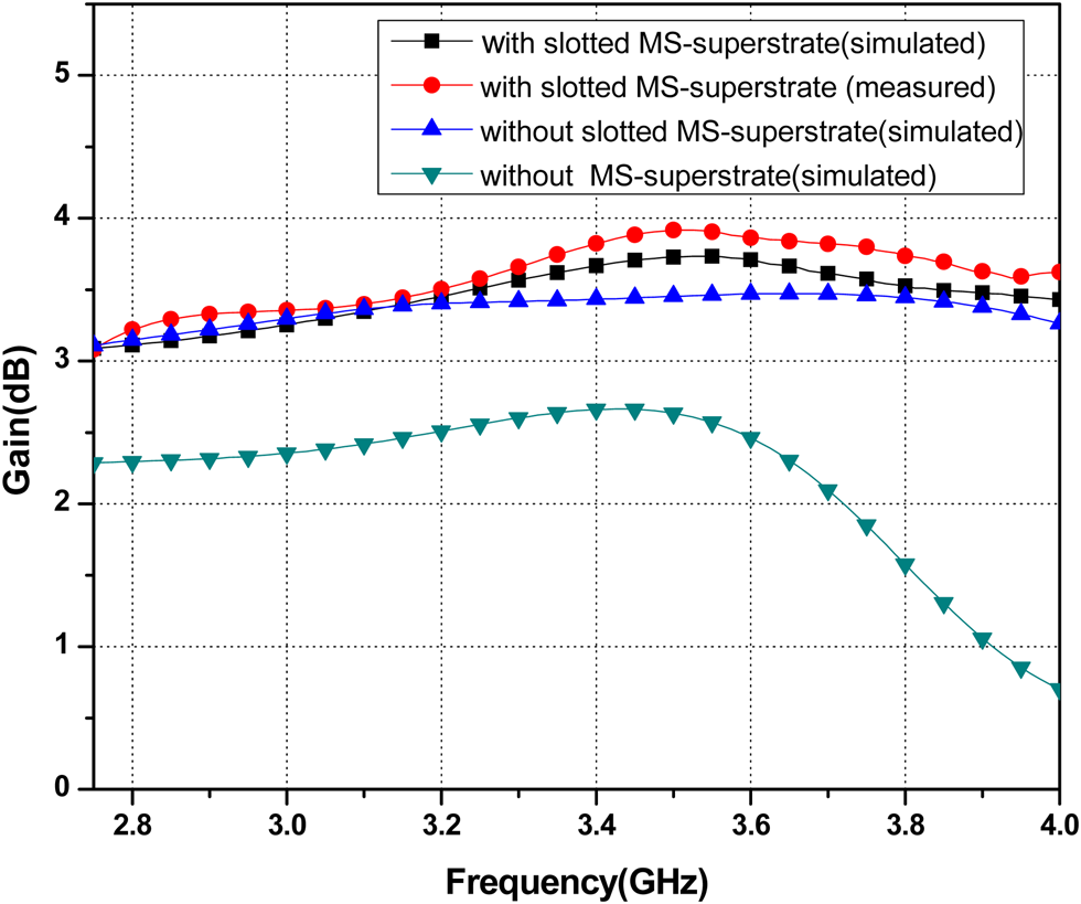
Fig. 12. Variation of gain with frequency.
Radiation pattern
The simulated and measured results of the radiation pattern are observed at 3.2 GHz and shown in Fig. 13. In the two planes x–z and y–z, it is observed that LHCP is obtained. It is also observed that the beam width extends to 55° (−28° to 27°) at the xz plane and 47° (−23.5° to 23.5°) at the yz plane. Figure 14 shows the 3D radiation pattern of the proposed antenna at 3.2 GHz. The analysis of the measured and the simulated results show some deviation, which may be due to the effect of fabrication imperfections and measurement errors.

Fig. 13. At 3.2 GHz the simulated and measured radiation pattern: (a) x–z plane and (b) y–z plane.

Fig. 14. 3D radiation pattern at 3.2 GHz.
Conclusion
A slotted EBG MS-based microstrip antenna is proposed in order to achieve wideband CP radiation at 3.2 GHz. Parametric analysis shows that performance enhancement of the proposed antenna is achieved by the slots on the MS, thus achieving 1180 MHz impedance bandwidth, with a 3-dB AR bandwidth of 219 MHz and a peak gain of 3.91 dBi at the operating bandwidth. The proposed antenna is compact, achieves wide impedance bandwidth and good AR bandwidth and is thus a promising structure for wireless communication, finding its application in a 3.5 GHz WiMAX band.
 Alka Verma received her B.E. degree in Electrical & Electronics from Bangalore University, Karnataka, India. She has completed M. Tech. Degree in Electronics Engineering from, Dr. A.P.J Abdul Kalam Technical University (formerly UPTU), Lucknow (U.P.), India and Pursuing Ph.D. degree from same. Her area of interests are microstrip antennas, electromagnetic band gap structures, and circularly polarized microstrip antenna for wireless communications.
 Dr. Anil Kumar Singh was born in Jamalpur, Mirzapur (UP), India in 1976. He has completed M. Tech. Degree in Instrumentation and Control Engineering from NITTTR Chandigarh, India and Ph.D. degree on Studies on Annular Ring Microstrip Antenna for different Applications from Electronics Engineering Department, Indian School of Mines (ISM), Dhanbad, (India). He joined the Department of Electronics and Instrumentation Engineering, Institute of Engineering and Technology, M. J. P. Rohilkhand University, Bareilly as a lecturer in 2002. He has published more than 20 papers in national and international journals and conferences. His current research interest includes design and analysis of microstrip antennas.
 Dr. Neelam Srivastava is working as a director in REC Kannauj (U.P.), India since 2016. She has completed her B.E. in Electronics Engineering from M.M.M. Engineering College, Gorakhpur, India in 1985. She did her M.Tech. from I.I.T. B.H.U., Varanasi, India in 1987 and Ph.D from Lucknow University, Lucknow, India in 2004. She has a keen research interest in optical communication, image processing, and microwave engineering.
 Dr. Shilpee Patil received her B.Tech. degree in Electronics & Communication Engineering from AKTU (formerly UPTU), Lucknow, India, and the M.Tech. degree in Digital Communication from GGSIP University, Delhi, India, in 2009. She pursued her Ph.D. degree in Electronics Engineering from AKTU, Lucknow, India. Her research interests are microstrip antennas, slot antennas, and circularly polarized microstrip antenna.
 Dr. Binod Kumar Kanaujia is working as a Professor in the school of computational and integrative sciences, Jawaharlal Nehru University, New Delhi since August 2016. Dr. Kanaujia completed his B.Tech. in Electronics Engineering from KNIT, Sultanpur, India in 1994. He did his M.Tech. and Ph.D in 1998 and 2004, respectively, from the Department of Electronics Engineering, I.I.T. B.H.U., Varanasi, India. He has a keen research interest in design and modeling of a reconfigurable and circular polarized microstrip antenna. He has been credited to publish more than 150 research papers with more than 430 citations with an h-index of 12 in peer-reviewed journals and conferences. He successfully executed four research projects sponsored by several agencies of Government of India i.e. DRDO, DST, AICTE, and ISRO. He is a member of several academic and professional bodies i.e. IEEE, Institution of Engineers (India), Indian Society for Technical Education, and Institute of Electronics and Telecommunication Engineers of India.


