I. INTRODUCTION
In the competitive market of telecommunication space industry, at the present time, two major axes drive the development of the European space manufacturers.
The first concerns the independence regarding the components or technologies used in satellite equipments. That is why since few years, European Space Agency (ESA) contributes to the European Component Initiative (ECI) program. The aim of this program is to reduce the dependence of Europe's space sector on non-European component suppliers. The ECI increases the availability of European components used in European space missions by identifying critical space technologies and then developing capabilities to manufacture them within Europe.
Other key point concerns the research of competitiveness – technical and financial. In order to restrict the non-recurrence cost in radio frequency (RF) equipments, manufacturers wish to develop versatile Monolithic microwave integrated circuits (MMICs) able cover to large requirements and thus to avoid custom design, i.e. MMICs dedicated to only one application.
In the frame of ECI part III, a need for low-noise amplifier (LNA) and medium power amplifier (MPA) has been identified. According to the principle of flexible MMIC, Thales Alenia Space-France (TAS-F) proposal is to design an amplifier able to meet at the both requirements with a single chip. Therefore, this paper presents a LNA, in Ku and K band, capable of variable linearity level or DC consumption by tuning its polarization.
This MMIC has been realized with the D01PHS process from OMMIC. This process gathers linearity and low-noise abilities and reduced process dispersion.
Before to conclude, an overview of the last step of this study will be presented. Owing to a large TAS-F experience on technology reliability aspects, this task, dedicated to the D1PHS space qualification, will start on December, 2013.
II. FABRICATION TECHNOLOGY
The die has been manufactured using OMMIC's 0.13 µm gate length D01PHS PHEMT Technology. This process is based on an OMMIC in-house hetero-epitaxy with a double-doped (GaAlAs)–(GaInAs)–GaAs active layer including an etch stop layer to enhance threshold voltage reproducibility.
This process is usually used for power applications [Reference Fraysse1, 2]. Nevertheless, it appears that this process also allows good performances for low-noise applications [Reference Barajas3]. It is also used for complex functions such LNA + MPA TR chips in K or Ka bands [2].
The main features of this process for the active part are mushroom gate placed inside an asymmetrical double recess and level shifting and varactor diodes. The passive components include two types of MIM capacitors (400 and 50 pF/mm2), spiral inductors, GaAs and NiCr resistors, low inductance via holes through the substrate (100 or 70 µm thick), two thicknesses available for interconnect layers (1 and 2 µm) and air bridges. The die benefits also of full SiN passivation, full SiO2 isolation and full SiN antiscratch final protection (Figs 1 and 2).

Fig. 1. Cross-section of the D01PHS process.
Fig. 2. D01PHS epitaxial and gate structure.
III. CIRCUIT DESIGN
The proposed amplifier is based on a three stages topology. The two first stages are optimized in order to obtain the best noise performance associated to a significant gain. Consequently, adding a third stage does not imply a degradation of noise performance as illustrated by Friis formula (1).
 $$F=F1+\displaystyle{{F2 - 1} \over {G1}}+\displaystyle{{F3 - 1} \over {G1 \cdot G2}}$$
The third stage permits to optimize gain flatness over the whole bandwidth and also to adjust linearity performance. Indeed, tuning the drain voltage of this stage allows us to control the amplifier linearity. A compromise linearity versus DC consumption could be done according to the targeted application or mission requirements (Fig. 3).
Fig. 3. MMIC amplifier topology.
During the design phase, active parts have been simulated by using scalable linear and non-linear transistor models provided by the foundry design kit. All the passive parts have been optimized thanks to electromagnetic simulations.
Developed for the space community, this MMIC has been designed following the rules established for the components dedicated to space applications. Indeed, currents and voltages biasing must respect the limits determined by the space reliability rules (ECSS Q30 (European Cooperation for Space Standardization)), i.e. 75% of maximal voltage and current fixed by the foundry (max-rating). That implies that the drain voltage of the MMIC could be adjusted from 1 V up to 4.8 V, in order to control power at 1 dB compression (P1 dB) variation from 2 to 19 dBm at the center of the bandwidth.
Figure 4 below represents a photograph of the MMIC realised. The chip size is 2.7 × 2.5 mm2.
Fig. 4. Photograph of MMIC amplifier.
IV CIRCUIT PERFORMANCES
All the presented results come from on-wafer measurements performed by OMMIC.
A) Main results
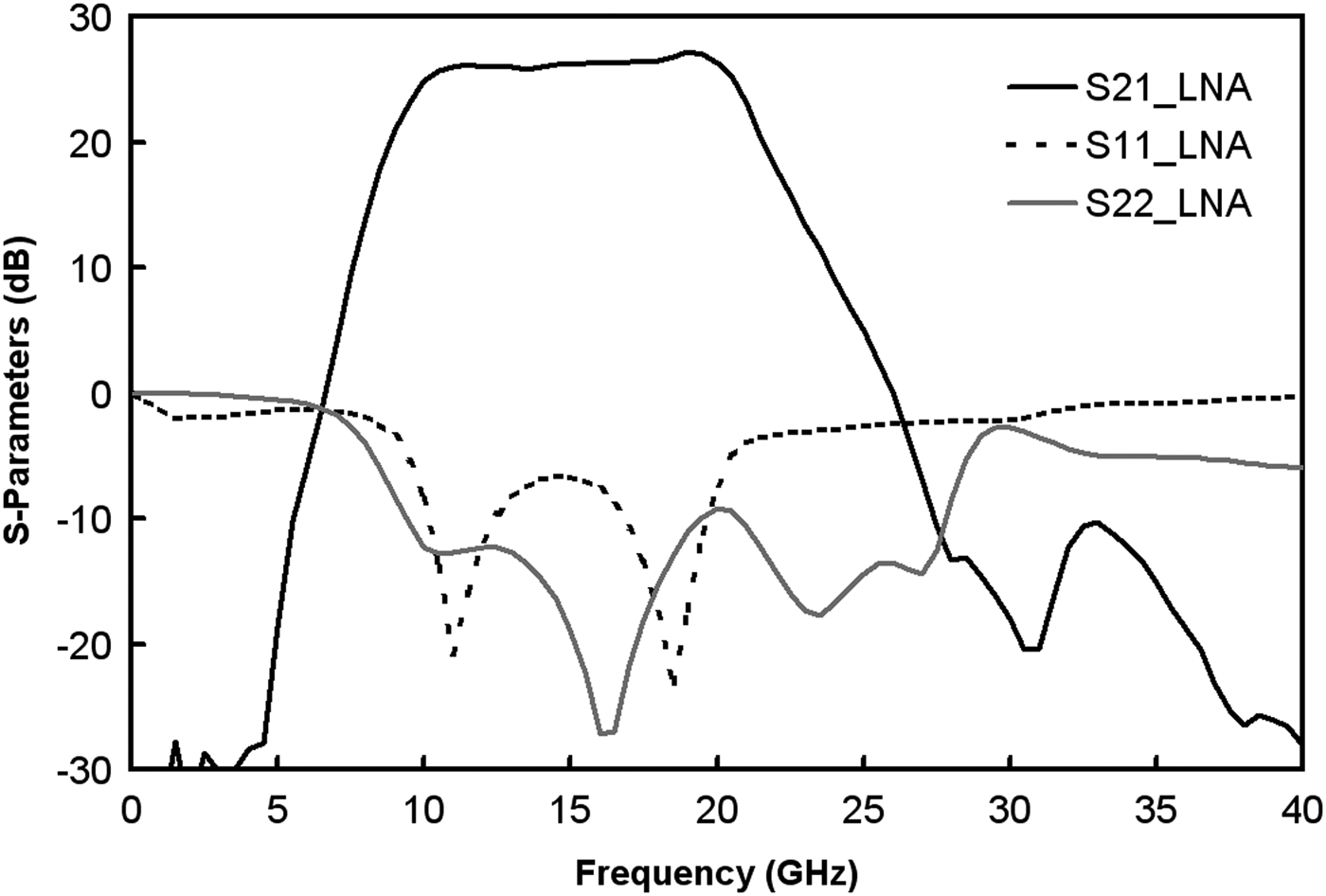
Figure 5 shows the broadband S-parameters measurements (DC–40 GHz) of the amplifier in LNA biasing condition (VD3 = 1.75 V).
Fig. 5. DC-40 GHz measurements of amplifier S-parameters – “LNA” biasing mode.
Measurements are close to the expected simulated results: flat gain in the operating bandwidth (lower than 0.9 dB over 12–19 GHz frequency range) and wideband output matching (lower than –11 dB over 10 GHz bandwidth).
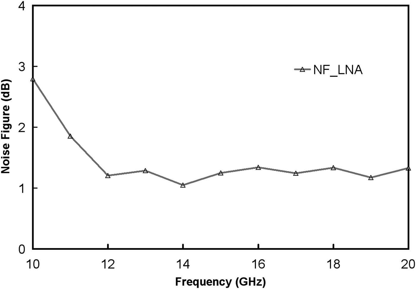
The noise figure, shown on the next figure, is better than 1.35 dB in the full 12–19 GHz frequency range. This result is very interesting in Ku/K band with a process dedicated to power application and validates our flexible strategy design (Fig. 6).
Fig. 6. Amplifier noise figure.
B) Flexibility with biasing modes
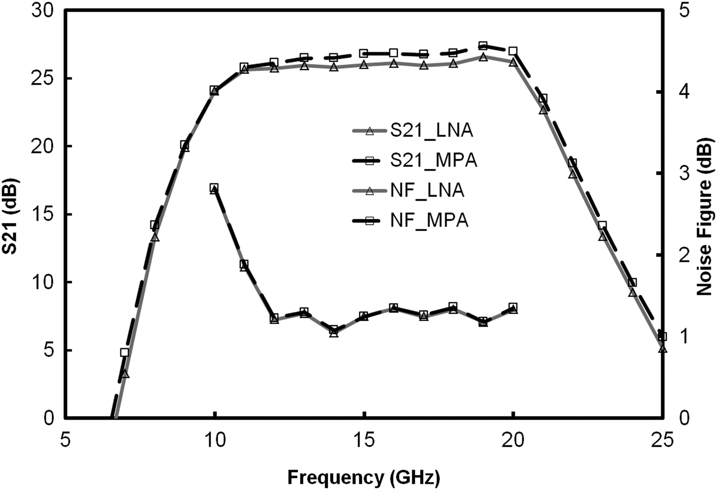
In Figs 7 and 8, gain and noise figure measurements are presented in order to assess a comparison between the “LNA” biasing mode and the “MPA” biasing mode (VD3 = 4.8 V). Figure 7 shows that for both applications the noise figure is unchanged and that the gain variation remains very low (about 0.8 dB worst case).
Fig. 7. Amplifier gain and noise figure for LNA and MPA biasing modes.
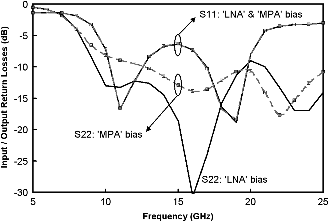
Fig. 8. Amplifier input/output return losses for LNA and MPA biasing modes.
Figure 8 shows that input matching impedance is not sensitive to the different biasing modes. The output return loss remains better than –10 dB worst case.
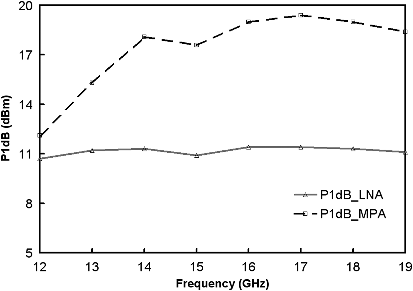
Power measurements have been performed to evaluate the MMIC linearity performances. The next figure presents P1 dB of the amplifier over the operating bandwidth in case of LNA and MPA biasing modes (Fig. 9).
Fig. 9. Amplifier linearity for LNA and MPA biasing modes versus frequency.
The level of P1 dB in LNA biasing mode is constant, around 11 dBm, over the bandwidth. Considering MPA biasing, P1 dB is higher than 17.5 dBm in 14–19 GHz frequency range. The diminution of P1 dB in 12–14 GHz frequency was predicted by simulation; it is due to a compromise between linearity, output impedance matching and gain flatness.
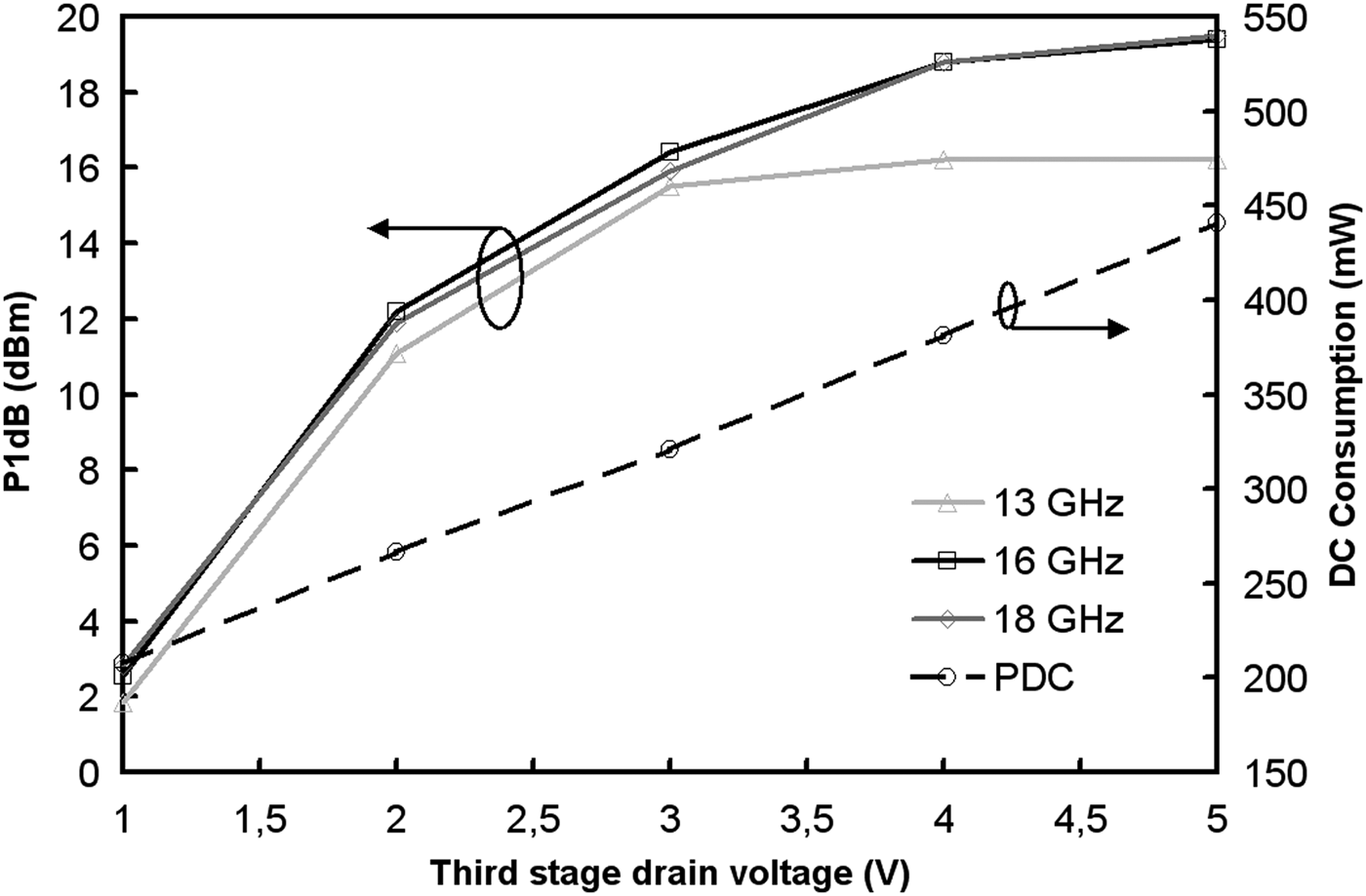
Measurements of P1 dB and DC consumption versus output stage drain voltage have also been performed. Indeed, a linear increase of DC consumption does not lead to a linear augmentation of linearity. Therefore, Fig. 10 permits to choose the best compromise linearity/DC consumption following required specifications.
Fig. 10. Linearity and DC consumption versus third stage drain voltage.
These measurements allow us to conclude that the biasing conditions of the third stage have no impact on the small-signal RF behavior of the MMIC. Modifications concern therefore only the linearity/DC consumption ratio. This result constitutes a key point of flexibility aspect. Indeed, a modification of polarization mode in RF equipments permits to change the setting of linearity or DC consumption without impact to the noise figure, the gain, the gain flatness and return losses.
C) Manufacture and technology dispersion
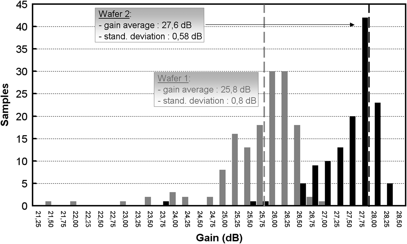
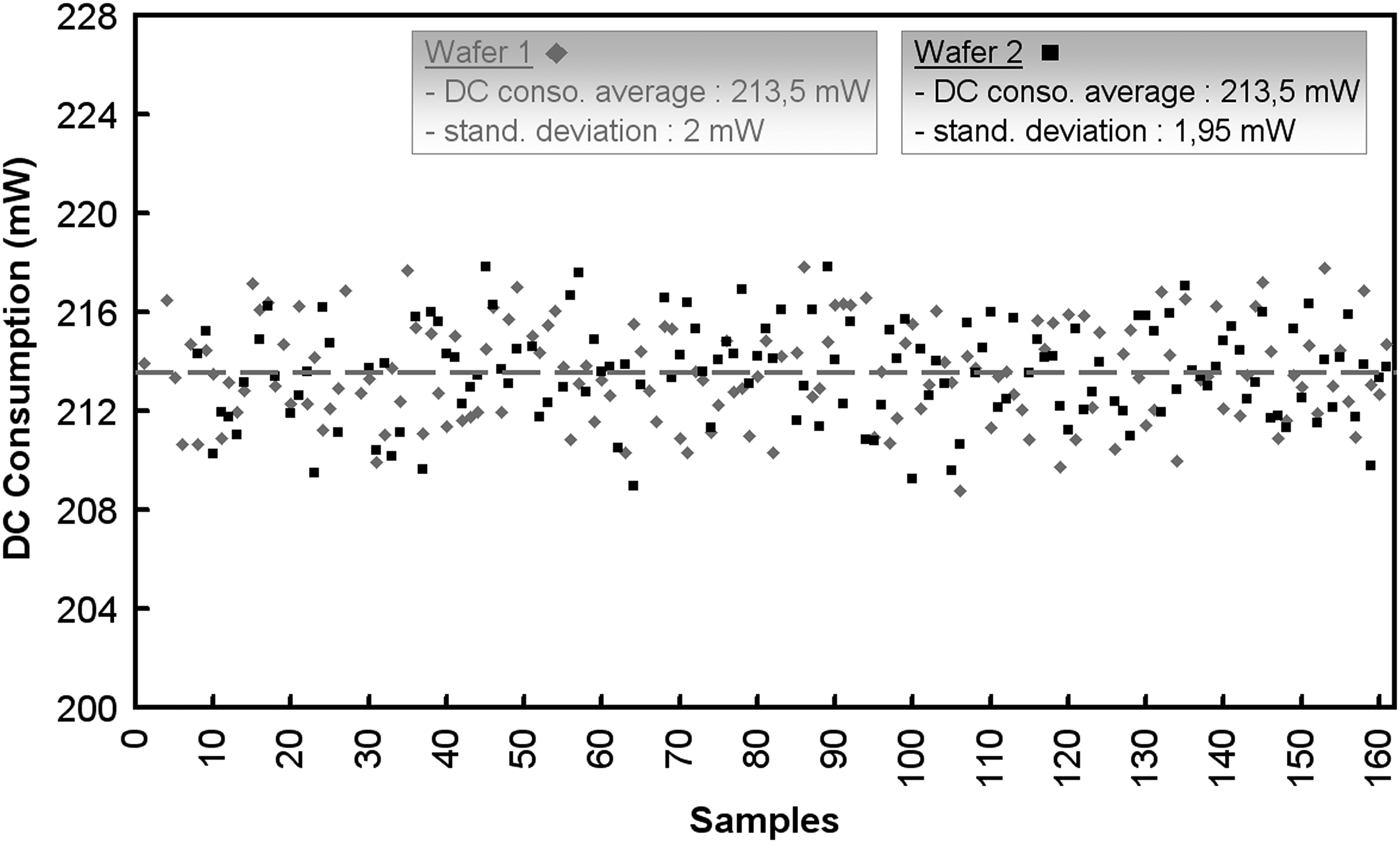
Two wafers have been manufactured by OMMIC. All the MMICs have been measured on-wafer. The electrical yield is 92% on the first wafer and 77% on the second. Figure 11 shows the gain performance of all functional chips for both wafers. The analysis of the gain dispersion at 16 GHz (center of operating bandwidth) presented in Fig. 12, indicates that gain average is higher for the second wafer (27.6 versus 25.8 dB). But the standard deviation of the two wafers remains weak: 0.58 dB (wafer 2) versus 0.8 dB (wafer 1). Moreover, the DC consumption dispersion of the two wafers, shown in Fig. 13, allows us to observe that the average is the same (213.5 mW in LNA biasing mode) and that the weak standard deviation is similar (about 2 mW).
Fig. 11. Gain beam of functional chips on two wafers.
Fig. 12. Gain dispersion of two wafers.
Fig. 13. DC current dispersion of two wafers.
Performance variations on the same wafer are low and the behaviors of all functional MMICs are quite similar. D01PHS process dispersion seems to be reduced, due to the etch-stop layer included in the epitaxy. Those results confirm that this technological process is suitable for space applications where several equipments have to be duplicated.
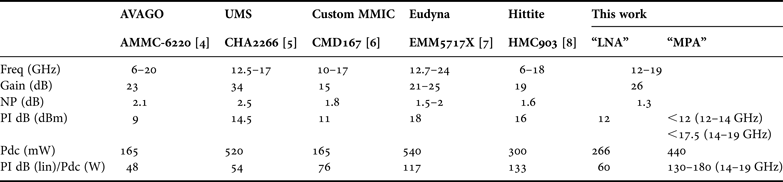
D) Comparison with other commercial off-the-shelf (COTS)
A comparison between this work and COTS is summarized in Table 1. The criterion: P1 dB (in linear)/Pdc (W) is defined in order to evaluate the performance. The MMIC presented in this paper is able to compete with HMC903 following this criterion, and it presents a better noise figure. Moreover, thanks to flexibility capabilities, this MMIC is able to satisfy the LNA need: low noise associated to reduced DC consumption.
Table 1. Comparison between MMIC and COTS.
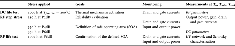
V. FUTURE WORKS: D01PHS RELIABILITY ASPECTS
Before to obtain the permission to flight, each European components and technologies have to be qualified and capability approved to the rules of the ESCC Specification System and the results certified by ESA.
Today, D01PHS process is not included in this EPPL (European Preferred Parts List) components. In the continuation of the design, realization and characterization of the amplifier, the space qualification of this technology will be the next step of this work.
Several measurements, listed in Table 2, will be performed on RF and DC parameters of the amplifier before the start of the stress (T 0), at the middle of the stress (T mid) and at the end (T end). Following the drifts observed on these parameters, D01PHS process could be considered space qualified.
Table 2. Test plan.
VI. CONCLUSION
In this paper, the design and the characterization of a wideband three stages amplifier has been presented. This MMIC, manufactured by OMMIC, is an LNA in 12–19 GHz frequency range (noise figure lower than 1.35 dB) and a linear amplifier by using different third stage polarization setting (flexible P1 dB up to 19 dBm). The interest of this topology is, following the requirements, that linearity/DC consumption ratio is adjustable during a mission without impact on the others RF performances (noise figure, gain, flatness, and return losses).
D01PHS is the chosen process due to the low-noise and linear capabilities but also because this process permits to limit the technology dispersion thanks to a specific etch-stop layer. Now, the second part of this study, dedicated to the space qualification of this process, will start. Following the reliability tests, D01PHS will be included in the EPPL.
ACKNOWLEDGEMENTS
The authors acknowledge ESA, in charge of ECI program, for financial support and OMMIC for the wafer manufacturing and for MMIC on-wafer measurements.
François-Xavier Estagerie was born in Brive (France) in 1981. He received the Ph.D. degree in Electronics from the University of Limoges in 2007. He joined the Thales Alenia Space company, France, in 2007 as microwave product design engineer. Since 2010, he is MMIC design engineer and developed a variety of MMIC functions (low-noise and linear amplifiers, mixers, etc.).
Dominique Langrez was born in France, in 1966. He received the Ph.D. degree in electronics from University of Science and Technology of Lille, Lille, France, in 1996. In December 1996, he was an R&D Microwave Engineer with the MMIC Design Department of Alcatel Alenia Space, Toulouse, France, where he was involved in the designing of Monolithic Microwave Integrated Circuits for telecommunication applications encountered in radio links, Earth-based stations, and payload satellites. He is currently the Head of the MMIC & RF Reliability Group of the Microwave Product Line at Thales Alenia Space – France.
Jean-Luc Muraro received his Ph.D. degree from the Université Paul Sabatier in Toulouse in 1997 for his research into the reliability of Solid-State Power Amplifiers. He has joined Thales Alenia Space in 1997. Actually he is the Head of the Microwave Reliability Laboratory. He is the in-charge of the Space Qualification Program for MMICs and is currently researching reliability aspects of new technologies including wide band gap power amplifiers, MEMS devices, and non-hermetic packaging for space applications. He authored or co-authored 60 technical papers in various journals or conferences.
Jean-Louis Cazaux was born in 1960. He got his Ph.D. degree in Physics and Electronics in Toulouse in 1985, then was Post-Doc research fellow at University of Michigan, Ann Arbor, USA in the field of advanced transistors and circuits for microwave electronics. In December 2003 he obtained a Habilitation (for Researches Steering) from Université Paul Sabatier, Toulouse. He joined Alcatel Space in 1988 as MMIC (Microwave Monolithic Integrated Circuit) designer. From 1996 to 2012, he was the head of the Microwave Advanced Studies within the Microwave Department of what is now Thales Alenia Space. Since Jan. 2013, he acts as Technology Manager for the Competence Center Electronics of Thales Alenia Space – France. He represents Thales Alenia Space at the EuRAMIG (European Microwave Interested Group) meetings. He represents EUROSPACE, in behalf of Thales Alenia Space, at the SCSB (Space Component Steering Board) and at the Plenary CTB (Component Technology Board) two bodies of the ECSS (European Space Components Coordination) led by European and National Space Agencies. In 2006, he founded AXIS, a Research Joint Lab between his company and XLIM-University of Limoges, for which he acted as co-Director since that date. He authored or co-authored 300 technical papers in journals or conferences and holds 6 technical patents. He acts as reviewer and expert for the European Commission (FP7) and the French ANR (VERSO in 2008/9) and AERES. He belonged to the Board of Director (BoD) of the European Microwave Association in 1999/2002 (representing France) and in 2010/2012 (representing Industry). He was the French representative at the General Assembly of EuMA (2003/06), to the Technical Com. of EuMC, of French JNM (Journées Nationales Microondes), and of MEMSWAVE Conference. He was co-editor of one special issue of the Proceedings of EuMA. He was the Chairman of the European Microwave Conference 2005 (Paris). He is an editor of the Int. Journal of MWT.
Rémy Leblanc was born in Paris (France) in 1959. He received the Engineer degree from the “Telecom-ParisTech” High School in 1983. After graduation, he worked with the microwave research group of the Laboratoire d'Electronique PHILIPS, where he was involved in MMIC design and modeling. Between 1988 and 2000, he has been Manager of the Foundry Support Group within the Philips Microwave Limeil GaAs Foundry. Between 2000 and 2010, he has been Manager at OMMIC of the MMIC Design, Product Engineering and Foundry Support activities. Since 2011, he is Director of Product Development, including MMIC Design, Foundry Support, Qualification and Reliability activities.