


Introduction
Frequency selective surfaces (FSS) over the last decade are drawing considerable research attention due to their wide range of applications as spatial filters that can be used for selective transmission of specific frequency band while rejecting the others [Reference Munk1] in the domain of microwave and millimeter wave. Designs of multiband FSS have been intensively investigated due to the great demand of multiple independent transmission bands in wireless communication systems. In case of low frequency, closely located, narrowband operations like Wi-Fi, WIMAX, and WLAN, miniaturization of element size and reduction of frequency ratio (FR) are becoming a major concern. Several approaches regarding dual, tri or quad band FSS design [Reference Li and Cao2–Reference Parker, Robertson, Sanz-Izquierdo and Batchelor12] have been reported so far in earlier literatures. Substantial amount of work has also been reported [Reference Liu, Sheng, Fan and Guo4–Reference Kartal, Golezani and Doken16] in the accomplishment of multiband FSS design.
To achieve multiple pass bands or stop bands with sufficient reduction in cell dimension and to obtain adjacent band FR with better angular stability, cascaded FSS designs with two or more metallic array are extensively reported in early works [Reference Li and Cao2–Reference Yan, Wang, Ma, Qu, Zhang, Xu, Zheng and Zhang7]. Cascading of complementary meandered structure with complementary grid structure [Reference Li and Cao2] and a combination of complementary structures with spatial lumped element [Reference Wang, Chang, Che, Chin and Chow3] have been investigated for dual layered tri-band application. Similarly, four branch spiral triangle, when convolved with gridded tortuous cross-dipole, three closely spaced bands can be obtained [Reference Liu, Sheng, Fan and Guo4]. A new triple-layered FSS is realized for tri-band GSM application [Reference Doken and Kartal5]. Moreover, multilayered fractal structure design provides X band application of FSS [Reference Li, Li, Zhang and Zhao6]. Another triple layer cascading technique involves two gridded triple square loop array cascaded with double square loop [Reference Yan, Wang, Ma, Qu, Zhang, Xu, Zheng and Zhang7] resulting in highly selective quad band responses. However, the thicknesses of the aforementioned structures are too large to make the FSS suitable for practical applications. Such types of design optimization also suffer from the undesired mutual effect between each layer.
The ultra-thin single metallic sheet without any dielectric substrate may also provide quad band response [Reference Rahmati and Hassani8]. A unit cell of that FSS has four square slots within which multiple stubs are loaded to provide close amount of band spacing. In another approach, close dual or tri-band response can be achieved by using three concentric split rings slots [Reference Fabian-Gongora, Martynyuk, Rodriguez-Cuevas and Martinez-Lopez9–Reference Fabian-Gongora, Martynyuk, Rodriguez-Cuevas and Martinez-Lopez10]. Closely packed concentric circular slots with narrow metallic short can redistribute the surface current that in turn minimizes the coupling effect upon which effective reduction in large band separation can be achieved. Another single layer ultrathin structure provides close dual band response for X band application where FSS unit cell is composed from centered square patch with L shaped arms [Reference Unaldı, Cimen, Cakır and Ayten11]. The above literatures [Reference Rahmati and Hassani8–Reference Unaldı, Cimen, Cakır and Ayten11] reveal the mechanism to obtain close spaced multiband using single layer FSS due to their higher resonance frequency. However, effective cell miniaturization has not been confirmed yet. The miniaturization of cell size is another major issue for multiband FSS due to its wide employability in electromagnetic shielding for indoor communication [Reference Parker, Robertson, Sanz-Izquierdo and Batchelor12]. The miniaturized crooked cross convoluted geometry has been discussed for single layer FSS with dual closely space bands [Reference Sivasamy and Kanagasabai13]. In another work [Reference Ghosh and Srivastava14], a dual closely located stop band FSS with better miniaturization has been reported where the FSS comprises two convoluted meandered metallic strips in each quadrant of the unit cell connected through a cross dipole. Another miniaturized dual band FSS unit cell design has been evolved from conventional patch slot topology [Reference Wdew, Riaz, Naeem and Shafique15].
In this paper, a miniaturized single layer five band FSS is presented. The miniaturized FSS unit element size is 0.065 λ o1 × 0.065 λ o1 large and 0.21 λ 05 × 0.21 λ 05 large where λ 01 and λ 05 stands for the wavelength for lower and higher operating band. The metallic layer of unit cell geometry consists of six concentric octagonal narrow strips where adjacent octagonal metallic loops are interconnected to each other. In addition to this, four arrow-shaped meandered strips has been connected to the outer most loop. Employing the interconnection technique between the adjacent loops, 44% cell size reduction can be accomplished. Furthermore, increasing the effective electrical length of the proposed cell by incorporating arrow-shaped meandered line, 23% cell reduction has also been achieved. Besides, the substrate thickness in the proposed structure has been noticeably reduced by 45% due to the extremely thin dielectric material employed here. In addition, an impressive reduction in frequency band ratio has been observed where the minimum value is as low as 1.22. The proposed FSS can be utilized as a special kind of Band Stop Filter, which can be applicable in Wi-Fi, WLAN, and X band downlink satellite service.
Development of unit cell structure and simulated results
The proposed five band structure has been illustrated in Fig. 1. This proposed unit cell structure is derived from basic octagonal concentric sequential loop design with symmetrical arm length. Figure 2 illustrates step by step development to finalize the ultimate proposed structure. Each individual octagonal metallic strip acts as a resonating arm and its effective length is approximately λ/2 corresponding to the resonance. Besides the inductive loading of concentric octagonal patterns, another influencing factor is the uniform narrow spacing between adjoined metallic loops which causes strong capacitive effect. By exploiting the coupling mechanism and introducing the sixth concentric loop, a significant resonance shift towards lower frequency band (especially for the fifth band) can be achieved. As a result of that indicative reduction of unit cell dimension multiple to λ 05 occurs, where λ 05 is the wavelength corresponding to the fifth resonant frequency. However, due to the sequential coupling effect, slight shifting of first four resonant frequencies towards higher frequency range can be observed. Interactive coupling also reduces the FR between adjacent bands. In the next development, four beveled arm of the exterior octagonal strip connected to four symmetrical arrow-shaped printed metallic patterns. Meandered arrow-shaped patterns accommodate larger resonance length in smaller area which further increases the inductive effect. Captative effect due to enclosed space by arrow-shaped metallic ring also increases total capacitance value. As a result of that, better shifting of first resonance towards the lower frequency band can be observed as illustrated in Fig. 3 and Table 1. On the other hand, minor or negligible shifting can be observed for the other four resonances towards the lower frequency range. Unit cell also reduces from 0.154 λ 01 to 0.118 λ 01 where λ 01 is the wavelength corresponding to the lower resonant frequency. Adjacent band ratio f 2/f 1 is considerably high because of the large resonance shifting of the first band compared to the second one. In the final development, neighboring loops are interconnected with each other with the help of narrow metallic conductors having a similar width. The proposed gridded loop structure is basically a meandering pattern with large effective electrical length which connects ad joint octagonal resonating elements and therefore produces a noticeable improvement for equivalent inductance and capacitance for all five resonant. Resonating arms for each stop band resonance are in sharing mode of the proposed meandered pattern. As shown in Fig. 4 it is observed that transmission zero shifts nearly from 18 to 22% corresponding to the first to fifth resonance with the variation of meandered gap d. Optimized dimension of the designed unit cell are given in mm: L = 8.46, p = 8.2, W = 0.3, D = 0.3, S = 0.3, h = 0.2 and the simulated results have been obtained by using CST microwave simulator. According to the analogy of transmission line theory, for a given length equivalent capacitance will be smaller for the wider gap between two parallel metallic strips. By varying gap width in between metallic strips, capacitive effect can be reduced which further increase the resonating frequencies.

Fig. 1. Unit cell geometry of the proposed five band FSS.

Fig. 2. Sequential development of unit cell. (a) Configuration-1 (five concentric octagonal loops). (b) Configuration-2 (six concentric octagonal loops). (c) Configuration-3 (six concentric octagonal loops with four arrow-shaped rings without interconnection). (d) Proposed configuration.

Fig. 3. Transmission response of different configuration. (a) Configuration-1. (b) Configuration-2. (c) Configuration-3. (d) Proposed configuration.

Fig. 4. Variation of transmission response with different “d”.
Table 1. Development of proposed configuration

Surface current analysis
To understand the significant resonance frequency shift towards the lower frequencies, surface current distribution analysis has been demonstrated and explained. Figure 5(a) illustrates the surface current distribution for concentric octagonal loop without interconnection and Fig. 5(b) shows the surface current distribution proposed interconnected concentric octagonal loop element at different resonance frequencies. The monopole like current distribution can be observed for all the five resonance frequencies, if the adjacent octagonal loops are not interconnected with each other. Without interconnection, physically five individual loops are mainly responsible for the respective five resonances. Although the mutual coupling effect of the adjacent loop can also be seen due to the closer gap of successive loops, major responsibility lies on the individual loop and the effective surface current path is approximately equivalent to the quarter wavelength of its corresponding resonant frequency. As an example, the current distribution at 4.32 GHz can be seen especially along the outermost loop and arrow-shaped rings; similarly, the surface current at 22.51 GHz is mainly concentrated around the fifth ring. The minor current concentration to the adjacent ring occurs due to the mutual effect of the adjacent ring. On the other hand, intentional interconnection between adjacent loops demonstrates dipole like surface current distribution. Impressive improvement of the traveling current path can be clearly observed for each resonant frequency in Fig. 5(b). An enlargement of effective current path which is approximated to half-wavelength at its corresponding frequency makes remarkable enhancement of equivalent inductance. Larger equivalent inductance leads to lowering of resonance frequencies. Thus, the smaller element size is achieved. Without interconnection between the adjacent concentric loops, there will be a strong interaction among the vertical surface currents at the narrow capacitive spacing between two adjacent metallic strips. Due to this strong mutual coupling, the adjacent frequency band shifts away. Consequently, the higher FR between the adjacent bands can be observed. However, in proposed cell geometry, asymmetrical current distribution reduces the coupling effect between the adjacent loops, causing the close band-spacing.

Fig. 5. (a)Surface current distribution for different frequencies without interconnection. (b) Surface crrent distribution for different frequencies with interconnection.
Furthermore, evaluating the surface current for each resonant frequency, an equivalent circuit model can be realized. The surface current at 2.4 GHz is mainly concentrated on the three outermost loops as shown in Fig. 5(b) through the interconnection. Excited surface current of the parallel lines are oppositely directed thereby forming a series connection. Interconnection produces length enhancement of effective meandered pattern which further increases the effective inductance. The closer gap between adjacent metallic loops produces a strong coupling effect which produces a large capacitive effect and consequently lowers the resonant frequency. Similarly, at 3.38, 4.82, 6.32, and 7.75 GHz impressive improvement of inductive length occurs due to the interconnection of successive inner loops
Equivalent circuit extraction and analysis
The proposed lumped equivalent model has been represented by a series LC circuit, with characteristics impedance z 0, across the transmission line for all the five resonant frequencies as shown in Fig. 6. As it is hard to realize an accurate model of the proposed complex FSS structure, an estimation of the lumped parameters like inductance (L) and capacitance (C) from the proposed structure becomes a challenging problem. However, adopting the hypothesis of approximate structural equalization between symmetrical octagonal strip and circular ring conducting loop [Reference Ramezani Varkani, Hossein Firouzeh and Zeidaabadi Nezhad17] and exploiting the surface current analysis from Fig. 5 for each resonance frequency, adequate synthesis and simplified formulation of circuit elements can be provided with fair level of accuracy.

Fig. 6. Equivalent circuits of FSS. at (a) 2.4 GHz. (b) 3.38 GHz. (c) 4.82 GHz. (d) 6.32 GHz. (e) 7.75 GHz.
In this paper, the equivalent circuit analysis has been organized in two sections. The first section comprises synthesis procedure of L-C equivalent circuit from the desired filtering response as depicted in Fig. 6. The subsequent section offers a relationship between the equivalent circuit parameters and the physical dimension of the proposed FSS.
Synthesis of the Effective L–C circuit model of the proposed microwave filter can be done by exploiting the contiguous surface current distribution. In early synthesis, it is assumed that the octagonal strips are independent without any metallic short and thereby the effective inductance (L 1–L 6) can be approximated to be proportional to the corresponding octagonal conductor length (X 1–X 6). Further, the successive loop interconnection providing the inductive nature of metal short produces a meandered strip line and the series connection between successive inductors. On the contrary, capacitance (C 1–C 6) of the circuit model which completely depends on the width of gap between the conducting strips and neighboring unit cell, forms parallel connection. To simplify the analysis, mutual coupling between the metallic strip and capacitive effect inside the arrow-shaped ring resonators as well as the capacitive gap between the meandered line have not been considered.
Since for each stopband resonance frequency, inductance enhances due to the enlargement of the metallic pattern, the meandered line has profound effects on capacitance as illustrated and as well explained in surface current distribution analysis. Therefore, the resonant frequencies of five stop bands can be roughly expressed as
 $$f_{r1} = \displaystyle{1 \over {2{\rm \pi} \sqrt {\lpar {L_1 + L_2 + L_3} \rpar C_{eq1}}}}, $$
 $$f_{r2} = \displaystyle{1 \over {2\pi \sqrt {\lpar {L_1/4 + L_2 + L_3 + L_4/4} \rpar C_{eq2}}}}, $$
 $$f_{r3} = \displaystyle{1 \over {2\pi \sqrt {\lpar {L_3 + L_2/2 + L_4/2} \rpar Ceq_3}}}, $$
 $$f_{r4} = \displaystyle{1 \over {2\pi \sqrt {\lpar {L_4 + L_3/2 + L_5/2} \rpar Ceq_4}}}, $$
 $$f_{r5} = \displaystyle{1 \over {2\pi \sqrt {\lpar {L_4 + L_5 + L_6/2} \rpar Ceq_5}}}, $$
where different sets of effective inductances (L 1–L 6)and capacitance (C eq1–C eq5) values have been shown in equation (1)–(5) corresponding to the resonant frequencies.
The equivalent capacitor is the sum of capacitive effect of the gap between successive octagonal rings. Using the surface current distribution analogy Equivalent capacitance C eq1–C eq5 may be expressed as
 $$C_{eq1} = C_1 + C_2 + C_{3\;}, $$
 $$C_{eq2} = C_2 + C_3 + C_4,$$
 $$C_{eq3} = C_3 + C_4,$$
 $$C_{eq4} = C_4 + C_5,$$
 $$C_{eq5} = C_5 + C_6.$$
Multiple simulations have been performed in ADS to extract the values of L and C which can be derived as: L 1 = 21.02 nH, L 2 = 12.6 nH, L 3 = 8.37 nH, L 4 = 7.6 nH, L 5 = 6.4 nH, L 6 = 3.2 nH, C eq1 = 104.5 fF, C eq2 = 79 fF, C eq3 = 59.1 fF, C eq4 = 44.1 fF, and C eq5 = 27.1 fF. It can be found that weakening of the capacitive effect corresponds to the higher frequency because of the descending gap circumference among inner conductor loops.
Next section deals with the mapping between equivalent circuit model parameters and physical dimension of the proposed FSS structure where the selection of octagonal loop structure is the best compromise between the circular loop [Reference Ramezani Varkani, Hossein Firouzeh and Zeidaabadi Nezhad17] and the straight-line square loop [Reference Langley and Parker18–Reference Yang and Shen20]. The development of the proposed design comprises the following steps. Initially, six concentric octagonal loops have been designed. In the next step, as four slant arms of outermost loops are interconnected with four triangular loops, an enlargement of outer periphery in limited space of unit cell occurs a significant phenomenon occurring in case of the circular equivalent polygon structure. Finally, adjacent octagonal rings are interconnected with each other. The parameters of the proposed interconnected loop structure are listed in Table 1. In order to map the equivalent circuit model parameters to the physical dimension of proposed unit cell structure, Marcuvitz modeling technique for periodic array of thin conducting strip has been used [Reference Langley and Drinkwater21]. To estimate the equivalent inductance and capacitance of the concentric octagonal loop-shaped FSS structures, following basic equations [Reference Ramezani Varkani, Hossein Firouzeh and Zeidaabadi Nezhad17] have been used:
 $$\eqalign{L_1\omega _r & = 2 \times \displaystyle{{6X_1} \over p} \times \displaystyle{{F\lpar {\,p,d,\lambda} \rpar .F\lpar {\,p,d,\lambda} \rpar } \over {F\lpar {\,p,d,\lambda} \rpar + F\lpar {\,p,d,\lambda} \rpar }} \cr &= \displaystyle{{12X_1} \over p} \times \displaystyle{{F\lpar {\,p,d,\lambda} \rpar } \over 2}\;} $$
 $$L_2\omega _r = \displaystyle{{4X_2} \over p}F\lpar {\,p,2d,\lambda} \rpar ,$$
 $$L_i\omega _r = \displaystyle{{4X_i} \over p}F\lpar {\,p,2d,\; \lambda} \rpar ,,$$
 $$\eqalign{C_1\omega _r &= 0.75 \times 4 \varepsilon _{eff}F{\rm (}p,g_a,\lambda {\rm )} \times \displaystyle{{3X_1} \over p} \cr & = \displaystyle{{9X_1} \over p} \varepsilon _{eff}F{\rm (}p,g_a,\lambda {\rm )},} $$
 $$C_2\omega _r = \displaystyle{{2X_2} \over p}4\varepsilon _{eff}\displaystyle{{F\lpar {\,p,g_a,\lambda} \rpar .F\lpar {\,p,g_a,\lambda} \rpar } \over {F\lpar {\,p,g_a,\lambda} \rpar + F\lpar {\,p,g_a,\lambda} \rpar }},$$
 $$C_i\omega _r = \displaystyle{{2X_i} \over p} \times 4\varepsilon _{eff} \times \displaystyle{{F\lpar {\,p,s,\lambda} \rpar .F\lpar {\,p,s,\lambda} \rpar } \over {F\lpar {\,p,s,\lambda} \rpar + F\lpar {\,p,s,\lambda} \rpar }} = 8\displaystyle{{X_i\varepsilon _{eff}} \over p} \times \displaystyle{{F\lpar {\,p,s,\lambda} \rpar } \over 2},$$
where εeff, F, D, p, d, s, and g a correspond to the effective dielectric permittivity of the media, correction factor for the associated inductance and capacitance, size of the unit cell, gap between the outer loop parallel arm, width of the octagonal metallic strip, gap between successive loops, and effective gap of the unit cell, respectively. The quantity g a = D–p whereas X 1 and X 2 denote the arm length of most exterior and second most exterior arm length, respectively, X i is the arm length of successive octagonal loops with i = 3, 4, 5, 6.
One arrow-shaped structure perimeter has been considered to be one arm length of X 1.
Angular stability
Figure 7 illustrates transmission coefficient of the proposed FSS for TE and TM polarization under various oblique indent angles. It can be observed that under the large variation of incident angle (0° ≤ θ ≤ 60°) at a step of 20°, stop bands for TE polarization deviate slightly as 0.4, 0.26, 0.38, 2.27, and 2.45%, respectively. On the other hand, TM polarization deviations are 1.2, 1.9, 1.3, 2.1, and 2% corresponding to the five successive stop bands. However, still the proposed FSS provides acceptable resonance deviation <2.5% within the allowable limits. Bedsides bandwidth of TE waves slightly increases whereas bandwidth of TM wave decreases with respect to the increment of incident angle from 0° to 60°. These changes are mainly caused by variation of wave impedance as discussed in [Reference Cimen22].

Fig. 7. Simulated transmission coefficient of proposed FSS structure under different incident angle. (a) TE polarization. (b) TM polarization.
Experimental verification
To validate the simulated results of proposed structure, a prototype has been fabricated on FR-4 substrate having relative permittivity ε r = 4.4, loss tangent tanδ = 0.02, and thickness h = 0.2 mm. prototype dimension is 320 × 320 mm2, containing 38 × 38 elements as shown in Fig. 8. Transmission coefficient measurement of fabricated FSS has been carried out using two horn antennas connected to network analyzer (Rohde & Schwarz ZND20). a relatively good agreement between simulated and measured result has been observed in Fig. 9. Free space measurement setup is shown in Fig. 10. Two types of horn antennas pair has been used sequentially. Initially, large size Horn Antenna pair is used with frequency handling capacity of 2–3 GHz. Another Horn Antenna pair with operating frequency range 3–8 GHz used in next measurement. Due to the ultra-thin and flexible nature of the proposed prototype as observed in Fig. 10(c), prototype is attached carefully with the air foam sheet for measurement support. Moreover angular stability have been validated for the proposed structure. Transmission coefficient S 21 of the different oblique incident angle at θ = 0° and θ = 30° have been carried out. Figure 11(a) shows TE polarization variation of the structure Fig. 11(b) shows TM polarization variation of the proposed structure. Both experimental responses show its parity with simulated results for both the angles.

Fig. 8. Photograph of fabricated FSS prototype.

Fig. 9. Simulated and measured S-parameter under normal incidence.

Fig. 10. (a) and (b) Experimental setup in free space (c) colded prototype.
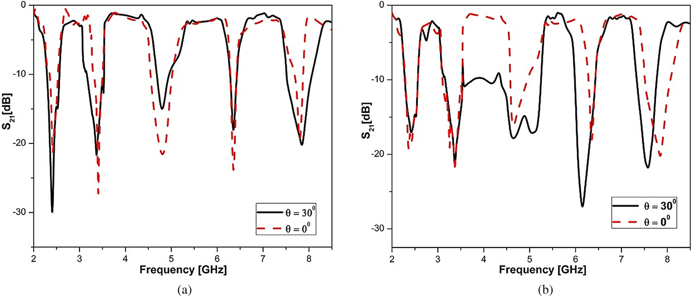
Fig. 11. Measured polarization (a) TE and (b) TM in different angles..
Conclusion
A new miniaturized ultrathin FSS with five closely spaced stop bands is investigated numerically and experimentally. Adjacent loop interconnection technique is illustrated and demonstrated through the developed benchmark design. The proposed design has shown a convenient way to achieve five band FSS with multiple distinctive features such as compact (0.0656 λ 0 × 0.0656 λ 0) unit cell and ultra-thin thickness of 0.0016 λ 0 at lower resonant frequency. Adjacent band ratio of five bands is also settled in close range with minimum value of 1.22. The frequency characteristics have been extensively analyzed by equivalent circuit model and surface current analysis. Table 2 confirms the excellence of the proposed design with some other multiband FSS design irrespective to the number of resonant frequencies, unit cell size miniaturization, and dielectric thickness reduction. In addition to these significant achievements, the proposed structure provides stable transmission performance under oblique incidence of 60° for both TE and TM polarization. Finally, a prototype has been fabricated and tested which exhibit satisfactory agreement with the simulated result.
Table 2. Comparison with existing multiband FSSs

 Mr. Anupam Dey received his B.TECH and M.TECH degree in Electronics and Communication Engineering from WBUT in 2010 and 2014, respectively. Presently, he is working as an Assistant Professor in ECE department in Calcutta Institute of Technology, Howrah, West Bengal His main research interests are design and optimization of Microstrip Antenna and Frequency Selective Surfaces.
 Mr. Rajarshi Sanyal has obtained his AMIETE and M.Tech. Degree in Electronics and Communication. His area of Research Includes Microstrip Antenna and Microstrip filters. Presently, he is associated with MCKV Institute of Engineering as an Assistant Professor. He has presented and published various research papers in national and international journals.


