I. INTRODUCTION
A microstrip antenna (MSA) is one of the preferred choices for portable Wireless Communication devices because of its small size, ease of fabrication, and light weight. This is the main reason as to why a lot of research is being carried out in the field of MSA to get a multi-frequency and wideband behavior. The different techniques for getting a wideband behavior that are available in literature include the use of thick substrates [Reference Abdelaziz1], stacked patch antennas [Reference Serra, Nepa, Manara, Tribellini and Cioci2], E-slot patch antennas [Reference Ang and Chung3], patch antennas with defected ground structures (DGS) [Reference Prajapati and Kartikeyena4], T-shaped parasitic strip antennas [Reference Qin5], and metamaterial antennas for gain and bandwidth enhancement [Reference Majid, Rahim and Masri6]. In [Reference Yuehe, Karu and Trever7] authors proposed an E-shaped antenna for wireless local area networks (WLAN) in the 5–6 GHz operation frequency range. In [Reference Kaur, Khanna and Kartikeyena8] authors designed an antenna for multi-band applications covering WLAN, WiMAX, IMT, and Bluetooth applications, the wideband behavior of antenna was due to a monopole antenna with a DGS. Another method for getting broad band behavior is through the use of fractal antenna geometry where regular-shaped slots are cut in the patch to get multi-frequency behavior [Reference Saluja and Khanna9].
To investigate further upon the methods to increase the bandwidth of MSA, in the WLAN, WiMaX, and U-NII bands, a simpler technique that is introduced in this paper is the use of a G-shaped semi-spiral patch with aperture-coupled feeding. The designed antenna has the surface area of 35 × 29 mm2 with outer patch dimensions of 22 × 14.3 mm2, the patch has several slots that are cut in it and together show G-shaped geometry. The main slots that are responsible for showing resonance at 3.6 and 5.3 GHz are L1 having dimensions of 16.3 × 1 mm2 and W4 having dimensions of 13.5 × 0.35 mm2 and the ground layer has an aperture slot with dimensions of 10 × 2 mm2. The multi-frequency behavior of the antenna comes from the design that is followed for this antenna; various resonant slots are cut into the patch to give it a semi-spiral G shape. The slots that are cut into the patch help in producing radiations at two resonant frequencies with high gain. It resonates at two bands namely 3.6 GHz showing an impedance bandwidth 307 MHz and a wideband from 4.98 to 5.599 GHz covering a band of 608 MHz. The energy is concentrated at the top of patch when the antenna is excited using aperture-coupled feeding mechanism. The non-contacting method of feeding the MSA also helps in getting a wider bandwidth as compared with the other contacting methods of feeding MSA [Reference Balanis10].
II. ANTENNA GEOMETRY AND DESIGN
It is well known that the probe feeding and microstrip line method of feeding possess inherent asymmetries and generate higher-order modes, which produce cross-polarized radiations, so non-contacting methods of feeding MSA are preferred usually; moreover using non-contacting methods to feed MSA lead to an increase in the bandwidth of these antennas [Reference Balanis10]. In the aperture-coupled method of feeding MSAs followed in the design presented in this paper (Fig. 1), there is a upper substrate called antenna substrate on which a semi-spiral G-shaped patch is made (layer 1 in Fig. 2(a)). On the upper side of the lower substrate called feed substrate, there is a ground layer that has an aperture slot cut in it, a transverse slot to this aperture helps in achieving higher gain of the antenna (layer 2 in Fig. 2(b)). On the bottom side of this feed substrate, there is a feed network (layer 3 in Fig. 2(c)), this type of feeding method has an additional advantage that no radiation from the feed network will interfere with the antenna's radiation pattern [Reference Pozar11]. Moreover, using a feeding method with aperture coupling to the microstrip feed line in MSA designed on thick substrates gives the designer a choice among a lot of adjustable parameters in the form of aperture length, width, shape, and stub-parameters. If all parameters are judiciously selected, then it might lead to an increase in 70% bandwidth of the antenna as compared with other feeding methods such as probe feeding, edge feeding, and proximity feeding [Reference Grag, Bhartia, Bahl and Ittipiboon12]. This is the main reason for choosing this feeding mechanism for the proposed design in this paper, as for the three proposed frequency bands of wireless applications, we require bandwidths >200 MHz at the center frequency of operation, which cannot be easily achieved with the other feeding mechanisms.

Fig. 1. Detail layered view of the designed aperture-coupled antenna.

Fig. 2. (a) Detailed top view of the patch antenna (layer 1). (b) Top view of the ground layer (layer 2). (c) Bottom view of the lower substrate with feed line (layer 3).
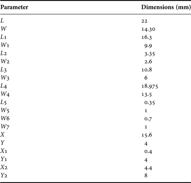
Here in this paper, a semi-spiral G-shaped patch antenna using aperture-coupled feeding mechanism is designed using the transmission line model [Reference Balanis10] and simulated using CST Micro Wave Studio Version 2010 which is a three-dimensional (3D) electromagnetic simulator and its operation is based on the finite integration technique assuming perfect boundary conditions. The detailed geometrical structure of the antenna can be understood from Fig. 2(a), which shows the top view of a semi-spiral G-shaped patch antenna of width W and length L on the upper substrate (layer 1). Various resonant slots along the length and width are cut into the metallic part of the patch, to give it a semi-spiral G-shaped structure, the detailed dimensions of the antenna are presented in Table 1. The main slots that are responsible for showing resonance at 3.6 and 5.3 GHz are L1 having dimensions of 16.3 × 1 mm2 and W4 having dimensions of 13.5 × 0.35 mm2. The antenna is designed on a substrate of dielectric constant 4.4, with loss tangent 0.009 and a thickness of 1.6 mm. Since it is an aperture-coupled antenna, there is one more substrate (lower substrate) of dielectric constant 4.4 with a height of 1.6 mm. The ground plane of the metal that is sandwiched between the upper and lower substrates, has a slot (aperture) of dimensions 15.6 × 4 mm2 that allows feed signals to get electromagnetically coupled from feed line to the antenna and the strength of electromagnetic coupling depends upon the shape and size of the aperture used in the ground (layer 2). There is one more transverse slot to the left-hand side of the aperture slot in the ground, which helps in achieving better impedance matching and improving the output in terms of gain of the antenna. The dimensions of this slot are also mentioned in Table 1. On the bottom of the lower substrate, there is a feed network from where the power flows to the radiating patch. Figure 2(a) represents the top view of the designed patch antenna, Fig. 2(b) represents the top view of the ground plane with an aperture slot and a transverse slot cut in it and Fig. 2(c) represents the view of the feed network, that is, a feed substrate with a feed line.
Table 1. Parametric details of the semi-spiral G-shaped patch antenna, ground layer, and feed line.

The detailed dimensions of the designed antenna are also shown in Table 1. The explicit parameters of the patch (with slots), ground (with aperture and transverse slot), and feed line are mentioned. These are selected using the transmission line model equations mentioned by C.A. Balanis [Reference Balanis10].
III. SIMULATED AND MEASURED RESULTS
A) Return loss
The simulated results in terms of return loss (S 11 in dB), Smith chart, radiation pattern, and impedance matching are shown in Figs 3–7.

Fig. 3. Simulated return loss (S 11 in dB) of the antenna.

Fig. 4. S parameter polar plot of the simulated antenna.

Fig. 5. Smith chart of the simulated antenna matched to 50 Ω.

Fig. 6. (a) E (elevation) plane view of the radiation pattern at 3.6 GHz. (b) H (azimuthal) plane view of the radiation pattern at 3.6 GHz.

Fig. 7. (a) Elevation plane view of the radiation at 5.3 GHz. (b) Azimuthal plane view of the pattern at 5.3 GHz.
Figure 3 shows the plot of simulated antenna's return loss, i.e. S 11 in dB (on the Y-axis) with respect to frequency (on the X-axis). The antenna shows a dual-band behavior at two bands for WLAN/Wi-MaX/U-NII applications at 3.6 GHz (3.432–3.739 GHZ) covering a band of 307 MHz with a return loss of −58 dB, WLAN applications at 5.1–5.3 GHz (4.98–5.597), and U-NII band applications at 5.25–5.35 GHz (4.98–5.597) showing an impedance bandwidth of about 608 MHz and a return loss of −25 dB.
B) Smith chart
It can be seen from Fig. 4 that the simulated Smith chart of the antenna shows a polar plot view of the S-parameters. The respective markers 1, 2, 3, and 4 show the starting and terminating frequencies of the two bands at which the antenna is working. Figure 5 shows the antenna matched to an impedance of 50 Ω.
C) Radiation pattern
The radiation pattern of any antenna is a 3D representation of its radiation characteristics. In order to have a better understanding of antenna's radiation pattern, the elevation and azimuthal plane views of the antenna's radiation pattern in terms of its gain plot are shown in the polar plots in Figs 6(a) and 6(b) at 3.6 GHZ. The designed antenna offers a gain of 4.4 dBi at a resonant frequency of 3.6 GHz. The antenna has a major lobe directed along the broadside direction of radiation at 3.6 GHz.
Figures 7(a) and 7(b) show the radiation pattern plots of the elevation and azimuthal view antenna's radiation pattern at 5.3 GHz. The antenna shows a gain of 4.6 dBi at 5.3 GHz. It has a radiation pattern with two major lobes shifted by 75° with respect to the broadside direction of antenna's radiation.
D) Measurements
The designed antenna was fabricated and then tested using Agilent's Vector Network Analyzer (VNA) E 5071 C series operating in the frequency range from 9 KHz to 8.5 GHz. Figure 8(a) shows the top view of the fabricated antenna (layer 1); Fig. 8(b) shows the ground layer with an aperture slot and a transverse slot (layer 2). Figure 8(c) shows the bottom view of the antenna, i.e. lower substrate with a feed line (layer 3) and Fig. 8(d) shows the assembled antenna with two substrates having patch antenna on the top of upper substrate, feed line on the bottom of lower substrate and ground layer sandwiched between the two substrates.

Fig. 8. (a) Top view of the fabricated antenna. (b) View of the ground layer with slot. (c) Bottom view of the antenna with lower substrate and feed line. (d) Side view of the antenna with two substrates and an SMA connector.
The results of testing the fabricated antenna's return loss on a VNA are shown in Figs 9(a) and 9(b). Figure 9(a) shows the snapshot of VNA when prototype of the designed antenna's measurements are done for return loss and Fig. 9(b) shows the comparison of simulated and measured results.

Fig. 9. (a) Snap shot of VNA during measurement of antenna return loss (S 11). (b) Simulated and measured results of the antenna's return loss (S 11 in dB).
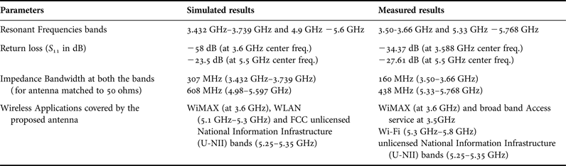
Figure 9(b) shows that the simulated and measured return losses of the antenna are found to be in close approximation with each other (showing about 80% of results matching); this can be verified from Table 2. The resonant frequency at 3.6 GHz has only 0.3% of mismatch with respect to simulated frequency of operation. There is 8% mismatch at 5.2 GHz in terms of frequency of operation and a bandwidth mismatch of 46% for the tested prototype of the designed antenna at 5.2 GHz.
Table 2. Comparison of simulated with measured results.

The measured results are in good agreement with the fabricated ones, but there is a little variation between the simulated and measured results in terms of resonant frequencies of operation and the bandwidth at these frequencies. The variation is mainly because of the errors that are introduced during fabrication of the antenna and the soldering connections of feed cable and the connector.
IV. PARAMETRIC ANALYSIS OF THE ANTENNA
The designed MSA operates in the TE10 (dominant) mode of operation; here a G-shaped slot-loaded antenna was used to achieve dual wideband behavior of the MSA at WLAN frequencies.
The main parameters that are responsible for the broad band behavior of the MSA are the slot length and width and its position. It is observed that the slot width should be small relative to the slot length. The higher resonant mode is sensitive to the length variation of the horizontal slot, whereas the lower resonant mode strongly depends on the perimeter of the G slot (the extended path of the G slot). It was observed that by varying the lengths and widths of different slots, which form the G-shaped slot in the MSA, the resonance and impedance bandwidth gets changed. Figures 10–15 show the effect of varying slot dimensions W4, L1, W1, and L3 and the corresponding surface current distribution on the patch at the two resonant frequencies of 3.6 and 5.3 GHz. It is observed that there is a decrease in the resonant frequency and impedance bandwidth as the antennas slot dimensions are increased.

Fig. 10. Effect of changing the slot length W4.

Fig. 11. Effect of changing L1.

Fig. 12. Effect of changing W1.

Fig. 13. Effect of changing L3.

Fig. 14. Surface current distribution of the MSA at 3.6 GHz.

Fig. 15. Surface current distribution of the MSA at 5.3 GHz.
The variation in the dimensions of slot L1 causes a change in the return loss, hence affecting the impedance matching of the antenna at the two bands of operation.
The broad band behavior of the antenna at 4.9–5.5 GHz is affected by the variation in slot W1.
The slot W3 affects the resonant behavior of antenna at 5.2 GHz and the slot W4 in the patch is responsible for showing the different resonant frequencies of operation and the corresponding current distribution is shown at 3.6 GHz in Fig. 14. The major part of the energy when the antenna is energized is concentrated on the top of the patch where the slots are cut and help in better radiation from the antenna.
Figure 15 shows the surface current distribution at 5.3 GHz and Fig. 14 shows the surface current distribution at 3.6 GHz. It can be observed from Figs 14 and 15 that the slots W4, W3, and W2 are responsible for showing a resonance at 3.6 GHz, whereas W1 and W4 are responsible for the broad band behaviour of antenna from 4.9 to 5.5 GHz. The antenna is linearly polarized as the currents and the resultant E fields follow either a horizontal or a vertical pattern (depending upon the current cycle).
V. CONCLUSIONS
A semi-spiral G-shaped MSA is simulated, analyzed, fabricated, and tested for validation of results. The antenna was designed using an aperture-coupled feeding mechanism and cutting slots into the patch to give it a semi-spiral G shape. The designed antenna has a compact structure having overall dimensions of 35 × 29 × 3.25 mm3. The proposed antenna has a great potential for wideband wireless applications such as WLAN and WiMAX, and U-NII bands offering a good impedance bandwidth of about 8.5% at 3.36 GHz and 11.71% at 5.3 GHz as the center frequency. The use of slotted geometry of the patch along with a parasitic feeding method, i.e. aperture-coupled feeding is responsible for a dual wideband behavior of the antenna. It is observed that the length, width, and the position of the G-shaped slots are optimized to get the desired dual wideband behavior. The higher resonant frequency of operation depends upon the length of horizontal slot in the G shape and the lower resonant frequency depends upon the perimeter of G slot.
The compact size of the antenna makes it suitable for integration with RF front-end circuits. The proposed antenna achieved an impedance bandwidth (at VSWR < 2) of 163 MHz (at 3.6 GHz) and 428 MHz (at 5.5 GHz) and thus, covers three wireless application bands for WLAN, WiMAX, and U-NII band applications. The gain of this antenna, i.e. 4.5 dBi approximately at the three wireless application bands, suits indoor wireless applications. A further stacking of one more layer over this antenna can be done to obtain ultrawideband and high Gain behavior for the same three bands of WLAN, WiMAX, and U-NII bands operation.
ACKNOWLEDGEMENTS
My sincere thanks to Dr. Rajesh Khanna and Dr. M.V. Kartikeyena for their valuable suggestions and help in writing this paper. I am also grateful to Mr. Jagannath Mallick (Research Scholar, IIT Roorkee, India) for his kind help.
 Amanpreet Kaur was born in Udhampur (Jammu and Kashmir), India. She received her B.E. degree in Electronics and Communication Engineering from Jammu University in 2004. She got her M.E. degree in 2006 (specialization in Wireless Communications) from Thapar University, Patiala, India. She joined Thapar University in 2006 as a Lecturer and is currently working there as an Assistant Professor. Her research interests include Wireless Communication systems (MIMO Systems) and Microstrip Antennas for Wireless Communication systems. She has handled projects worth of Rs. 25 lakhs and is a life member of IETE (Institution of Electronics and Telecommunication Engineers).