


Introduction
Graphene is a new 2D material with unique properties especially in the THz region. It is very strong, for example about 200 times stronger than steel. The conductivity of graphene can be changed by application of electrostatic field, while the performance of the majority of the metal-dielectric structures is altered by variation of geometrical parameters [Reference Geim and Novoselov1–Reference Zhang, Lu, Liu, Wu and Chen3]. Fabrication of graphene nanoribbons is more controllable due to their planar nature [Reference Nishad and Sharma4]. The properties of graphene determine its possible application in the creation of tunable absorbers, antennas, phase shifters, sensors, and so on [Reference Yasir, Bistarelli, Cataldo, Bozzi, Perregrini and Bellucci5–Reference Xu, Chen, Wang, Qin and Shi8].
In practical applications, large samples of graphene are required that are difficult to produce. For this reason, it is usually preferable to use several layers of graphene [Reference Yasir, Bistarelli, Cataldo, Bozzi, Perregrini and Bellucci5, Reference Quhe, Ma, Zeng, Tang, Zheng, Wang, Ni, Wang, Gao, Shi and Lu9–Reference Maffucci, Micciulla, Cataldo, Miano and Bellucci11]. Multilayer-graphene structures are more preferable to be used as interconnects since single-layer structures have high resistance [Reference Nishad and Sharma4]. In [Reference Berman, Boyko, Kezerashvili, Kolesnikov and Lozovik12, Reference Berman and Kezerashvili13], multilayer-graphene gratings are considered as THz photonic crystals.
In [Reference Tavakol, Rahmani and Khavasi14], a polarization converter based on a system of double-layer graphene embedded into periodically arranged dielectric pillars with a slab situated on PEC plane is presented. The calculations are carried out in COMSOL Multiphysics.
In [Reference Khavasi15], an absorber based on the graphene layer backed by a dielectric substrate and metal plane is proposed. The analytical expressions are obtained using the equivalent circuit model and Drude form of conductivity. The comparison with results obtained by the Fourier modal method is made. In [Reference Nishad and Sharma4], multilayer structure of graphene strips on a dielectric substrate is considered. The method of equivalent circuits is used.
One of the widely used methods for graphene gratings is the finite-difference time-domain (FDTD) method [Reference Tong, Wang, Wang, Sun and Wu6–Reference Xu, Chen, Wang, Qin and Shi8, Reference Nayyeri, Soleimani and Ramahi16]. The size of the mesh or time step is determined by the thickness of graphene. Since graphene is only one atom thick, the structure should be covered by the very dense mesh. In [Reference Chen, Xu, Zhang and Guo7, Reference Xu, Chen, Wang, Qin and Shi8], modifications to FDTD are proposed where the mesh size and time step are less dependent on the thickness of graphene.
In [Reference Kaliberda, Lytvynenko and Pogarsky17], the method of singular integral equations (SIE) is applied to multilayer-graphene strip grating placed in free space. In [Reference Zinenko, Matsushima and Nosich18], the graphene infinite strip grating (ISG) embedded into a dielectric slab is considered with the use of the method of analytical regularization (MAR). In a subsequent paper [Reference Zinenko, Matsushima and Nosich19], the double-layer system is studied.
In [Reference Kaliberda, Lytvynenko and Pogarsky20], we consider a multilayer system of finite graphene gratings in free space. The solution is obtained in two stages. At first, the single layer is considered and SIE is presented which allows us to find the reflection and transmission operators. In the second stage, single layers are connected with the help of the operator equations. These equations are equivalent to the Fredholm integral equations of the second kind. Such an approach shows efficiency as compared to the methods when the multilayer structure is considered as a whole. The dimension of the resulting matrix is reduced, and as a result, the computation time is decreased. In this paper, we are going to use the same approach and to consider the multilayer system that consists of graphene ISGs. Here we are going to complicate the geometry and to place every graphene grating inside the lossless dielectric slab. From a practical point of view such a grating is more realistic for applications than a grating situated in free space. Moreover, new physical effects can appear, such as the grating-mode resonances [Reference Zinenko, Matsushima and Nosich18]. Since the field scattered by ISG can be presented as a series in terms of the Floquet harmonics, the resulting operator equations are the matrix ones. The semi-infinite system (SIS) of layers is also considered and comparison with results of finite system is presented.
The graphene can be modeled as a dielectric with certain equivalent permittivity and thickness Δ. Still the accuracy of such a model degrades as Δ/λ increases [Reference Shao, Yang and Huang21]. In this paper, we consider graphene as zero-thickness resistive surface. The conductivity σ is obtained from the Kubo formalism [Reference Hanson22, Reference Hanson23]. Then, the following boundary conditions should be satisfied:
 $$\displaystyle{1 \over 2}\,(E_y^ + + E_y^- )\, = \,\displaystyle{1 \over \sigma} \,(H_x^ + -H_x^- ),$$
 $$E_y^ + = E_y^-, $$
where the signs “±” indicate the limit values of the field components from above (below) the graphene strip and σ is the conductivity of the graphene.
The method proposed in this paper is rigorous, the accuracy of numerical results can be limited, in principle, only by the machine precision.
Preliminary results of this work were presented in short conference papers [Reference Kaliberda, Pogarsky and Lytvynenko24, Reference Pogarsky, Smirnova, Shcherbatiuk and Kaliberda25]; however, here they are completed with deeper explanation of the basic equations, more convincing numerical results, and better grounded conclusions.
Solution of the problem
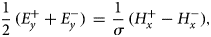
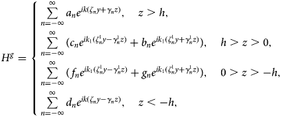
We consider scattering of the H-polarized wave by periodic finite and SIS of identical layers with cross-section shown in Fig. 1. The period is L and the number of layers in finite system is M. Every layer is ISG of graphene strips with the width 2d, located in the middle of dielectric slab of the thickness 2h and relative permittivity ε. The period of ISG is l.
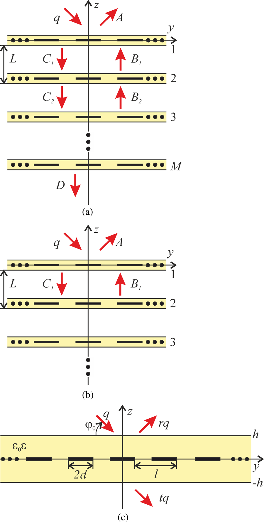
Fig. 1. The scattering geometry. (a) Finite system of layers, (b) SIS, and (c) single layer forming the multilayer structure.
At first, we consider single layer. After obtaining reflection and transmission matrices of a single layer we will use in the equations for the finite system and SIS.
Single layer
Let us consider the planar ISG of graphene strips embedded into a dielectric slab (see Fig. 1(c)). In [Reference Zinenko, Matsushima and Nosich18], a similar problem was considered with the use of the MAR. Here, in this paper, we will present SIE of the same form as in the case of finite grating. This will allow us to use the unified algorithm of solution as in the case of finite gratings as well as in the case of ISG.
We seek total electromagnetic field in the form H x = H i + H s + H g, where H i is the incident field, H s is the field scattered by the isolated dielectric slab (without graphene strips), and H g is the field scattered by the graphene strips. Usually H i + H s is called the primary field [Reference Zinenko, Matsushima and Nosich18]. It can be found analytically by enforcement of boundary conditions at the vacuum–dielectric interfaces.
As one can know, the field scattered by ISG can be represented as Fourier series. The considered scattering geometry consists of several domains: z > h, − h < z < h, z < − h. In every domain, H g can be represented as Fourier series with amplitudes that are unknown:
 $$H_{}^g = \left\{ \matrix{\sum\limits_{n = -\infty}^\infty {a_ne^{ik(\zeta_ny + \gamma_nz)}}, \quad z \gt h, \hfill \cr \sum\limits_{n = -\infty}^\infty {\lpar {c_ne^{ik_1(\zeta_n^1 y-\gamma_n^1 z)} + b_ne^{ik_1(\zeta_n^1 y + \gamma_n^1 z)}} \rpar }, \quad h \gt z \gt 0, \hfill \cr \sum\limits_{n = -\infty}^\infty {\lpar {\,f_ne^{ik_1(\zeta_n^1 y-\gamma_n^1 z)} + g_ne^{ik_1(\zeta_n^1 y + \gamma_n^1 z)}} \rpar }, \quad 0 \gt z \gt -h, \hfill \cr \sum\limits_{n = -\infty}^\infty {d_ne^{ik(\zeta_ny-\gamma_nz)}}, \quad z \lt -h, \hfill} \right.$$
where k = 2π/λ is the wavenumber in vacuum,  $k_1 = \sqrt \varepsilon k$, ζ n = 2πn/(kl) + cosϕ 0,
  $\gamma _n = \sqrt {1-{\lpar {\zeta_n} \rpar }^2}$,
  $\zeta _n^1 = 2\pi n/(k_1l) + \cos \phi _1$,
  $\gamma _n^1 = \sqrt {1-{\lpar {\zeta_n^1} \rpar }^2}$,
  $\cos \phi _1 = \cos \phi _0/\sqrt \varepsilon $, ϕ 0 is the incidence angle calculated from the negative direction of the y axis, and a n, c n, b n, f n, g n, and d n are amplitudes. Note that in (2) we take into account the radiation conditions analytically.
For determination of unknown amplitudes in (2) using boundary conditions (1) and conditions at the vacuum–dielectric interface, the following dual integral equations can be obtained, written for a single period |y| < l:
 $$\sum\limits_{n = -\infty} ^\infty {{\hat{b}}_ne^{ik_1\zeta _n^1 y}} = 0,\quad \vert y \vert \ge d\,,$$
 $$\displaystyle{{2ik_1\sqrt \varepsilon} \over {\sigma Z}}\sum\limits_{n = -\infty} ^\infty {{\hat{b}}_ne^{ik_1\zeta _n^1 y}} + ik_1\sum\limits_{n = -\infty} ^\infty {{\hat{b}}_n\gamma _n^1 \displaystyle{{1-C_n} \over {1-G_n}}e^{ik_1\zeta _n^1 y}} = -\displaystyle{\partial \over {\partial z}}H_{}^{slab}, \quad \vert y \vert \lt d\,,$$
where Z = 120π Ohm,  $\hat{b}_n = (b_n-g_n)$, C n = c n/b n, G n = g n/b n, and H slab = H i + H s. Expressions for c n and g n are known, they are too lengthy and are not given here. Amplitudes a n, f n, and d n also can be expressed in terms of b n.
As it is usually done for ISG, introduce dimensionless quantities ξ = 2πy/l, κ = k 1l/(2π), and δ = 2πd/l. Introduce the function
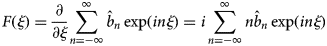 $$F(\xi ) = \displaystyle{\partial \over {\partial \xi}} \sum\limits_{n = -\infty} ^\infty {{\hat{b}}_n\exp (in\xi )} = i\sum\limits_{n = -\infty} ^\infty {n{\hat{b}}_n\exp (in\xi )} $$
From (3) we can find that F(ξ) = 0, when |ξ| > δ, hence
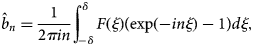 $$\hat{b}_n = \displaystyle{1 \over {2\pi in}}\int_{\!\!-\delta} ^\delta {F(\xi )\lpar {\exp (-in\xi )-1} \rpar d\xi},$$
Then, with the use of the periodic Hilbert transform [Reference Zygmund26] with the singular kernel, from (4) and (5) we obtain SIE with additional condition over the finite interval ( − δ, δ)
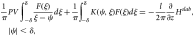 $$\displaystyle{1 \over \pi} PV\int_{-\delta} ^\delta {\displaystyle{{F(\xi )} \over {\xi -\psi}} d\xi} + \displaystyle{1 \over \pi} \int_{\!\!-\delta} ^\delta {K(\psi, \xi )F(\xi )d\xi} = -\displaystyle{l \over {2\pi}} \displaystyle{\partial \over {\partial z}}H^{slab},\quad \vert \psi \vert \lt \delta, $$
 $$\displaystyle{1 \over \pi} \int_{\!\!-\delta} ^\delta {F(\xi )d\xi} = 0\comma$$
where
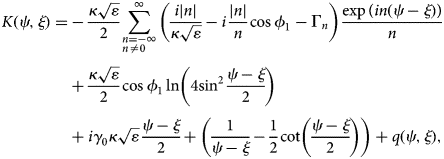 $$\eqalign{K(\psi, \xi ) = &-\displaystyle{{\kappa \sqrt \varepsilon} \over 2}\sum\limits_{\scriptstyle n = -\infty \hfill \atop \scriptstyle n\ne 0 \hfill} ^\infty {\left( {\displaystyle{{i \vert n \vert} \over {\kappa \sqrt \varepsilon}} -i\displaystyle{{ \vert n \vert} \over n}\cos \phi_1-\Gamma_n} \right)} \displaystyle{{\exp \lpar {in(\psi -\xi )} \rpar } \over n} \cr & + \displaystyle{{\kappa \sqrt \varepsilon} \over 2}\cos \phi _1\ln \left( {4{\sin}^2\displaystyle{{\psi -\xi} \over 2}} \right) \cr & + i\gamma _0\kappa \sqrt \varepsilon \displaystyle{{\psi -\xi} \over 2} + \left( {\displaystyle{1 \over {\psi -\xi}} -\displaystyle{1 \over 2}\cot \left( {\displaystyle{{\psi -\xi} \over 2}} \right)} \right) + q(\psi, \xi ),} $$
 $$q(\psi, \xi ) = \left\{ {\matrix{ {\displaystyle{{2i\kappa \pi \varepsilon} \over {\sigma Z}},} \hfill & {\xi \le \psi,} \hfill \cr {0,} \hfill & {\xi \gt \psi,} \hfill \cr}} \right.$$
 $$\Gamma _n = \gamma _n^1 \displaystyle{{1-C_n} \over {1-G_n}},$$
is the kernel function.
The Meixner's edge condition will be satisfied if unknown function F(ξ) has inverse square root singularities near the edges of the strip,  $F(\xi )\; {\sim}\; {1} / \sqrt {\delta ^2-\xi ^2} $, ξ → ±δ. To solve (7)–(9) we use the Nystrom-type method [Reference Gandel and Kononenko27, Reference Nosich, Gandel, Magath and Altintas28]. Taking into account the behavior of F(ξ) near the edges of the strips we chose the Gauss–Chebyshev quadrature with nodes taken at the zeros of the Chebyshev polynomials of the second kind.
Solution of (7) and (8) with the use of (6) allows us to obtain unknown amplitudes in (2). Suppose that the incident field is a set of plane waves with the vector of Fourier amplitudes q, reflected and transmitted fields are defined by the vectors a and d. Then, the reflection r and transmission t operators (matrices) of a single layer can be introduced as follows:
 $$a = rq,$$
 $$d = tq.$$
In the H polarization case,
 $$t = I-r,$$
where I is the unit matrix.
Finite system of layers
In [Reference Kaliberda, Lytvynenko and Pogarsky20], we used operator equations to determinate the spectral functions of the field scattered by the multilayer system of finite gratings. The same equations also can be written for multilayer system of ISGs:
 $$P = rq-reB_1 + eB_1,$$
 $$B_1 = q-rq + reC_1,$$
 $$C_1 = reB_1,$$
 $$B_m = eB_{m + 1}-reB_{m + 1} + reC_m,$$
 $$C_m = reB_m-reC_{m-1} + eC_{m-1},\quad m = 2,\,3,\,...\,,M-2,$$
 $$B_{M-1} = reC_{M-1},$$
 $$C_{M-1} = reB_{M-1}-reC_{M-2} + eC_{M-2},$$
 $$D = eC_{M-1}-reC_{M-1},$$
where P, D, B i, and C i are vectors of the Fourier amplitudes of the reflected, transmitted field and field between the layers. The directions of propagation of corresponding plane waves are shown in Fig. 1(a). Equations (13)–(20) are the matrix equations of the second kind. Taking into account diagonal matrix e with elements  $e^{ik\gamma _nL}$ that decay exponentially, when n → ∞, infinite matrixes in (13)–(20) can be truncated to the finite ones.
Semi-infinite system of layers
SIS is infinitely extended in one direction. It can be obtained from the finite structure by assuming M → +∞ and can be considered as a model of finite grating with extremely large number of layers. To build the mathematical model of SIS we use so-called translation symmetry that means that no SIS properties change with it first layer removed [Reference Lytvynenko and Prosvirnin29]. We denote as  $\Re $ the unknown reflection operator (matrix) of SIS. Than the vector of the Fourier amplitudes of the reflected field P can be obtained as
 $$P = \Re q.$$
At the same time, the reflected field can be represented as a superposition of two fields with amplitudes rq and teB 1:
 $$P = rq + teB_1.$$
Taking into account that the structure which consists of layers with numbers 2, 3, …, ∞ is also SIS, amplitudes B 1 and C 1 are connected as follows:
 $$B_1 = \Re eC_1,$$
 $$C_1 = tq + reB_1.$$
After transformations of (21)–(24), taking into account (12), one can obtain non-linear operator equation
 $$\Re = r + t\lpar {I-e\,\Re e\,r} \rpar ^{-1}e\,\Re \,e\,t.$$
Numerical results
Let us consider scattering of a normally incident plane wave with unit amplitude, ϕ 0 = 90°. To solve SIE with additional conditions (7) and (8) we used 100 nodes in quadrature rule in the Nystrom-type method, and we calculate the kernel function (9) with error less than 10−4. The transmission and reflection matrices of a single layer are calculated with four evanescent Floquet's modes taking into account. In the considered frequency range only dominant and ±1 Floquet's modes can propagate. Thus, the size of the transmission and reflection matrices, t and r, is 6 × 6. As numerical study of convergence shows it is enough to obtain accurate results. To solve (25) we used the successive over-relaxation method.
To validate our results we compare them with results obtained by MAR [Reference Zinenko, Matsushima and Nosich19] in the case of double-layer-graphene grating embedded into one dielectric slab, i.e. for 2h = L, M = 2. Chemical potential μ c = 0.39 eV, electron relaxation time τ = 1 ps, and room temperature T = 300 K. The dependence of the reflection coefficient is shown in Fig. 2, and good agreement is observed.
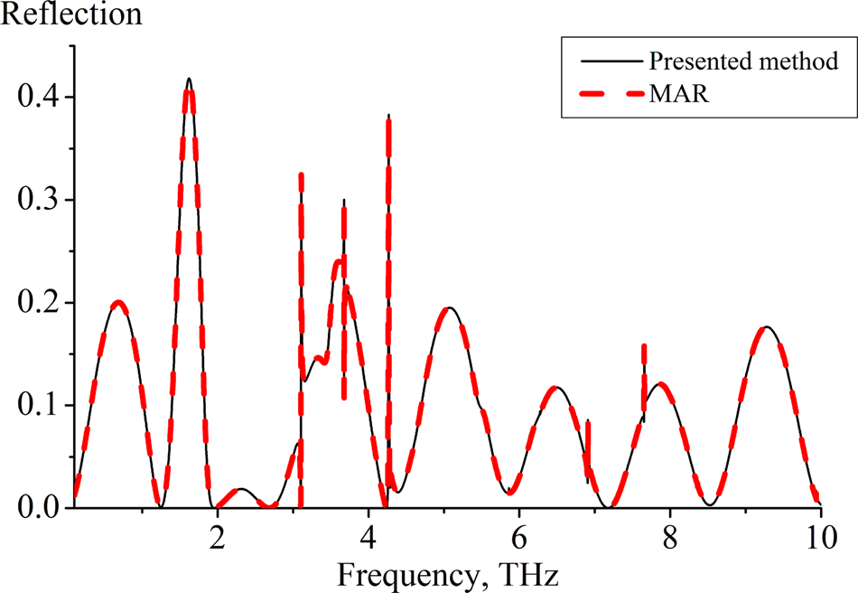
Fig. 2. Dependences of the reflection coefficient on the frequency for M = 2, d = 10 μm, l = 70 μm, L = 35 μm, 2h = L, μ c = 0.39 eV, τ = 1 ps, T = 300 K, ϕ 0 = 90°. Present method (solid line) and MAR (dashed line).
Figure 3 shows dependences of the reflection, transmission, and absorption coefficients (power) on the frequency for different number of layers and fixed value of chemical potential μ c = 0.39 eV. The dependences for finite structures approach to that of SIS with the number of layers are increased. The oscillations of the reflection and transmission coefficients of finite structures are observed at the opacity bands.

Fig. 3. Dependences of the (a) reflection, (b) transmission, and (c) absorption coefficients on the frequency for M = 2 (dashed line), M = 10 (solid line), and SIS (dotted line), d = 10 μm, l = 70 μm, L = 50 μm, h = 17.5 μm, μ c = 0.39 eV, τ = 1 ps, T = 300 K, ϕ 0 = 90°.
Figure 4 shows dependences of the reflection and absorption coefficients on the frequency for different values of chemical potential for SIS. The behavior of the curves in Figs 3 and 4 can be explained in terms of resonances that the structure under study can support.
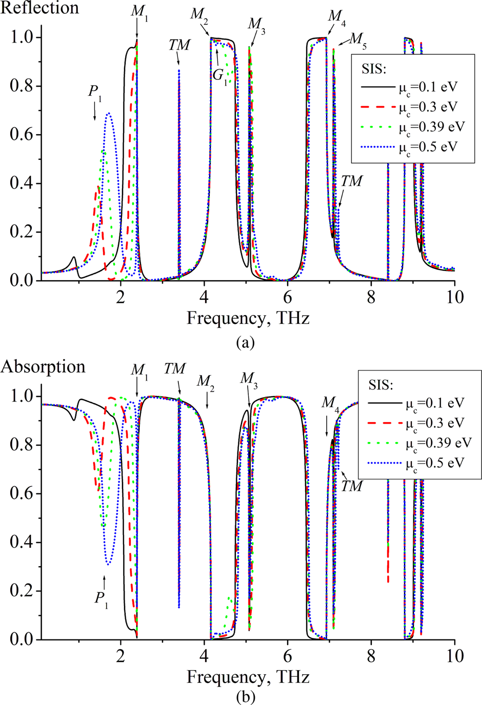
Fig. 4. Dependences of the (a) reflection and (b) absorption coefficients on the frequency for SIS, μ c = 0.1 eV (solid line), μ c = 0.3 eV (dashed line), μ c = 0.39 eV (dotted line), and μ c = 0.5 eV (short-dotted line), d = 10 μm, l = 70 μm, L = 50 μm, h = 17.5 μm, τ = 1 ps, T = 300 K, ϕ 0 = 90°.
Graphene strips can support plasmon resonances. They are marked as P i. In the case of normal incidence only odd-index resonances can arise. As one can see from Figs 3 and 4, variation of chemical potential results in a shift of plasmon resonances along the frequency axis. Their position can be controlled by electrostatic doping. The increment of the number of layers leads to grows of the absorption. The absorption coefficient of SIS almost equal 1, A → 1, near plasmon resonances.
In periodic strip grating embedded into a dielectric slab the grating-mode resonances can arise (marked as G i). Their nature is explained by the interaction of eigenmodes of dielectric slab with periodic structure. The dielectric slab acts here as a planar waveguide. The plane wave scattered by the strips excite the eigenwaves of this waveguide that propagate along the y axis. Further, eigenwaves interact with periodic system of strips, two adjacent strips act as a resonator. Near these resonances the sharp spikes are observed in the frequency dependences of the reflection and absorption coefficients. The position of grating-mode resonances depends on the parameters of dielectric slab and period of the grating and is practically independent of the parameters of individual graphene strip.
As is known, in the scattering of waves from finite multilayer structures, the stopband and passband effects appear. They are usually related to the phenomena of the propagating and non-propagating eigenwaves of similar however infinite-layer periodic media. On finite-layered structures, provided that the frequency is not in the stopband, such eigenwaves bounce between the first and the last layers that leads to the resonances (marked as M i in Figs 3 and 4). The propagation constant of the eigenwaves of the infinite multilayer medium can be found from the following equation [Reference Lytvynenko and Prosvirnin29]:
 $$\det \lpar {I-e^{-i\beta L}te-erer{(I-e^{i\beta L}et)}^{-1}} \rpar = 0.$$
Equation (26) can have several solutions. Under single mode approximation, i.e. dimension of all matrixes is 1, (26) has two independent sets of solutions. However, taking into account that the field is incident on the grating from z > 0 half space, only those solutions have sense that correspond to the eigenwaves propagating or decaying in the negative direction of the z axis.
Isolated dielectric slab can support slab-mode resonances (marked as S i). Their frequencies depend on the slab parameters and in our case are slightly perturbed by the graphene grating. The Q-factors of slab-mode resonances are low and they are overshadowed by the higher-Q plasmon resonance P 1 and the resonances of the multilayer grating M 2, M 4.
Finally, the family of resonances can be seen which we mark as TM. These resonances are also of the G-type, however they are the resonances on the other-type grating modes.
Figure 5 shows dependences of the reflection coefficient on the period L of the multilayer structure. The parameters of the structure are taken so that only one dominant plane wave can propagate between the layers. Dependences are almost periodic. The oscillations are observed at finite structures. The number of local maxima on the every period is equal to M − 1. As it is usual for multilayer systems, the stopbands and passbands appear. For the perfectly electric conducting strips, the stopbands correspond to values of the eigenwaves  ${\mathop{\rm Im}\nolimits} \beta \ne 0$. Since graphene strips absorb the electromagnetic field,
  ${\mathop{\rm Im}\nolimits} \beta \ne 0$ for all frequencies. The stopbands in Fig. 5 correspond to the maxima of
  ${\mathop{\rm Im}\nolimits} \beta $. Dependence of
  ${\mathop{\rm Im}\nolimits} (\beta )$ is shown in Fig. 6.
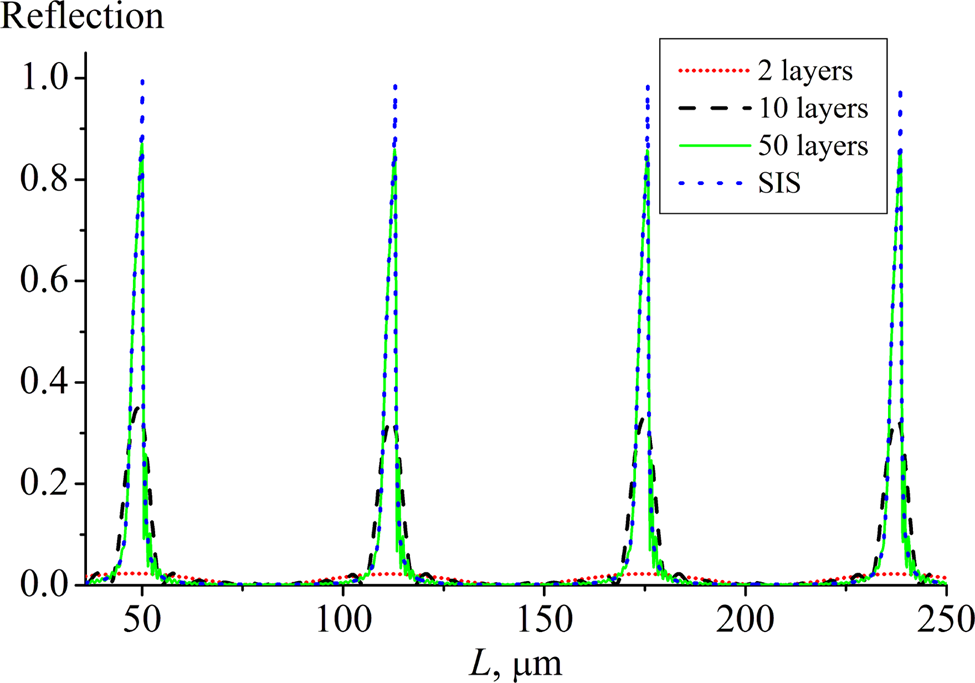
Fig. 5. Dependences of the reflection coefficient on the period of multilayer structure L for M = 2 (short-dotted line), M = 10 (dashed line), M = 50 (solid line), and SIS (dotted line), f = 2.3875 THz, d = 10 μm, l = 70 μm, h = 17.5 μm, μ c = 0.39 eV, τ = 1 ps, T = 300 K, ϕ 0 = 90°.

Fig. 6. Dependences of  ${\mathop{\rm Im}\nolimits} (\beta L)$ on the period of multilayer structure L. The parameters of the structure are the same as for Fig. 5.
Conclusion
We presented the rigorous method of analysis of scattering and absorption by multilayer-graphene system of ISGs embedded into the dielectric slab. Our approach allows reducing the dimension of the resulting matrix, since the whole considered structure is divided into several substructures.
We explain the behavior of the frequency dependences of the reflection, transmission, and absorption coefficients in terms of resonances that the structure under study can support. The resonances of the multilayer grating correspond to the maxima of imaginary part of the propogation constant of its eigenwaves.
We compared results for the finite and SISs. SIS represents more pronounced resonances that ease their identification.
The obtained results can find potential application in designing of frequency selective devices and absorbers. The presented algorithm can serve as a core in the design and optimization software of such devices.
Acknowledgement
This work was supported by the Ministry of Education and Science of Ukraine, grants 0118U002038 and 0117U004964.
 Mstislav E. Kaliberda received his B.S. and M.S. degrees in Applied Mathematics from V.N.Karazin Kharkiv National University, Kharkiv, Ukraine in 2005 and 2006, respectively, and his Ph.D. degree in 2013 from the same university. Now he is Associate Professor in the School of Radio Physics. His current research interests are analytical and numerical techniques, integral equations, multi-element periodic structures, and graphene gratings.
 Leonid M. Lytvynenko graduated from V.N.Karazin Kharkiv National University, Kharkiv, Ukraine and received combined B.S. and M.S. degrees in Radiophysics and Electronics in 1959 and his Ph.D. degree in 1965. From 1966 to 1985 he was with the Institute of Radiophysics and Electronics of the National Academy of Sciences of Ukraine (IRE NASU) in Kharkiv, Ukraine. He has been Professor in Radiophysics since 1977. In 1985, he founded the Institute of Radio Astronomy of NASU and served as its Director until 2017. His area of research is in the theory of wave scattering and propagation, antenna systems and engineering, microwave sources, and radio astronomy. He is vice-chairman of the Ukrainian National URSI Committee, member of the European Astronomy Society, and member of the International Astronomy Society. He is also the editor-in-chief of the journal “Radio Physics and Radio Astronomy.”
 Sergey A. Pogarsky received his M.S. degree in Radiophysics and Electronics from V.N.Karazin Kharkiv National University, Kharkiv, Ukraine in 1977, and his Ph.D. degree from the same university in 1984. Since 1977 he has been with the same university as researcher, and since 1984 as senior researcher and part-time senior lecturer at the Department of Physics of Ultra High Frequencies. Since 1999, he is Professor, and part-time Principal Scientist. His research interests include CAD techniques for microwave and millimeter wave components, antenna systems, and microwave transmission lines and circuits.


