


I. INTRODUCTION
Switch matrices have broad applications in redundant and broadcasting systems. Microwave and millimeter-wave switch matrices are essential components in telecommunication systems since they enhance satellite capacity by providing full and flexible interconnectivity between the received and transmitted signals. The demand for advanced switching systems has increased due to the recent growth in multimedia, mobile, and internet applications.
In satellite payload systems mechanical switches are still used, they exhibit low loss, but are bulky. Micro-electro-mechanical system (MEMS) technology has attracted tremendous interest across the world, and research efforts are constantly growing for reliability and integration purposes. MEMS fabrication techniques take advantage from the maturity of the fabrication technology commonly utilized in the production of integrated circuits (ICs). Several advances have been recently performed in the realization of radio frequency (RF) MEMS. The integration of MEMS into traditional RF circuits resulted in systems with superior performances and lower manufacturing costs. The incorporation of MEMS-based fabrication technologies into microwave and millimeter-wave systems offers viable routes toward ICs with MEMS actuators, antennas, switches, and transmission lines [Reference Kang, Kim and Chun1–Reference Di Nardo7]. The resulting devices operate with an increased bandwidth and with an increased radiation efficiency, and they are very promising for the implementation of aerospace and defense systems. A key role is played by the RF MEMS switches. These devices are able to process RF signals via a transmission line changing the state from on to off by means of an electrostatic actuation (but it can also be magnetic, piezoelectric, thermal, and so on) due to a voltage applied between a suspended metal membrane and an electrode. They pass from an up state to a down state generating an open or a short circuit on the TX line [Reference Yao and Chang8–Reference Rebeiz11]. This paper presents the tests performed on single-pole single-throw (SPST) ohmic series switches to be implemented in different topologies of single-pole 4-throw (SP4 T), double-pole double-throw (DPDT), and then integrated in LTCC technology for the realization of large-order Clos 3D networks. Two different SPST switches have been tested, based on cantilevers and clamped–clamped beams, both in coplanar waveguide (CPW) technology. The characterization was performed to select the best SPST configuration in terms of the RF and mechanical response of the switch. Specifically, the recorded data have been vital for simulations on a 16 × 16 matrix, in order to decide the matrix topology and the expected fulfillment of the electrical performances for the overall system. From preliminary simulations on such a system, based on single switch data coming from previous technological runs, large-order Clos 3D networks embedded in a LTCC structure would be the best candidates for the final matrix. The aim of this paper is to present the current state-of-art for an on-going European Space Agency (ESA) supported project. For this reason, we are presenting not only the building blocks characterization (single switches, SP4 T, and DPDT) but also the general aims for this activity, including the matrix simulations, because this will be the final output for the contract. In this way, the reader can have a better feeling of the full story, of the general requirements, and the currently available results. We have performed a comparison between two possible building blocks looking mainly to their electrical performances, leaving as a second future step the improvement in the reliability by using billion cycles, which is, by the way, not a critical issue for this application. For this reason, the single switches have not been stressed so much, because the main aspect is to evaluate highly reliable switches with a limited number of actuations. Specifically, the ESA program supporting this activity requires a maximum number of actuations for re-configuration purposes in the order of 1000.
II. DESIGN AND TECHNOLOGY
RF MEMS switches are subjected to various failure mechanisms, eventually leading to stiction during several or long-term actuations [Reference Stark12]. Charging effects due to dielectric layers used in the actuation pads are presently one of the most limiting factors in the device reliability [Reference Marcelli13]. Further to the optimization of the dielectric properties of the deposited oxides, in recent years some mechanical solutions have been developed to overcome such a problem. A solution consists in the realization of dielectric-free pads in order to avoid the contact of the bridge with the actuation pad [Reference Blondy14]. In this section, and in the following ones, the terms “pillars,” “stoppers,” and “stopping pillars” are used as synonyms. This non-contact configuration is possible by either realizing mechanical stoppers on the bottom surface of the bridge layer or building stopping pillars on the actuation pad. The latter solution has been adopted because it does not require any modification of the MEMS process previously developed for double-clamped beams within the consortium, and it is shown in Figs 1 and 2 [Reference Di Nardo7].

Fig. 1. Multi-layer technology to realize: (a) the contact bumps, (b) the stoppers, and (c) the electrodes for (d) the final device. LTO refers to low thermal oxide deposition by silane SiH4, TEOS to the higher temperature tetraethylorthosilicate deposition (Si(OC2H5)4). “Metal” means a multi-layer deposition comprising Ti/TiN/Al/Ti/TiN. The partial thicknesses used for the metal multilayer are, starting from the substrate toward the top surface are, in nm: Ti 30, TiN 50, Al 410, Ti 60, TiN 80 arriving to a metal having a total thickness of 630 nm, as it is shown in the figure. In particular, Ti 30 nm and TiN 50 nm are diffusion barriers toward the poly, whereas Ti 60 nm and TiN 80 nm on the surface are used for both diffusion barrier and to hindrance the hillocks formation during the LTO deposition.

Fig. 2. SEM picture of the double-clamped SPST series ohmic switch belonging to a SPDT structure. Two lateral wings are used for improving the electrical contact at the I/O ports. Details of the switch are given in the figure. “C” means the place where the metal beam is clamped.
All SPST switches are monolithically manufactured on p-type, 200 µm thick, highly resistive silicon wafers by using the eight-mask MEMS process developed at FBK-irst [Reference Di Nardo7]. The developed and tested series ohmic winged switches are summarized in Table 1, and the general structure is shown in Fig. 3. The dimensions of the bridge for this kind of switch are length = 500 µm and width (in winged area) = 150 µm. The cantilever switches are summarized in Table 2 and the structure is shown in Fig. 3. A high resistivity silicon substrate, with ρ > 5000 Ω cm has been used. The peculiar characteristics of the manufactured devices have been chosen to check the improvement due to the presence of both: (i) bumps under the wings, and (ii) pillars, for providing the full actuation but avoiding or minimizing the contact between the metal beam and the actuation pads. The first solution is used to improve the ohmic resistance of the actuated switch, because of the increasing number of contact points of the metal beam onto the substrate, balancing possible shape irregularities at the end of the beam (cantilever) or on the wings (double clamped structure). The second solution, already studied by other groups, provides an almost contact-less actuation, thus preventing or decreasing the charging effects. The manufacturing process includes a shaping along the double-clamped configuration, and selective gold electroplating. Au is thicker in the center with respect to the sides, to obtain a quite robust structure in the middle, but maintaining a good flexibility on the lateral sides (close to the actuation pads), thus facilitating the full collapse and a good electrical contact. The same conditions have been utilized for the cantilever, to obtain a robust, but easy to be actuated single-clamped configuration. The pillars, as it will be presented in the measurement section, are a valid technological solution to almost suppress the charging onto the actuation pads. On the other hand, some criticalities have still to be solved, because of the consumption of the pillars after a number of actuations, which can cause a premature failure of the switch when minded for billion of cycles. Technology is in progress to improve this manufacturing detail.

Fig. 3. Series ohmic winged switch. Lateral wings have been included for improving the electrical contact. When the switch is actuated, the bridge, isolated with respect to the ground, closes the central conductor of the CPW with a metal-to-metal contact and the device is in the ON state.
Table 1. Series ohmic winged switches description.

Table 2. Cantilever description.

The exploited configurations differ between them for the number of pillars, eventually using one stopping stripe only, and for the number of bumps (from 3 to 11), as expressed in Tables 1 and 2. Additional splits for the same basic configurations are the length of the wings, and the presence or absence of dielectric films onto the actuation pads. Square or circular bumps do not make an evidence for a shape dependence of the electrical response. Polysilicon has been used for the feeding lines, whereas TetraEthyl OrthoSilicate (TEOS) or Law Temperature Oxide (LTO) films have been deposited for the dielectric actuation pads (Fig. 4).

Fig. 4. Top view of the cantilever MEMS switch.
III. TEST PROCEDURES
The SPST devices have been tested by DC and RF measurements, with the goal to select the most promising configuration. In particular, five samples belonging to the same wafer, randomly chosen, have been characterized. It has to be stressed that, because of the peculiar application, i.e. signal routing for reconfiguration of the satellite, no failure is allowed for the SPST used as building blocks, or at least the limiting factors for their utilization have to be properly addressed. In particular, because the technology for implementing the presented configurations is still in progress for optimizing their electrical performances, we stopped the measurements when a significant change in the S-parameter response was recorded. The accepted changes in the S-parameters response have been defined at the beginning of the activity, according to ESA requirements on the final matrix structure. Actually, −10 dB should be the maximum acceptable loss for the 16 × 16 matrix, and −15 dB the return loss. As it will be demonstrated in the last section of this paper, the expected performances for the building blocks are tight, and they have to be compliant with the entire matrix requirements. Then, the SPST has to be very performant too. For this reason, an ohmic series switch has been evaluated to be a good candidate if its loss is in the order of −0.3 ± 0.1 dB, with a return loss not exceeding −30 dB up to 20 GHz.
The procedures and the obtained results are summarized in the following sub-sections.
The tests have been done under nitrogen flux with a temperature ranging between 23 and 24°C and relative humidity (RH) ≤30%.
A) DC test
The contact resistance versus the voltage Ramp signal (1 V/s) has been measured by using the experimental setup diagrammed in Fig. 5. The contact resistance versus the voltage Ramp signal (1 V/s) has been evaluated. The typical behavior for SW and CW switches is shown, where the resistance change due to actuation and de-actuation is given. It is worth noting that, in the studied configurations, charging prevention is obtained by means of pillars, avoiding the contact onto the actuation pads. In fact, the measured actuation voltage V act has been found to range between ca. 40 and 50 V for both configurations also after 105 cycles, and with unchanged RF performances at least up to 104 cycles for the CW device.
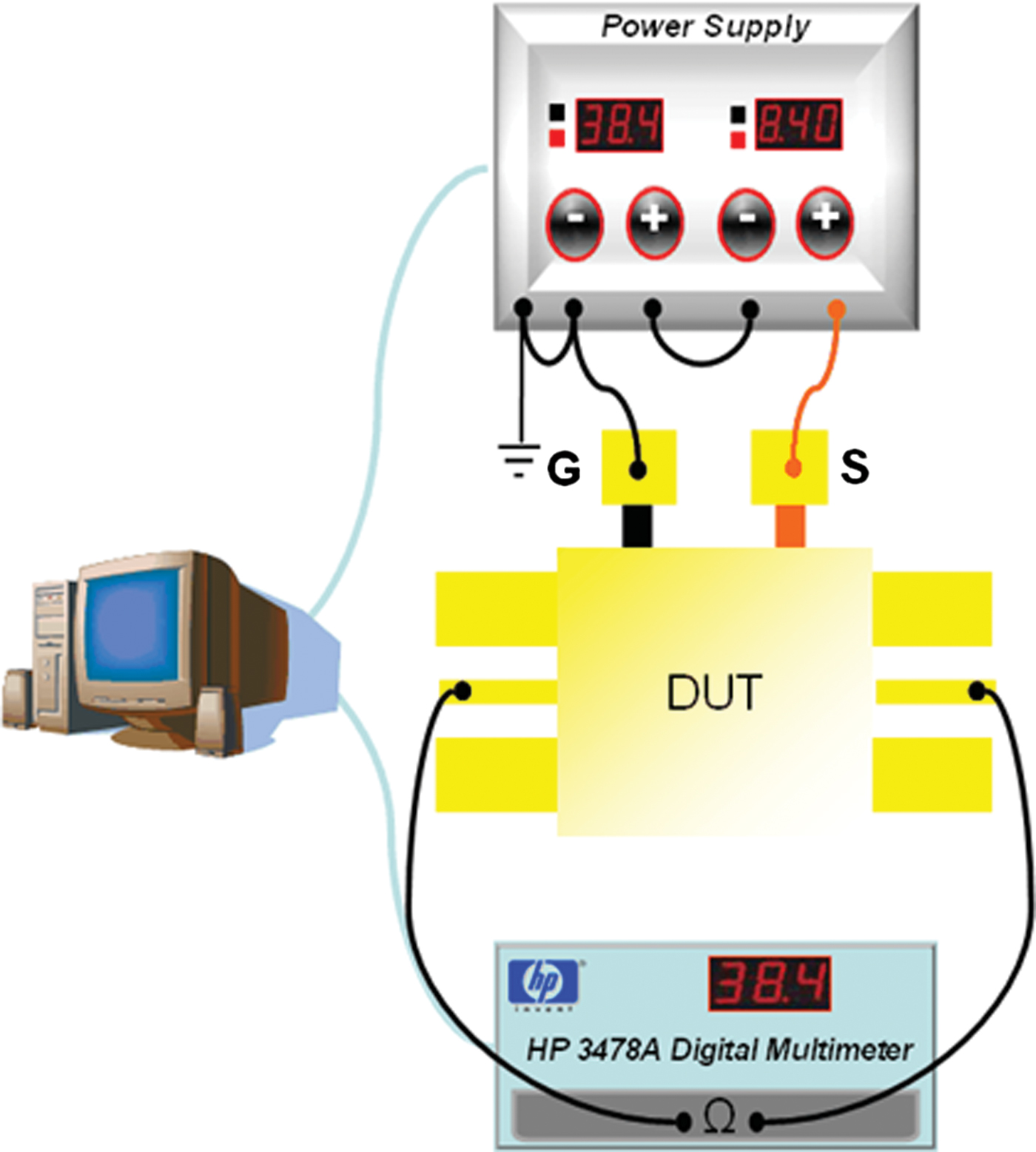
Fig. 5. Experimental setup for the characterization of the contact resistance of the ohmic switches. DUT is the device under test.
The typical behavior for the CW and SW switches is shown in Figs 6(a) and 6(b), where the resistance change due to actuation (voltage required to actuate the bridge) and de-actuation (voltage required to de-actuate the bridge) is given, together with a preliminary reliability test including cycles up to 105. In spite of a decrease in the performances due to the contact degradation because of the current flow, data belonging to the configuration labeled as CW are considered more promising for the future device implementations.
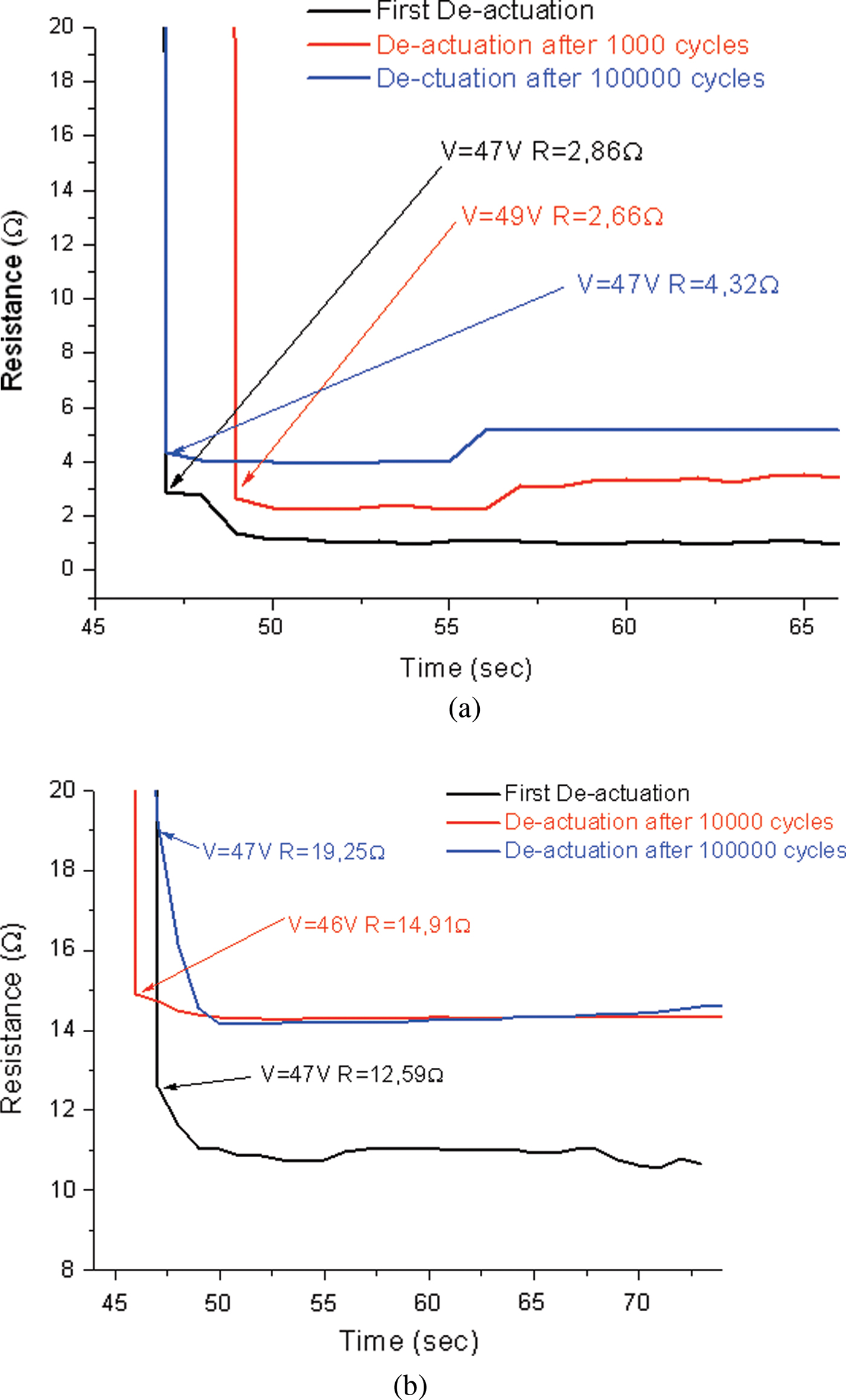
Fig. 6. Contact resistance of the CW (a) and SW (b) switches as a function of time. Reliability by means of cycles up to 105 actuations has been also measured. Better contact resistances have been measured for the CW configuration with respect to the SW one. De-actuation refers to the voltage at which the bridge is re-stored to the initial position, after being actuated.
Time offset is noticed in the pull-down response of the tested devices. It is not clear which is the cause for such an effect. The authors believe that the story of the device is affected by the number of cycles experienced, but no evidence, from the recorded data, is obtained on a reliable measurement of the offset.
1) RF test
On-wafer S-parameters of the switches, in the ON and OFF state, have been measured by means of a HP VNA 8510C from 45 MHz to 40 GHz, with commercial short-open-line-throw (SOLT) and in-house developed TRL calibrations. The experimental setup used for the RF characterization is shown in Fig. 7.

Fig. 7. The test bench is composed by the following instruments: one dual power supply for the devices actuation, one PC, one VNA, one waveform generator for the pulse train definition, two digital multimeters for controlling both actuation voltage and current flow (if any), one temperature-relative humidity sensor (T, RH% in the figure). The DUT is kept under nitrogen flow.
The environmental test conditions with for the measurement setup in Fig. 7 are: temperature T = 23°C and relative humidity RH ≈ 30%. For the RF test the following conditions have been imposed: SOLT calibration from 45 MHz to 40 GHz; power = 3 dBm, number of points = 801; multimeter resolution: current 1 µA, voltage 1 µV. A voltmeter (Hp3478 Digital Multimeter2) is in parallel between the actuation pads of the switch and the ground pad, to check the actuation voltage as close as possible to the device, and a current meter (Hp3478 Digital Multimeter1) is in line to check the amount of current flowing in the switch.
Scattering parameters have been recorded before and during the reliability test (up to 105 cycles) and the results are shown in Fig. 8 (isolation) and in Fig. 9 (return loss and transmission) for the SW switch in the OFF and ON configurations, respectively, whereas in Figs 10 and 11 the same findings are shown for the CW one. In Fig. 9 the insertion loss is more detailed with respect to the scale of the previous Fig. 8. In the captions of the following figures, an extended notation of the tested device has been used to indentify its position within the wafer. In particular, “L” and “C” mean “Line” and “Column” respectively, for a mask with several lines and columns containing repetitions of the same device structure.
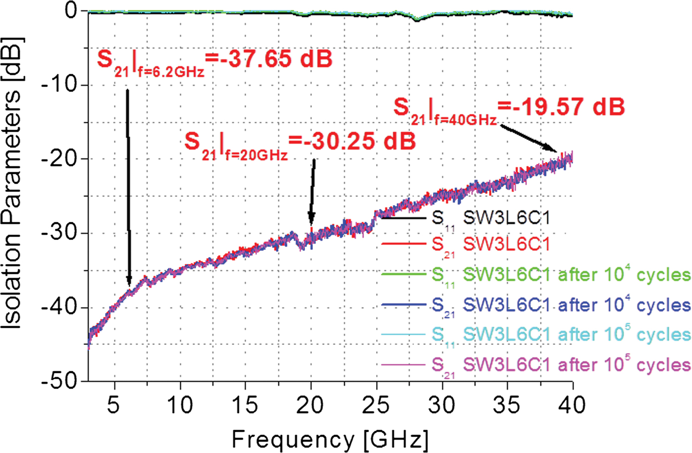
Fig. 8. Isolation performances of the SW switch. Curves are practically super-imposed.

Fig. 9. Return loss (a), and transmission (b) for the SW switch.

Fig. 10. Measured isolation performances for the CW switch up to 105 cycles.

Fig. 11. Insertion loss and return loss for the CW switch up to 105 cycles.
B) Environmental tests
1) Thermal tests
Thermal tests are important verifications for determining some of the reliability aspects in RF MEMS devices. Specifically, temperature can change metal shape and properties of the bridge, because stress can be induced in the clamped structure, with more evidence in a double-clamped one, where two mechanical constrains are present. Moderate thermal treatments contribute in the elongation of the metal, with significant variations of the actuation voltage because of the distance change between the metal beam and the wafer surface (gap). Such a voltage will decrease or increase depending on the direction of the residual stress characterizing the manufactured device. Higher temperatures can modify permanently the shape of the beam, and the metal will result in a damaged structure.
For testing the exploited devices, three kinds of experimental procedures have been followed:
(1) Gluing test: The switches have been glued on a gold plated Kovar carrier, using different temperatures: 30, 80, and 125°C.
(2) Thermal storage: The switches, glued at 30°C have been submitted to a thermal storage test, which has been performed with the following settings: 1000 h at 125°C in nitrogen ambient according to ESA PSS-01-612/Mil STD 883 – Method 1010, “B.”
(3) Thermal shocks/cycles: The switches subjected to the thermal storage test have been then measured under the following thermal shocks/cycles: 50 thermal shocks performed in nitrogen ambient, using a dual chamber, from −55 to +125°C (ESA PSS-01-612/Mil STD 883 – Method 1010, “B”). Ten thermal cycles performed again in nitrogen ambient, with T min = −35°C, and T max = +75°C. The temperature variation was imposed by means of a ramp R = 1 min/°C, with minimum and maximum temperature hold time of 1 h.
DC parameters (actuation voltage, contact resistance, de-actuation voltage) and RF parameters (S-parameters in up and down state) have been measured before and after all the thermal tests.
2) Vibration test (or mechanical test)
Vibration test is a standard characterization in space applications and, generally speaking, in harsh environments. For space, it means to check the response of the device or sub-system to be launched, for determining its sensitivity to specific steps of a mission, with special care for the launch of a satellite. Actually, the sizing of a spacecraft design is largely based on the launcher vibration loads. As everything that will go to space will have to be launched, vibration tests have to be scheduled when validating a technology for space. Moreover, during the launch phase the activity of the electronic and electromagnetic instruments on board is limited. Then, vibration environment of the launcher has to be taken into account together with the electromagnetic compatibility of every instrument belonging to the specific launcher. In our case, after the stress, the RF and any other designed specification have to be maintained.
The standard vibration test imposed for ground determination of the flight conditions during the launch consists of a sequence encompassing: Z-axis vibration, X-axis vibration, and Y-axis vibration. In turn, each axis vibration includes the following steps: the search for the resonance frequency, the sine vibration, and the random vibration, respectively. The DC parameters, including the following: (i) actuation voltage, (ii) contact resistance, and (iii) de-actuation voltage, and the RF parameters, including S-parameters in up and down state have been measured before and after the vibration test.
The results coming out from the above outlined thermal and mechanical tests are summarized in Tables 3 and 4.
Table 3. Actuation voltage for different SW switches measured on the same wafer after thermal and mechanical tests.

SW, SW2, etc. refer to devices taken from different positions within the wafer. Some failures have been recorded mainly for the SW configuration. The same happens for the CW devices. Structures manufactured on the edge of the wafer usually present higher actuation voltages, due to a thicker electroplated bridge. This effect appears to be less critical for the CW devices, mostly having V act in the order of 50–55 V.
Table 4. Scattering parameters of the SW and CW devices after temperature and mechanical stress.

F means failure.
From the analysis of the results presented in the previous tables it turns out that, presently, thermal cycling can be a killing factor for some of our devices. On the other hand, mechanical test performed on the same device after the thermal characterization is less critical and not dependent of the structure. Specifically, the cantilever configurations, having one constrain only from a mechanical stand point, are affected, as expected, by a change in the actuation voltage, but failure (F) after thermal cycle is less probable with respect to the double-clamped beams. Generally speaking, the SW devices (double-clamped) exhibit a trend in the decrease of the actuation voltage, probably due to a downward reshaping of the bridge up to possible sticking (micro-welding) for high temperatures, whereas the CW devices (cantilevers, single clamped) should exhibit an upward reshaping of the beam, with a resultant increase in the actuation voltage.
3) Endurance test
The endurance test has been performed with the aim to check the device response after voltage stresses, including cycling and continuous DC biasing.
It has been divided in two tests:
(1) Cycling stress test: Uni-polar biasing condition with a duty cycle of 50% and a frequency of 100 Hz has been applied to the device under test.
(2) DC stress test: A continuous uni-polar biasing signal has been applied for 10 min to the device under test. The S 21(V) test (S 21 parameters V s voltage from −100 to 100 V) has been used as parameter to check the performance of the SPST before, during, and after the tests as shown in Fig. 12. The amplitude of the signal voltage, used for the previous stress test, is adapted to the pull-in and pull-out voltage obtained in the S 21(V) test. It is usually set to 1.1–1.2 time the pull-in voltage.

Fig. 12. S 21(V) test for the CW switch at 8 GHz. The S 21 change due to the actuation of the SW switch before and after the DC stress is plotted, with full overlap between the initial and final curves. It is an evidence that the endurance test was passed without modifications in the electrical response of the device.
Looking at the results presented in the previous plots, the measured RF performances are in agreement with the expected ones, and with the required specifications for the building block of the matrix. For the series ohmic winged switches in the off state, isolation is well under −20 dB up to 30 GHz. Concerning the on state, a return loss better than −20 dB has been measured for all devices in the frequency band ranging from 45 MHz to 40 GHz. Insertion loss values vary a bit depending on the type of calibration, roughly ranging from −0.2 dB (TRL calibration) and −0.5 dB (SOLT calibration) for frequency values between DC and 20 GHz, giving evidence for an equivalent contact resistance of about 1.8 Ω.
All CW-type devices show an insertion loss better than −0.3 dB and return losses better than −30 dB from DC to 20 GHz. Isolation is better than −20 dB up to 13 GHz and better than −10 dB up to 40 GHz. All CW-type switches show on-state characteristics identical between them, as expected from simulations. Identical off-state isolation performances have been also measured, with the only exception of CW3 device, which shows an isolation which is about 2–3 dB better than the others. This is perfectly in agreement with what expected, since the switch has been designed with a reduced overlap area between the cantilever and the signal line. The CW-type switches are more robust than the SW-type switches, and they are characterized by a higher pull-in voltage. Owing to the results coming from the endurance tests, more attention will be focused on CW2 and CW4 test structures, which have exhibited the most promising results.
IV. SWITCH MATRIX DESIGN
With the proposed switches a 16 × 16 switch matrix will be built. From the simulations, a 3D Clos network embedded into an LTCC surrounding seems to be the best candidate. The general topology is depicted in Fig. 13. It consists of four stacked 4 × 4 blocks, repeated three times with a rotated orientation by 90°. The result is a very compact structure, each of the 12 blocks can easily be realized in LTCC. An extension to a bigger matrix can easily be done, just by stacking more sub-blocks with more in- and outputs. For example with 48 planar 16 × 16 sub-blocks a 256 × 256 matrix can be built by the same principle.

Fig. 13. 3D Clos configuration of the final matrix.
Clos networks are a subclass of the re-arrangeable networks [Reference Clos16]. Such a network consists of two symmetrical outside stages of rectangular sub-blocks with an inner stage of square sub-blocks. Here all sub-blocks are of 4 × 4 type. Each sub-block can be realized utilizing six DPDT switches in Beneš topology [Reference Beneš17] as shown in Fig. 13. An even more compact approach is based on SP4 T switches [Reference Casini15], where only eight SP4 T switches need to employed for one 4 × 4 sub-block.
The layouts of the SP4 T and DPDT based on the described ohmic switches in coplanar technology to be used in the switch matrix are shown in Fig. 14.

Fig. 14. (a) SP4 T switch based on SPDT switches with an additional shunt switch in the second stage, in order to improve isolation, and (b) DPDT switch based on ohmic switches.
The utilized SP4 T switch consists of a cascade of two SPDT switches realized with cantilever ohmic switches. In order to improve the isolation an additional shunt switch is added in every output path. The DPDT switch in Fig. 14(b) consists of four SPDTs, employing ohmic series switches of bridge type. The realization based on Beneš block with DPDTs exhibits more switches in one connection path; on the other hand, the connection circuitry is less complicated with a low number of crossings, which can be realized easily with only two layers of LTCC. The cross-section of on 4 × 4 block with the silicon chip embedded into a multilayer LTCC with metal package and connector pins is shown in Fig. 15.

Fig. 15. Cross-section of 4 × 4 sub-block.
To evaluate the RF transition performances, a full-wave simulation is performed part by part and their results are combined using circuit simulators for the feasible signal path [18, 19]. This is because the entire structure has lots of signal paths and their configuration is too complicated to perform a full-wave simulation. The simulation parts are carefully chosen so that the coupling with other parts is negligible for they cannot be taken into account during result combining by the circuit simulator. Every transition parts – layer to layer, bond wire, bond ribbon, RF pin connectors, etc. – are optimized to get feasibly best performances [Reference Kim, Faz and Vietzorreck20]. According to the simulation, the best results for the entire matrix were obtained by the 4 × 4 block utilizing SP4 T switches of which performances are depicted in Fig. 16.

Fig. 16. (a) Simulated return loss, (b) simulated insertion loss and (c) simulated isolation of the entire matrix based on 3D Clos network with SP4 Ts.
In the shown configuration a high isolation can be expected, as the coupling of signals in the SP4 T and especially between the isolated building blocks is low. The insertion loss is well above −10 dB up to 15 GHz due to the low number of employed switches in one pass. The only critical parameter is the return loss, which is comparably high because of the higher number of vias and connection pins. Here some more optimization of transitions and connections could lead to better results. With the Beneš network we obtained worse isolation, as more coupling within one DPDT occurs. The insertion loss is higher due to the higher number of employed switches. Only the return loss is comparable, here the connection circuitry is more simple; however, the number of transitions from the silicon blocks to the LTCC substrate is higher.
V. CONCLUSION
Cantilever and series ohmic winged switches for satellite applications have been fully tested. Cantilever switches exhibit better performances (lower contact resistance and insertion loss) with respect to clamped–clamped beam ones, and superior characteristics on all reliability aspects (including thermo-mechanical robustness). Moreover, they generally show a better agreement with respect to preliminary simulations and are less sensible to the stopping pillars manufacturing process. As a consequence, cantilever switches are currently preferred with respect to clamped–clamped beams. Dielectric layers on actuation pads prevent a reliable operation of the devices due to relevant charging effects, and this technological solution shall therefore be abandoned. The efficiency of the alternative solution, based on the utilization of stopping pillars, is confirmed by testing, and corrective actions in terms of geometry and dimensions shall be implemented on a second run in order to ease their manufacturing. Prototypes of SP4 T and DPDT with the switches shown in this paper have been already measured as reported in [Reference Casini15], and they will be implemented as soon as the corrective actions will be performed on the SPST devices. Matrix configurations using the proposed building blocks have been simulated for practical realization in an LTCC environment. Currently, sub-matrix elements have been manufactured with LTCC packaging. They are under test for final decisions about the assembly techniques to be followed for the full matrix, in order to fulfill the system requirements outlined at the beginning of Section III.
ACKNOWLEDGEMENTS
This work has been carried out in the frame of the ESA Project No. AO/1-5136/06/NL/GLC. The authors would like to thank Francois Deborgies from ESA/ESTEC for his support and suggestions.
 Giorgio De Angelis was born in Rome, Italy, in 1980. He received the Laurea degree in Electronic Engineering from the University of Rome “Tor Vergata,” Rome, in 2006, where he is currently working toward the Ph.D. degree in integrated circuits and telecommunications. He has been the recipient of a research fellowship on design, test, and reliability of frequency tunable RF microdevices at the Institute for Microelectronics and Microsystems, National Research Council (IMM-CNR), Rome, since 2006. His research interests include the design and test of microwave circuits and microelectromechanical systems devices for Space and Ground Applications.
 Andrea Lucibello was born in Rome, Italy, in 1980. He received the Laurea degree in Electronic Engineering at the University of Roma “Tor Vergata” in 2006. He is currently Ph.D. student at the same University and works since 2006 in collaboration with the CNR Institute for Microelectronics and Microsystems, involved in Technology and Test of RF MEMS for Space and Ground Applications.
 Emanuela Proietti received the degree in Electronic Engineering in 1996. Hired by the Texas Instruments Italia, Avezzano plant as Process Equipment Engineer in the CVD (Chemical Vapour Deposition) group as responsible of the oxide deposition. Participated in the technology transfer of Avezzano wafer fab from Texas Instruments production baseline of 0.21 µm to Micron Technology production baseline of 0.18 µm CMOS dynamic memory devices. In 1998, she became Lead Engineer of CVD group, responsible for whole CVD group processes and maintenances In 2000 hired by the ALCATEL Italia, Rieti plant as Maintenance Director for S.M.T. assembly production equipments. In 2001 she joined IMM-Rome as Research Engineer. From 2005 she is the Clean Room Area Responsible. She works in the high-frequency microsystems activity and she is involved in the experimental research of devices and microsystems.
 Romolo Marcelli was born in Roma, Italy, on February 26, 1958. He obtained the degree in Physics at the University of Roma “La Sapienza” in 1983. From 1987 he is with the National Research Council (CNR) of Italy, and from 1998 with the Institute for Microelectronics and Microsystems (IMM) of CNR. Presently, he is a Senior Researcher and responsible of the Research Line on High Frequency Microsystems: Technologies and Reliability for Ground and Space Applications at CNR-IMM Roma, where he is also responsible delegate of the IMM Director. His past and current interests include technologies, design, and test activities in microwave magnetics, RF MEMS, and metamaterials.
 Giancarlo Bartolucci graduated from the University of Roma La Sapienza in 1982 with a thesis on integrated optics. In 1982 he was with the “Fondazione Ugo Bordoni,” Roma. In 1983 he served as officer in the Technical Corps of the Army. From 1984 to 1992 he was a Researcher at the Department of Electronic Engineering of the University of Roma “Tor Vergata.”. Since 1992 he is an Associate Professor of microwave integrated circuits in the same Department. He was working on the development of equivalent circuits for microstrip and coplanar discontinuities. His current research interests are in the fields of the modeling of microwave and millimeter passive components, in particular for MEMS application, and in the study of new topology of phase shifters and filtering structures.
 Federico Casini was born in Perugia, Italy, on December 7, 1981. He received the Laurea degree in Electronic Engineering from the Università degli Studi di Perugia, Perugia, Italy in 2006. In 2006, he joined the Department of Electronic and Information Engineering (DIEI) of the University of Perugia (Italy) as a Ph.D. student, under the advice of Prof. Roberto Sorrentino. His research interest include design of RF beamforming networks; design of MEMS devices; design of dual-band antennas and antennas for WLAN applications. In February 2010 he received the Ph.D. degree from the University of Perugia, Italy.
 Paola Farinelli was born in Assisi, Italy, on September 19, 1978. She received the Laurea degree (with distinction) in electronic engineering from the University of Perugia, Italy, in 2002. In 2002 she joined the Department of Electronic and Information Engineering of the University of Perugia as a PhD student. In 2003 she conducted research work at the “Institut de Recherche en Communications Optiques at Microondes (IRCOM)”, Limoges University, (France). From November 2004 to May 2005 she has been a visiting researcher at VTT Millilab (Finland). In January 2006 she received the PhD degree and she is currently working at the University of Perugia as a contract researcher. Her research activity includes the electromagnetic modelling and design of reconfigurable RF MEMS devices such as SPnT switches, matrices, phase shifters, power dividers, filters.
Giovanni Mannocchi received the Degree in Electronic Engineering at the University of Perugia, Italy. He is currently Head of RF Products for Active Arrays and Project Manager at THALES ALENIA SPACE, involved in several activities for the qualification of Space Components and Sub-Systems, including RF MEMS applications. He is also Scientific Assistant at Technische Universität München.
Sergio Di Nardo. After his PhD in Physics, at the University of L'Aquila, he was research fellow for some years in the field of material physics. In 1998 he was recruited as Technology Engineer at Thales Alenia Space Italia (formerly Alenia Spazio).
Presently he is responsible of the Microelectronic Technologies – Techno Projects Unit at the Competence Center Electronics of Thales Alenia Space Italia.
He is responsible of the substrates technologies processes for microelectronic equipment (LTCC, Thick Film, Thin Film technologies). He is responsible of R&D activities on new materials and processes for substrates to be used in microelectronic equipment (LTCC, MCM-D poly based, MEMS, advanced packaging,…).
He participated to the definition and realization of several R&D projects in the field of microelectronic hardware for space applications (ESA, ASI, EU-FP7, …).
He was Technical Manager of several R&D projects.
His team supervises the technological aspects of the Thales Alenia Space Italia activities on RF-MEMS switches.
 Daniele Pochesci received the Degree in Electronic Engineering from the University of Roma “Tor Vergata”, Italy, in 2005. He was a Research Assistant at the Institute for Microelectronics and Microsystems (IMM) of the Italian National Research Council (CNR) in Roma from January 2006 to June 2007.
He joined Thales Alenia Space in June 2007 as microwave circuits designer and now he is involved in ESA research programs. Currently he is pursuing a PhD in Electronic Engineering at the University of Roma “Tor Vergata”.
 Benno Margesin received his doctor degree in Physics from the University of Bologna, Italy, in 1980. From 1982 to 1985 he was involved in the development of heavy ion sources and heavy ion implanters at the ITC-irst Material Science Division. In 1986 he joined the Integrated Circuit Laboratory at former ITC-irst where he worked on the development of low-temperature microcalorimeters and mixed ISFET/CMOS chemical sensors. Since 1997 he heads the Micromechanics Group of FBK-irst and since the beginning of 2008 he is responsible for the MEMS Research Unit of FBK. Currently, he is involved in the development of RF-MEM switches for space applications, microwave filters, capacitive microphones, and bolometer arrays.
 Flavio Giacomozzi graduated in Mechanical Engineering at the University of Padova in 1982. Since 1983 he is working at Fondazione Bruno Kessler, FBK (Former ITC- IRST), Trento Italy. From 1983 to 1988 he worked on the improvements of surfaces properties of materials. Since 1988, he has been with the Materials and Microsystems Division, where he was in charge of the development of fabrication processes technological steps. Since 1996 he is working on MEMS technologies and the realization of prototypes of several devices as sensors and microphones. Currently, he is involved mainly in the development and the fabrication of RF MEMS devices.
 Olivier Vendier earned his engineering degree in applied physics and a post graduate degree in microelectronics from the Institut National des Sciences Applique es in Toulouse in 1993. From 1993 to 1997 he worked as R&D engineer at the Georgia Institute of Technology, college of electrical engineering in Atlanta Ga, USA, where he got a Ph.D. degree in electrical engineering. Starting in summer 1997, he was part of the technical staff from the Technology Department at Thales Alenia Space where he was involved in various advanced packaging based projects. He is now in the microwave product line department (advanced microwave study group) at Thales Alenia Space where he is heading the MNT activities for new generation of microwave products for space satellites. He is now responsible for the technology support to the Solid State Power Amplifier product line. He is currently project leader of EC funded project and for several ESA and CNES funded project in advanced packaging. He is also expert for the European commission in the NOE TARGET from the EC, focusing on power amplifier technologies. Dr. Vendier has published over 50 technical papers in various journals and conferences and holds six patents on advanced packaging for microwave applications.
 Taeyoung Kim received the B.S. degree in Mechanical Engineering and Electronic & Electrical Engineering from Pohang University of Science and Technology (POSTECH), Pohang, Republic of Korea, in 2003 and the M.S. degree in high-frequency engineering from the Technische Universität München (TUM), Munich, Germany, in 2008. Currently, he works as Research Assistant at the Lehrstuhls für Hochfrequenztechnik, TUM. His current research interests include design of RF MEMS switching matrices for space applications and microwave applications on metamaterials.
 Larissa Vietzorreck was born in Düsseldorf, Germany. She received her master's degree in Electrical Engineering (Dipl.-Ing.) from the Ruhr-Universität Bochum, Germany, in 1992. From 1992 to 1997 she was a Research Assistant in the Department of Electrical Engineering of the Fern Universität in Hagen where she was working toward her doctoral degree. In 1998, she joined the Lehrstuhl für Hochfrequenztechnik at the Technische Universität München, Germany, as an Assistant Professor. In 1999 she was Conference Secretary of the European Microwave Conference in Munich. She acts as reviewer for several journals and conferences and has published more than 80 contributions in journals and conference proceedings. Her current research interests are design and simulation of microstructured components and development of numerical software tools.


