I. INTRODUCTION
Planar antennas are the newest generation of antennas, boasting such attractive features as low profile, light weight, low cost, and ease of integration into arrays. These features make them ideal components of modern communications systems [Reference Wong1]. Also, with the commercial success of wireless handheld devices comes the important role of good manufacturing techniques. This is not only important for reducing the cost of mass production, but also for enhancing the design performance and size in a controlled fashion [Reference Anguera, Andújar, Huynh, Orlenius, Picher and Puente2].
Ultra-wideband (UWB) technology has received an impetus and attracted academia and industrial attention in the wireless world ever since Federal Communications Commission (FCC) released a 10-dB bandwidth of 7.5 GHz (from 3.1 to 10.6 GHz) [Reference Mishra and Mukherjee3]. Commercial UWB systems require small low-cost antennas with omnidirectional radiation patterns and large bandwidth [Reference Schantz4, Reference Ojaroudi, Ghanbari, Ojaroudi and Ghobadi5]. Over the UWB working band, there are some other existing narrowband communication systems, such as 3.4–3.69 GHz band (IEEE 802.16) Worldwide Interoperability for Microwave Access (WiMAX) and 5.15–5.825 GHz band (IEEE 802.11a) Wireless Local Area Networks (WLAN), which may cause possible electromagnetic interference to the UWB applications [Reference Gao, Xiong, Dai, He and Zheng6]. To overcome this problem, it is desired to design UWB antennas with band rejection characteristic and reconfigurable capability. In order to create band rejection antennas, several techniques has been proposed recently such as embedding parasitic elements [Reference Nasrabadi and Rezaei7–Reference Eshtiaghi, Nourinia and Ghobadi11], C- and S-shaped slot [Reference Nasrabadi and Rezaei12–Reference Qu, Li and Xue14], square slot [Reference Badamchi, Valizade, Rezaei and Badamchi15], cutting V-shaped slot [Reference Kim and Kwon16], and combining with the notched meta-material UWB filter [Reference Kahng, Shin, Jang, Anguera, Ju and Choi17].
Recently, we are seeing lots of great trends toward design and implementation of a reconfigurable defected ground structure (DGS), which is realized by etching a certain defected pattern or slot in the ground plane. The reconfigurable DGS can be used in many applications such as antennas due to their interesting properties in terms of size miniaturization, arbitrary stop-bands, and suppression of surface waves [Reference Fakharian, Rezaei and Orouji18–Reference Safarpour, Rezaei and Zarkhoshk21].
This paper presented a new microstrip slot antenna with switching capability for UWB applications. The designed antenna has the ability of operating in four different states. To achieve the performance of reconfiguring, two PIN diodes are used on the patch and ground plane. The needed modifications have been done on the square radiating patch and ground plane in order to achieve the UWB characteristics. The band-notched characteristics are mainly due to the change in surface current, which is determined by PIN diodes [Reference Borhani Kakhki, Rezaei and Valizade22]. The following sections deal with the antenna geometry, design procedures, simulation, and experimental results.
II. ANTENNA DESIGN AND CONFIGURATION
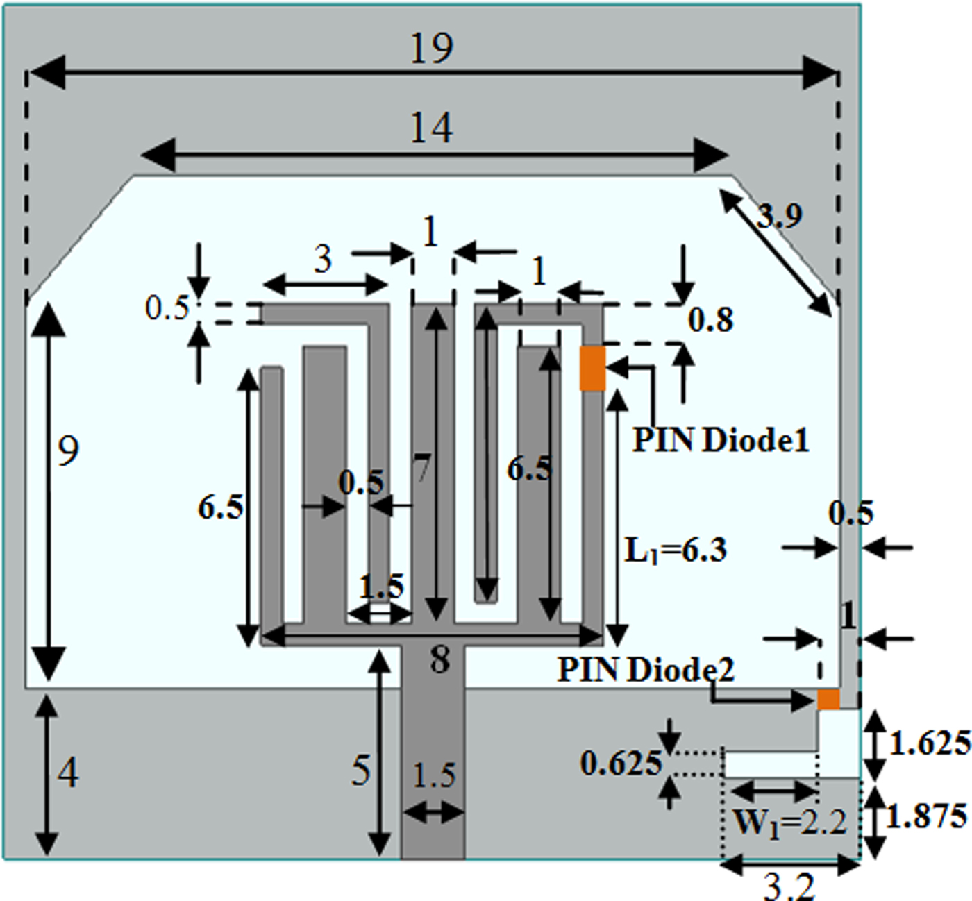
The proposed antenna structure with designed parameters is shown in Fig. 1.

Fig. 1. Geometry of the proposed microstrip slot antenna (unit, mm).
The antenna is printed on both sides of a low-cost FR-4 substrate with thickness of 0.8 mm, relative permittivity of 4.4, and loss tangent of 0.018. The antenna structure consists of a modified square-shaped radiating patch, a ground plane with L-shaped slot and feed line by size of 8 × 1.5 mm2. For signal transmission a SMA connector (SubMiniature version A) is connected to the feed-line. To achieve the performance of frequency reconfigurable, two PIN diodes are used on the antenna structure, which are placed in the antenna patch and ground plane. The proposed antenna is capable to switch among four different states.
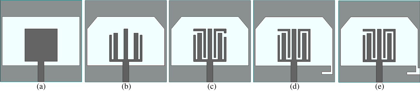
Figure 2 shows the various antenna structures in five steps, which are investigated during the simulation studies, and their return loss characteristics are compared in Fig. 3. To simulate the antenna and get return losses, Ansoft HFSS software is used [23].

Fig. 2. Simulated different antenna structures.

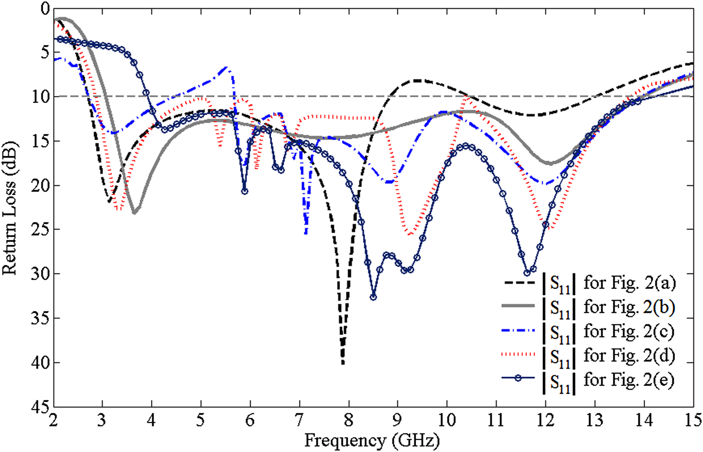
Fig. 3. Simulated return loss characteristics for the steps of antenna design.
Figure 2(a) shows an ordinary antenna, which consists of a square patch by dimension of 8 × 8 mm2 and a DGS, which provides a bandwidth of 2.7–8.8 GHz. According to Fig. 2(b), in order to improve the impedance bandwidth of 3 to over 13.6 GHz, square patch transformed to a fork-shaped patch and two triangular-shaped strips added at above sections of rectangular slot on the ground plane. The changes were obtained through simulation procedure and we realized that their dimensions play an important role in order to obtain desired result, whereas the absence of each slot on the patch or triangular-shaped strips at above sections of rectangular slot on the ground, eliminates the resulted bandwidth. As shown in Fig. 3, by adding two inverted L-shaped strips in the fork-shaped patch, band rejection from 4.51 to 5.7 GHz obtained (Fig. 2(c)). As can be seen in Fig. 3, adding an L-shaped slot to the ground plane and forming the antenna structure in Fig. 2(d), eliminates the created band rejection. By transforming of Figs 2(d)–2(e), the presented antenna satisfies the frequency range of 3.8–13.5 GHz, which is UWB performance with a band rejection in the WiMAX band.
In order to illustrate the operation theory behind the band rejection characteristics of the proposed antenna, the surface current distribution is depicted for three cases in Fig. 4. It can be seen from this figure that for different states of diodes, different part of the structure has a corresponding resonating path.

Fig. 4. Simulated surface current distributions on the proposed antenna: (a) antenna in UWB mode and (b) band-notch antenna with PIN diode 1 at 3.5 GHz. (c) Band-notch antenna with PIN diode 2 at 5.5 GHz.
To model PIN diode switch in the simulation, there are two techniques. In first technique, ideal switch models are used. This means that closed (ON) and opened (OFF) states of the switch are simulated in the presence or absence of a metal pad, respectively. In second technique, PIN diode is modeled as a capacitance/resistor in the OFF/ON state, respectively [Reference Borhani Kakhki, Rezaei, Sharbati and Fakharian24].
Figure 5 shows the equivalent circuits of the PIN diode. PIN diodes act as a variable resistance in radio frequency (RF) frequency. But in ON and OFF states, their circuit models are complicating. In both ON and OFF states, PIN diodes have an inductance in their structures. As can be seen in Fig. 5(a), when PIN diode is biased forwardly (ON state), the equivalent circuit of the diode consists of a small resistance and an inductance, which are series with each other. In the OFF state, when the diode is reversing biased, the equivalent circuit of the diode is composed of parallel combination of resistor and capacitor, which are series with an inductance [Reference Nasrabadi and Rezaei7].
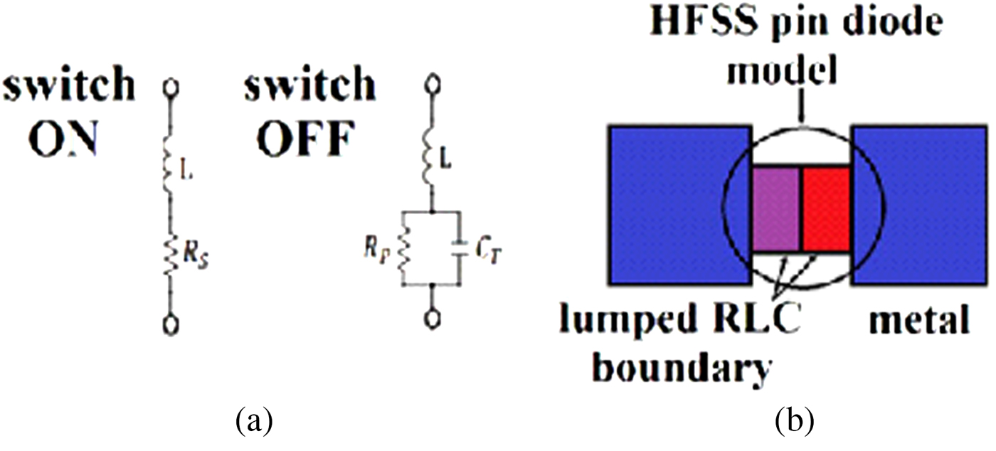
Fig. 5. RF PIN diode: (a) equivalent circuit model and (b) HFSS model.
In the designed antenna, to model PIN diode switches, both the mentioned techniques have been applied and we saw good agreement between their results.
III. PARAMETRIC STUDY OF THE PROPOSED ANTENNA
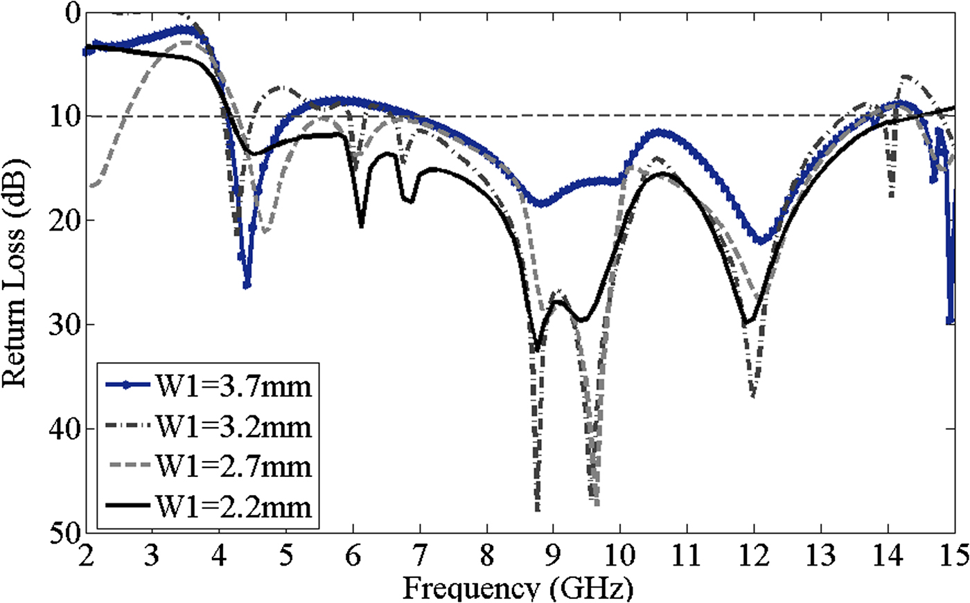
Parametric study is performed to obtain the final design values and optimize the performance of the antenna. Essential parameter in order to cause a band notch at WiMAX of the proposed structure is W 1. Figure 6 shows the simulated results of the proposed antenna with the effects of W 1 on adjusting band-notch performance in WiMAX. The results indicate that with decrease of W 1 from 3.7 to 2.2 mm, the notched frequencies can cover the WiMAX band, but there is undesirable notched frequency between 4 and 14.5 GHz when W 1 decreases from 3.7 to 2.7 mm with the step of 0.5 mm. However, for W 1 as 2.2 mm there is no undesirable notched frequency in mentioned range. Hence, the value of W 1 is optimized as 2.2 mm.

Fig. 6. Simulated return loss characteristics of the single-band-notch (WiMAX) antenna with different values of W 1.
IV. RESULT AND DISCUSSION
The photograph of the manufactured antenna is presented in Fig. 7. Simulated and measured return loss characteristics of presented antenna in four states are plotted and compared in Figs 8–11.

Fig. 7. Photograph of the slot reconfigurable antenna with bias circuit: (a) top view and (b) bottom view.

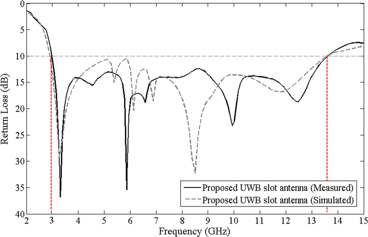
Fig. 8. Measured and simulated return-loss results in UWB antenna.
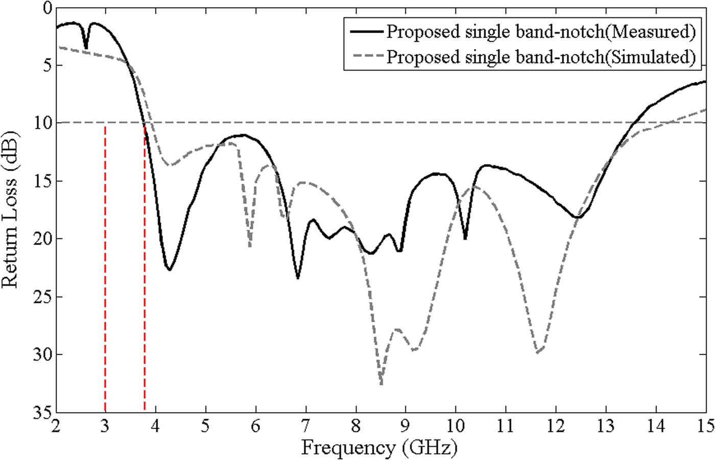
Fig. 9. Measured and simulated return-loss results in single-band-notch (WiMAX) antenna.
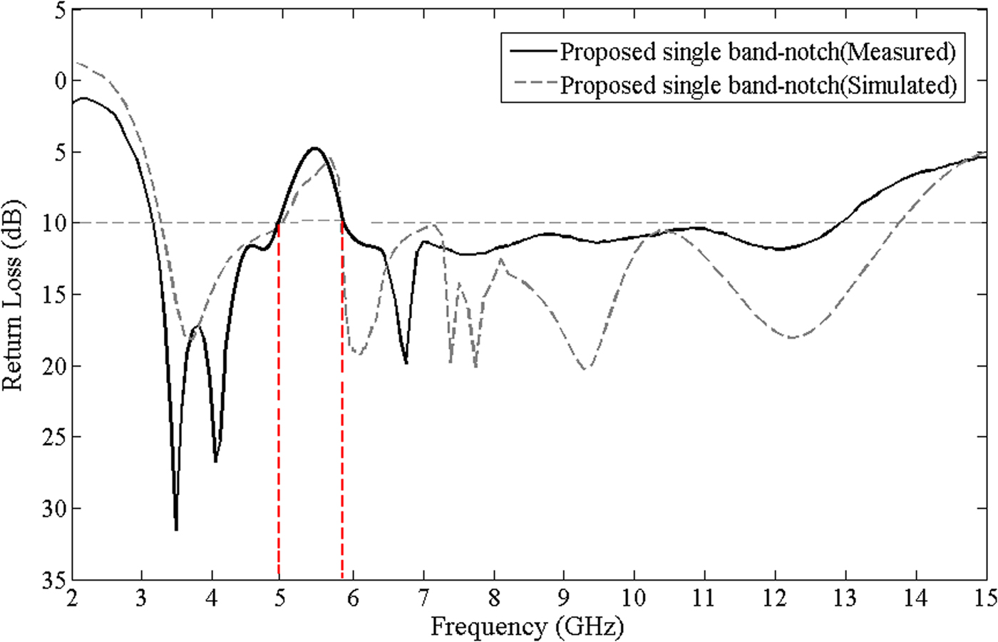
Fig. 10. Measured and simulated return-loss results in single-band-notch (WLAN) antenna.

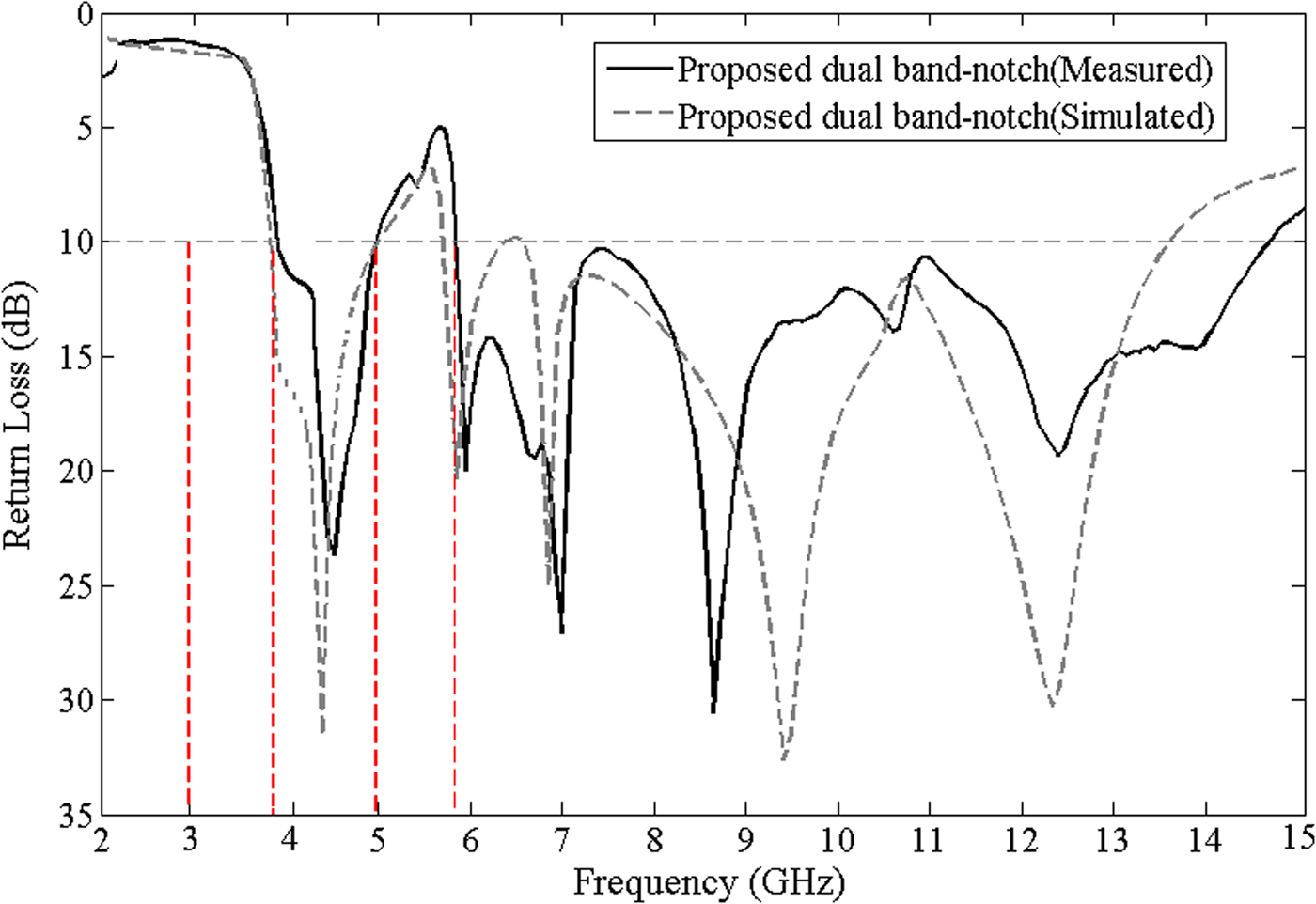
Fig. 11. Measured and simulated return-loss results in dual-band-notch (WiMAX and WLAN) antenna.
As can be seen in Fig. 8, the proposed antenna allows the frequency reconfigurability by activating two PIN diodes. When both diodes are ON, the presented antenna covers all the 3–13.5 GHz.
When D1 is ON and D2 is OFF, it is observed that the fabricated antenna satisfies the frequency range of 3.8–13.5 GHz, which is UWB performance with a band rejection in WiMAX (Fig. 9).
As shown in Fig. 10, by tuning diode 2 to ON and diode 1 to OFF, the band rejection of WLAN at 5–5.7 GHz is observed.
Finally and in the fourth state, by switching both PIN diodes OFF, dual-band rejection of WiMAX and WLAN at 3–4.2 and 5–5.78 GHz are achieved, respectively (Fig. 11).
As can be seen from the proposed results, there is good agreement between the measurement and simulation results, which confirms the accurate performance of the designed antenna. However, there is some discrepancy between the simulated results and measured data, which can be due to a number of reasons such as the implementation of the PIN diodes and their biasing circuits, the effects of the SMA connector and inaccuracies in the fabrication process [Reference Fakharian, Rezaei and Orouji25]. Schematic diagram and photograph of measurement setup of the antenna for the radiation pattern characteristics are shown in Fig. 12.
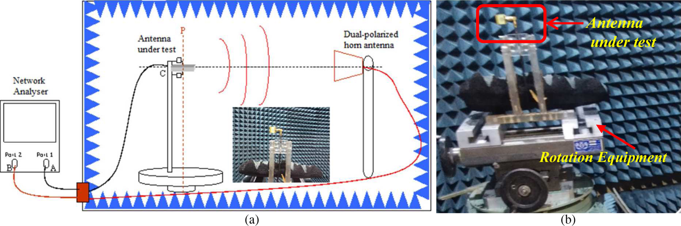
Fig. 12. (a) Schematic diagram and (b) photograph of measurement setup of the antenna for radiation patterns.
Figure 13 indicates the measured and simulated E- and H-plane radiation patterns for the manufactured antenna at three different spot frequencies 4.6, 7.5, and 10 GHz, respectively. As can be seen in Fig. 13, the H-plane pattern is nearly omnidirectional, which is desired for most related applications and the E-plane pattern depicts a dipole-like pattern in both measured and simulated results.

Fig. 13. Measured and simulated (H-plane) and (E-plane) radiation patterns of the antenna at: (a) 4.6, (b) 7.5, and (c) 10 GHz (not normalized).
At higher frequencies, the radiation pattern deteriorates because of unequal phase distribution and significant magnitude of higher order modes and also variation of the equivalent radiating area with frequency over UWB [Reference Wu, Jin, Geng and Ding26]. Omnidirectional characteristics and radiation bandwidth can be improved if the ground plane length is approximately the same size as that of the radiating structure width and also by using a thin substrate or a substrate with low dielectric constant [Reference Mishra and Mukherjee3, Reference Wu, Jin, Geng and Ding26].
Figure 14 shows that gain of the single- and dual-band-notch antennas from 2 to 14 GHz is between 0 and −6 dB.
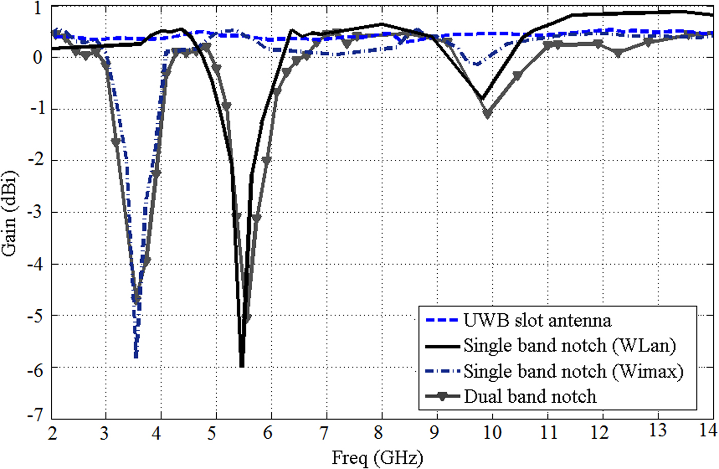
Fig. 14. Measured antenna gain of the proposed antenna.
In most passive circuits, dielectric constant and loss tangent of the FR-4 substrate increase as frequency increases. As a result, at the upper frequencies, it causes increasing in directivity and decreasing in gain. As can be seen in Fig. 14, there is a sharp decreasing trend in 10 GHz, which is due to the effects of the substrate losses with frequency.
V. CONCLUSION
In this paper, a new compact reconfigurable UWB slot antenna with four different switchable states has been presented. Band-notched functions are provided by etched slots on the patch and an L-shaped DGS. Simulation and measurement results show that the proposed antenna is able to cover the range of frequencies 3–13.5 GHz and a switchable frequency band rejection in the single- and dual-band WLAN and WiMAX. Frequency single- and dual-band-notched function is a solution to overcome the interference problem. The fabricated antenna has simple configuration and small size and it is suitable in a variety of wireless systems.
ACKNOWLEDGEMENTS
This work has been supported financially by Semnan University. The authors would like to thank all the members of Antenna Laboratory at Iran Telecommunication Research Center (ITRC), especially Mr. Solat, Mr. Akhlagh Pasand, and Mr. Mirabdollahi, for their cooperation. They would also like to thank Dr. Fakharian, Mr. Nasrabadi, and Journal reviewers for their valuable comments and suggestions, which helped to improve the quality of this paper.
 Mehri Borhani Kakhki received her B.S. degree in Electrical Engineering from Electrical and Computer Engineering Faculty of University of Sistan and Baluchesten, Zahedan, Iran, in 2013 and M.S. degree from Semnan University, Semnan, Iran, in 2015. Her research interests include reconfigurable microstrip antennas, meta-materials and EBG structures interaction with antennas, and RF passive components.
 Pejman Rezaei received his B.S. degree in Electrical Engineering from Communication Faculty, Tehran, Iran, in 2000, and M.S. and Ph.D. degrees from Tarbiat Modarres University, Tehran, Iran, in 2002 and 2007, respectively. Currently, he is an Associate Professor in Semnan University, Semnan, Iran. His current research interests are Electromagnetics theory, Antenna theory and design, Reconfigurable structures.