I. INTRODUCTION
Microstrip antennas are frequently used in many wireless communication systems because of their attractive features such as planer profile, low cost, light weight, and easy to fabricate [Reference Garg, Bhartia, Bahl and Ittipiboon1]. However, the types of applications of microstrip antenna are restricted by narrow bandwidth. Accordingly, increasing the bandwidth of microstrip antenna has been a primary goal of research in the field. In fact, many broadband microstrip antenna configurations have been reported in last few decades, such as increasing substrate thickness and decreasing its dielectric constant [Reference Schaubert, Pozar and Andrien2], using appropriate feeding technique and impedance matching method [Reference Pues and Van De Capelle3]. One of the popular methods to improve the bandwidth of a microstrip antenna is to create various resonant structures into one antenna by cutting slots of different shapes, such as U-shaped slot [Reference Weigand, Huff, Pan and Bernhard4], V-shape slot [Reference Deshmukh and Kumar5], and by adding more patches [Reference Targonski, Waterhouse and Pozar6]. These broadband methods cause some resonance frequencies to appear near the main patch and lead to the bandwidth broadening of the antenna. The capacitive coupled probe-fed microstrip antenna with wideband characteristics has been reported in [Reference Kasabegoudar and Vinoy7].
In the current wireless communication system, circular polarization (CP) is used as one of the most common polarization types, as it is independent of transmitter and receiver orientation [Reference Chang, Wong and Chion8]. The CP waves can be generated, when two orthogonal field components with equal amplitude but in phase quadrature are radiated. The CP antennas can be classified as single feed type or dual feed type depending on number of feed points [Reference Garg, Bhartia, Bahl and Ittipiboon1]. The dual feed approach requires the use of a 90° hybrid to provide necessary phase shift. However, this dual feed method has more complex geometry, larger size, and higher loss [Reference Garg, Bhartia, Bahl and Ittipiboon1]. Thus, preference is given to single feed circularly polarized microstrip antenna. A single feed circularly polarized operation of the square patch by truncating a pair of patch corners is widely used in the single patch [Reference Sharma and Gupta9]. Kin-Lu Wong and Jian-Yi Wu [Reference Wong and Wu10] have presented a design that involves cutting slits in the square patch to achieve CP. The CP of the square microstrip antenna with four slits and a pair of truncated corner is presented in [Reference Chen, Wu and Wong11]. The CP can also be achieved with a circular microstrip antenna by adding a tuning stub [Reference Wong and Lin12]. It has been shown in [Reference Iwasaki13] that CP can be generated by embedding a crossed shaped slot at the center of the circular patch. In [Reference Pozar and Duffy14], dual-band circularly polarized aperture-coupled stacked microstrip antenna is presented, but the design of the aperture-coupled stacked microstrip antenna is complicated because of its multilayer structure and feeding network. The CP in two distinct bands is realized by using two perpendicular ports and two power dividers to 90° phase shift for each band [Reference Yu, Yang and Elsherbeni15]. However, this structure cannot operate in both frequency bands simultaneously. The antenna presented in [Reference Fujimoto, Ayukawa, Iwanaga and Taguchi16] operates at dual frequencies with CP characteristics. The dual-band CP radiation is achieved by inserting slits and T-shaped elements at the patch. In [Reference Heidari, Heyrani and Nakhkash17], a single feed slotted patch structure is presented for generating CP in two frequency bands. This antenna has a problem that the axial ratio bandwidth is very narrow in both the frequency bands. Microstrip patch antenna with switchable polarization is presented in [Reference Chen and Row18, Reference Osman, Rahim, Gardener, Hamid, Mohd Yusoff and Mazid19] with the single feed. PIN diodes are used to obtain the polarization diversity characteristics of the antenna. Many studies have been reported in the literature that describes different methods for achieving the triple band CP operations [Reference Zhou, Chen and Volkis20–Reference Lio, Chu and Du23]. The stacked Microstrip patch antenna is used to achieve triple band CP radiation [Reference Zhou, Chen and Volkis20, Reference Doust, Clenet, Hemmati and Wight21]. However, dual orthogonal feed makes the antenna complex. In [Reference Falade, Rehman, Gao, Chen and Parini22], three layers stacked single feed microstrip antenna was designed to achieve triple band CP operation. A triple-band stacked design was introduced in [Reference Lio, Chu and Du23], but all these designs have a narrow axial ratio bandwidth in the three frequency bands.
In this communication, a capacitive fed microstrip antenna with reconfigurable CP is reported. The design of the antenna is carried out in three stages. In the first one, small isosceles right angle triangular sections are removed from diagonally opposite corners for the generation of CP. In the second stage, truncated patch was loaded with horizontal slits of unequal lengths to create dual CP bands and PIN diodes are inserted across the both slits to generate three circularly polarized bands. CP in three distinct bands is achieved by switching PIN diodes ON and OFF on the gap of horizontal slits. Finally, a wideband antenna with reconfigurable CP is designed. This employs an inclined slot embedded on the patch with PIN diode across the horizontal slits to achieve the broadband performance. The impedance bandwidth of proposed antenna is 66.61% (ON state) ranging from 4.42 to 8.80 GHz and 68.42% (OFF state) in the frequency range 4.12 to 8.91 GHz with axial ratio bandwidths of 4.42, 2.35, and 2.72%. The bandwidth of the presented antenna is increased from 51 to 66.61% (ON state) and 68.42% (OFF state) as compared to capacitive coupled probe fed microstrip antenna [Reference Kasabegoudar and Vinoy7] and also generates three distinct CP bands.
II. ANTENNA DESIGN
The geometry of reconfigurable circularly polarized capacitive coupled probe fed truncated corner microstrip antenna is shown in Fig. 1(a). A pair of opposite corner is truncated with equal side length of ΔL to excite two orthogonal modes with 90° phase shift that makes the antenna circularly polarized. A pair of horizontal slits of lengths L 1, L 2, and equal width w 1 with PIN diode is embedded on truncated patch to achieve three circularly polarized bands as shown in Fig. 1(b). In the simulation, ON condition of PIN diode is implemented with a through line of length 1 and width 0.5 mm. Figure 1(c) shows proposed antenna with reconfigurable CP. The slot is inclined at 135° with dimensions of 8 × 1 mm2.

Fig. 1. Geometry of capacitive coupled probe-fed microstrip antenna (a) with truncated corner, (b) with PIN diode and horizontal slits on truncated patch, (c) with PIN diode, horizontal slits, and inclined slot on truncated patch, (d) fabricated structure of the proposed antenna.
The radiating patch and feed strip are placed on an RO3003 substrate with thickness h = 1.56 mm, dielectric constant ε r = 3.0 and loss tangent = 0.0013 which rose in the air by g (6 mm). The SMA connector is used to connect the feed strip that capacitively couples the energy to the radiating patch. The separation between radiating patch and feed strip is d, feed strip length is t and width is s. The structure of the antenna is based on suspended capacitive fed microstrip antenna. The total height of the antenna (g + h) and effective dielectric constant are the key design parameters for the patch. The dimension of the radiating patch is calculated from the standard design expression after making necessary corrections in the key design parameter discussed above for the suspended dielectric [Reference Garg, Bhartia, Bahl and Ittipiboon1, Reference Kumar and Ray24]. The impedance bandwidth may be maximized by using the design expression [Reference Kasabegoudar and Vinoy7] given as
 $$g \cong 0.16\lambda _0 - h\sqrt {\varepsilon _r}, $$
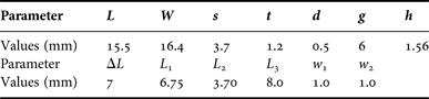
where g is the air gap, ε r and h are the dielectric constant and thickness of the substrate, respectively. Equation (1) is used to predict the initial value, while the final value would be within ±10% and may be obtained with simulation tools [Reference Kasabegoudar and Vinoy7]. The feed strip can be considered as a rectangular microstrip capacitor as strip dimensions are much smaller as compared to the wavelength of operation and can be represented by terminal capacitances. The dimensions (t and s) of the terminal capacitances control the reactive part of the input impedance of the antenna [Reference Kasabegoudar and Vinoy7]. The optimum dimensions of antenna obtained via iterative process that give broad impedance bandwidth and circularly polarized bands are listed in Table 1.
Table 1. Dimensions of antenna design.

The proposed antenna was fabricated in microwave research laboratory of Ambedakar Institute of Advanced Communication and Technologies Research (AIACTR), Delhi, India. The vector network analyzer of series Agilent N5230 was used for the measurement. The substrate of dimension 5 × 5 cm2 was taken for the fabrication and white paper board is used as support to provide an air gap.
III. RESULTS AND DISCUSSIONS
For the antenna design and simulation, IE3D simulation software is used which is based on MoM. The experimental verification is carried out to authenticate the antenna results. The final antenna is fabricated and is shown in Fig. 1(d) in ON and OFF states of the PIN diodes, respectively. The polarization of the antenna can be changed from linear to circular by truncating the opposite corners of the rectangular patch, which produces two orthogonal electric field components with equal amplitude and 90° phase difference. The single CP band with 3-dB axial ratio bandwidth of 11.1%, corresponding to the frequency range from 5.69 to 6.36 GHz is obtained with the truncation of dimension 7 × 7 mm2 at two opposite corners of the patch. Due to the truncation, the length of electrical patch decreases, which is responsible for gain reduction with respect to a reference antenna given in [Reference Kasabegoudar and Vinoy7]. PIN diode is used as a switch in several microstrip antennas. GaAs PIN diode with forward voltage 0.73 V and forward current 12 mA is used for switching the antenna. The inclusion of copper strip indicates the PIN diode in ON state, while the absence indicates the OFF state of the diode [Reference Osman, Rahim, Gardener, Hamid, Mohd Yusoff and Mazid19]. The equivalent circuit of the PIN diode for the ON state (forward bias), OFF state (reverse bias), and bias circuit to control the states of diodes are shown in Figs 2(a)–2(c), respectively [Reference Chen and Row18]. A thin slit in Fig. 1(c) is used for dc isolation and are connected to each other in an ac manner by capacitors. The aim here is to obtain the multiband CP operation. In order to achieve this aim, Fig. 1(a) is loaded with slits and PIN diodes. As a result, an antenna with triple CP bands is developed and the structure is shown in Fig. 1(b). Embedding slits with unequal length at the boundary of the truncated rectangular radiating patch and making the PIN diode ON and OFF is responsible for the multiband CP operation. Figure 3 shows the simulated reflection coefficient of the PIN-loaded antenna in OFF and ON condition of the diode. When the Diode is OFF, the antenna exhibits dual-band behavior in the frequency range from 4.39 to 6.42 GHz and from 6.98 to 8.27 GHz. The corresponding impedance bandwidth with OFF state of PIN diode is 37.55 and 16.97%. When the Diode is ON, the operating frequency is in the frequency range of 4.50 to 7.02 GHz and 8.4 to 8.87 GHz. The corresponding impedance bandwidth with ON state of PIN diode is 43.75 and 5.54%.

Fig. 2. Equivalent circuit and configuration of PIN diode bias circuit. (a) Forward bias, (b) reverse bias, and (c) bias circuit.

Fig. 3. Reflection coefficient of horizontal slit embedded truncated patch with PIN diode ON and OFF.
The variation of axial ratio with frequency is shown in Fig. 4 and it is observed that for three frequency intervals the axial ratio is below 3-dB, which indicates that the antenna can generate CP in three distinct bands. When the PIN diodes are OFF, it is like a simple notch in the antenna and splits the single-band CP into double CP band – one above and one below the original CP band. The two CP bands were obtained in the frequency range of 5.03–5.28 GHz and 6.61–6.80 GHz. The 3-dB AR bandwidth is 4.81 and 2.83%. It is seen that center frequency of CP operation is changed to 5.16 and 6.7 GHz from 6.025 GHz as in the antenna with truncated corners. The ON state of PIN diode is like an ohmic resistance and makes gap connected and electric currents flow through the path. This effect of changed electric length of the surface current changes the resonant frequency of the two near degenerate orthogonal modes and antenna gives CP at different frequencies. Figure 4 also shows the axial ratio of PIN diode loaded antenna with horizontal slits in the ON states of the diode. The 3-dB axial ratio bandwidth is 2.49% in the frequency range 4.75–4.87 GHz. It is seen from the figure that the antenna provides reconfigurable CP bands by tuning the PIN diodes.

Fig. 4. Axial ratio of horizontal slit embedded truncated patch with PIN diode ON and OFF.
Figure 5 shows the simulated gain of antenna under both conditions of the diodes. It is seen that gain drop in some frequency interval. The reduction of gain occurs in the frequency ranges, where radiation is not in-phase and the phase difference decides the gain. The reduced gain in the last CP band indicates higher order orthogonal modes combining to produce CP.

Fig. 5. Gain of PIN diode loaded truncated corner antenna with horizontal slits.
To increase the operational impedance bandwidth, an inclined slot was introduced in Fig 1(b) and proposed antenna is shown in Fig 1(c). The PIN diodes are intact at the gap between two edges of the horizontal slits. When an inclined slot is cut inside the patch, there is a further increase in the length of the surface current path along the patch. The inclined slot and PIN diode create two different resonances for the patch. The closeness among the resonances makes the broadband characteristic in the antenna. The broader bandwidth of the proposed antenna is due to the better control of current distributions towards the higher frequencies of the bandwidth that is achieved due to the inclined slot. Figure 6 shows the simulated and measured reflection coefficient of the proposed antenna with ON and OFF states of the PIN diode. The antenna shows an impedance bandwidth of 66.61%, ranging from 4.42 to 8.80 GHz with ON state of the PIN diode, while with OFF state of the PIN diode, the antenna operates in the frequency range of 4.12–8.91 GHz with an impedance bandwidth of 68.42%. In both states of the diode, the proposed structure provides better impedance bandwidth than previous work [Reference Kasabegoudar and Vinoy7]. The measured result shown for comparison is in good agreement with the simulated result. The mismatch between the measured and simulated results existed, which may be mainly caused by fabrication imperfection. Figure 7 shows the measured and simulated axial ratio of PIN diode loaded proposed antenna in the two states of the diode. It is clear from the figure that the antenna provides reconfigurable circularly polarized bands by tuning the PIN diodes. The antenna exhibits CP in two bands with the frequency range from 4.94 to 5.16 GHz and from 6.70 to 6.86 GHz, when PIN diode is OFF, i.e. axial ratio bandwidth is 4.42 and 2.35%, respectively. With ON state of the diode the antenna has another CP band from 4.71 to 4.84 GHz with axial ratio bandwidth of 2.72%. The 3-dB axial ratio frequency range for all the three CP bands falls within the impedance bandwidth. Figure 8 depicts measured and simulated gain with frequency for inclined slot loaded microstrip antenna with PIN diode ON and OFF. It is clear from the graph that the gain is almost constant over the CP bands. The gain of the antenna was measured in an anechoic chamber using the substitution method. Two calibrated horn antennas of known gain were used as transmit antenna to measure the gain of antenna under test (AUT). AUT was used as receive antenna and placed on the positioner with required elevation and azimuth coverage. The horn antenna with calibrated gain was used as source antenna. The similar measurement process was repeated by replacing AUT with another horn antenna of known gain. The difference between two measured powers reflects the gain difference and absolute gain of the AUT is calculated. By changing the distance between transmit and receive antenna, the process was repeated and the average gain was considered as the final gain.

Fig. 6. Measured and simulated reflection coefficient for the proposed antenna with pin diode ON and OFF.

Fig. 7. Measured and simulated axial ratio for proposed antenna with PIN diode ON and OFF.

Fig. 8. Measured and simulated gain for proposed antenna.
For the reception of the signal, it is important to find the direction of field rotation in terms of left hand circularly polarized (LHCP) wave and right hand polarized (RHCP) wave. The simulated and measured LHCP and RHCP far-field distribution in the E-plane at the center frequencies of individual CP bands 4.97, 4.77, and 6.78 GHz are shown in Figs 9(a)–9(c), respectively. From these figures, it is clear that the antenna is LHCP with considerable axial ratio beamwidth. A good amount of cross polar attenuation is obtained at all center frequencies.

Fig. 9. Simulated and measured LHCP and RHCP patterns at (a) 4.97 GHz, (b) 4.77 GHz, and (c) 6.78 GHz.
Figures 10(a) and 10(b) show the current distribution on the radiating patch for different time frames: t = 0(0°), t = T/4(90°), t = 2 T/4(180°), and t = 3 T/4(270°) at the center frequencies of CP bands with PIN diode OFF, while Fig. 11 shows the same at the center frequencies of the CP band with PIN diode ON. The surface current distribution of the radiating patch at the time frames clearly indicates the circularly polarized field radiation. The field rotates in the clockwise direction, which results in exciting a LHCP radiation.

Fig. 10. Surface current distribution for proposed antenna with PIN diode OFF at: (a) 4.97 GHz and (b) 6.78 GHz.

Fig. 11. Surface current distribution for proposed antenna with PIN diode ON at 4.77 GHz.
In addition, comparison with previously reported antennas is presented in Table 2. It is clear that proposed structure is simple and also generates more number of CP bands.
Table 2. Comparison with earlier works.

IV. CONCLUSION
A reconfigurable circularly polarized capacitive fed microstrip antenna has been designed and fabricated. The opposite corner truncated patch provides single band CP. Reconfigurable CP has been achieved by loading two horizontal slits of unequal lengths with PIN diodes on truncated patch. Reconfigurable CP has been realized by switching PIN diodes across the slits ON and OFF. Broadband performance of the proposed antenna is realized by embedding an inclined slot on the patch with PIN diodes across the horizontal slits. The impedance bandwidth of the proposed antenna has increased from 51 to 66.61% (ON state) and 68.42% (OFF state) as compared with capacitive coupled probe-fed microstrip antenna reported earlier and also generated three distinct LHCP bands. An axial ratio bandwidth for the proposed antenna of 4.42, 2.35, and 2.72% has been realized. Good LHCP performance has been achieved in the three bands with respect to cross-polar attenuation and axial ratio beamwidth. The results of proposed antenna show that it is very suitable for various wireless communication system applications. The proposed antenna is useful for 5 GHz WLAN and public safety WLAN (IEEE802.11y) at 4.9 GHz. The IEEE 802.11ac Wi-Fi at 5 GHz has the expected WLAN throughput of at least 1 Gigabyte/s and standard is recently approved in Jan 2014. The antenna also covers the transmit and receive frequency of the Indian National Satellite system in the C-band.
 Dinesh Kumar Singh received his B.E. degree in Electronics and Communication Engineering from Kumaon University, Nainital, Uttarakhand, India, in 2003. He has done M. Tech. in Digital Communication from RGPV University, Bhopal, India. Currently, he is pursuing Ph.D. from Indian School of Mines, Dhanbad, India. His area of interest is Microwave Engineering.
 Binod Kumar Kanaujia joined Ambedkar Institute of Technology (AIT) Govt. of N.C.T. Delhi, Delhi-31 as an Assistant Professor, Electronics & Communication Engineering in January 2008 through selection by Union Public Service Commission New Delhi. Before joining this institute he has served in the M. J. P Rohilkhand University, Bareilly as Reader from 26/02/2005 to 30/01/2008 and Lecturer from 25/06/1996 to 25/02/2005 in Electronics & Communication Engineering Department, and also served as the Head of Department E&CE from 25/7/2006 to 30/1/2008. He has been an active member of Academic Council and Executive Council of the M. J. P. Rohilkhand University and played a vital role in the academic reforms. Prior to his career in the academics, Dr. Kanaujia has been working as an Executive Engineer in the R&D division of M/s UPTRON India Ltd. Presently Dr. Kanaujia is working as an Associate Professor in E&CE Department. At Ambedkar Institute of Technology, Delhi and served on various key portfolios, i.e. Head of Department of E&CE from 21/2/2008 to 05 August 2010, and the In-charge Central Library from March 2008 to August 2010. He undertook to modernize and upgrade the Library with the introduction of Fully Automatic Book issue and receiving, on-line journal, on-line retrieval of catalogue of the Library and establishment of E-Library. Apart from this, he has been discharging the duty of Head of office of this institute since 09 August 2008 and always exploring for good administration in the institute. Dr. Kanaujia has completed his B.Sc. degree from Agra University, Agra, India in 1989 and B.Tech. in Electronics Engineering from KNIT, Sultanpur, India in 1994. He did M. Tech. and Ph.D. in 1998 and 2004 respectively from the Electronics Engineering Department, IIT, BHU, Varanasi. He has been awarded Junior Research fellow by UGC Delhi in the year 2001–2002 for his outstanding work in his field. He has keen research interest in design and modeling of Microstrip Antenna, Dielectric Resonator Antenna, Left-handed Metamaterial Microstrip Antenna, Shorted Microstrip Antenna, Wireless Communication and Microwave Engineering, etc. He has been credited to publish more than 140 research papers in peer-reviewed journals and conferences. He is Member of IEEE, Life members of the Institution of Engineers (India), Indian Society for Technical Education and The Institute of Electronics and Telecommunication Engineers of India.
 Santanu Dwari was born in Howrah, West Bengal, India. He received his B.Tech. and M.Tech. degrees in Radio Physics and Electronics from the University of Calcutta, Kolkata, West Bengal, India in 2000 and 2002 respectively and Ph.D. degree from Indian Institute of Technology, Kharagpur, West Bengal, India 2009. He joined Indian School of Mines, Dhanbad, Jharkhand, India in 2008 where he is currently an Assistant Professor in the Department of Electronics Engineering. He has published seven research papers in referred International Journals. He is carrying out two sponsored research project as the Principal Investigator. His research interest includes Antennas, RF planar circuits, and Computational Electromagnetism.
 Ganga Prasad Pandey received his B. Tech. degree in Electronics Engineering from K.N.I.T. Sultanpur, India in 2000. He completed M.E. in Computer Technology and Application from Delhi College of Engineering Delhi (India) in 2004. Presently, he is an Assistant Professor in Electronics and Communication Engineering Department of Maharaja Agrasen Institute of Technology, Delhi, India. He is currently working toward his Ph.D. degree from Uttrakhand Technical University. His research interests include active, reconfigurable, frequency agile microstrip antennas and microwave/millimeter wave integrated circuits and devices. He has credited to publish more than 20 papers in peer-reviewed journals.
 Sandeep Kumar received his B.E. degree in Electronics & Communication Engineering in 2008 and M.Tech. degree in VLSI Design in 2012 from Gautam Buddh University, Uttar Pradesh, India. Currently, he is doing his Ph.D. in Electronics Engineering from Indian School of Mines, Dhanbad, India. His current research interests are focus on transceiver systems, millimeter wave applications, and micro-strip antennas.