Introduction
Periodic transmission lines consisting of a host line loaded with reactive elements (typically shunt capacitors, series inductors, or distributed components) exhibit a slow-wave effect, useful for size reduction, and stop bands (related to periodicity), of interest for harmonic and spurious pass band suppression [Reference Wu and Webster1, Reference Martín2]. Thus, such artificial lines have been applied to the design and implementation of many different microwave components, including power dividers, couplers, filters, and compact lines, among others [Reference Chuang3–Reference Selga, Coromina, Vélez, Fernández-Prieto, Bonache and Martín39], where miniaturization and spurious suppression, avoiding extra stages, have been key aspects. In such works, the constitutive ordinary lines of the considered devices have been replaced with reactively loaded lines exhibiting the same electrical length and characteristic (or Bloch) impedance at the design frequency, and certain level of compactness, determined by the so-called slow-wave ratio (swr), has been achieved. However, as discussed in [Reference Orellana, Selga, Vélez, Rodríguez, Boria and Martín22, Reference Selga, Vélez, Coromina, Fernández-Prieto, Bonache and Martín38], the electrical length of the unit cells of such artificial lines should not be arbitrary for an efficient suppression of the harmonic or spurious bands, simultaneously leaving unaltered the band of interest.
Particularly, for the design of harmonic suppressed and compact devices based on quarter-wavelength (impedance inverter) transmission lines, e.g. power splitters/combiners, rat-race and branch-line couplers, etc., unit cells of either 45° or 90° are needed [Reference Selga, Vélez, Coromina, Fernández-Prieto, Bonache and Martín38, Reference Selga, Coromina, Vélez, Fernández-Prieto, Bonache and Martín39] (notice that such cells must exhibit an electrical length which should be a sub-multiple of the electrical length of the shorter constitutive lines, i.e. 90° in the previously mentioned devices). By choosing unit cells with an electrical length of 30° or smaller, the first stop band lies above the first spurious band, and, consequently, harmonic rejection is not achieved. As it is pointed out in [Reference Selga, Vélez, Coromina, Fernández-Prieto, Bonache and Martín38], by choosing 90° cells, the onset of the first stop band is very close to the design frequency, hence altering (reducing) the operation bandwidth of the device. Thus, 45° unit cells constitute the best solution, simultaneously providing harmonic suppression and maintaining unaltered the response in the band of interest of the considered coupler. However, with this choice (45° cells), the cut-off frequency of the periodic structure is very close to the first harmonic band, and, depending on the specific device and artificial line, it results in an inefficient rejection of the first harmonic band.
In this paper, we propose a solution to the previous limitation, consisting of sacrificing periodicity. It has been demonstrated in several works that by continuously varying the period of a non-uniform transmission line, the stop band bandwidth of the resulting quasi-periodic line can be enhanced [Reference Martín2, Reference Lopetegi, Laso, Hernández, Bacaicoa, Benito, Garde, Sorolla and Guglielmi40–Reference Vélez, Valero, Su, Naqui, Mata-Contreras, Bonache and Martín43]. In this work, we are not dealing with a non-uniform transmission line (i.e. a line with a variation of the transverse geometry along its axis), but with reactively loaded lines. However, a similar strategy can be envisaged in order to enhance the stop band. Particularly, considering a non-periodic approach, with constitutive lines implemented by a pair of cells of unequal electrical length (providing the total required electrical length of 90°, and obviously each one with the required characteristic impedance), is one solution. Through this approach, the onset of the stop band can be further controlled, and it is potentially possible to efficiently suppress the first harmonic band, leaving unaltered the band of interest. A second approach consists of using two 45° cells with characteristic impedance set to the required value, but unequally loaded with shunt connected series resonators, in practice implemented by means of stepped impedance shunt stubs (SISS) [Reference Naqui, Durán-Sindreu, Bonache and Martín44]. By tuning the two SISS to different (resonance) frequencies, a pair of transmission zeros are generated, and the stop band of the structure can be enhanced, as compared with the case of capacitive loading, or SISS loading with identical unit cells [Reference Coromina, Selga, Vélez, Bonache and Martín37]. Indeed, it was demonstrated in [Reference Coromina, Selga, Vélez, Bonache and Martín37] that by considering identical unit cells, the optimum solution for stop band bandwidth enhancement is to consider a pure capacitance as the shunt load. This is not the case, however, when the considered cells are unequally loaded. This second solution is the one adopted in this paper. As it will be shown later, there is some freedom to conveniently place the transmission zeros associated to the (different) SISS, in order to substantially widen the stop band of the structure, hence achieving an efficient filtering capability.
Analysis and design of the non-periodic SISS-loaded lines
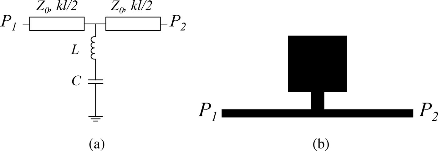
The hypothesis of the approach considered in this paper is that by truncating periodicity with unequal SISS loading in the cells, it is possible to generate independent transmission zeros and thus improve the rejection level and bandwidth of the stop band, as compared with previous periodic implementations. As anticipated in the introduction, the paper is focused on the design of 90° slow-wave transmission lines, profusely utilized in microwave engineering in devices such as power splitters/combiners and couplers. For the reasons explained before, the lines will be implemented by means of two 45° unit cells, each one loaded with a different SISS. Both unit cells must exhibit the required characteristic impedance at the design frequency f 0, i.e. Z 1 = Z 2 = Z B. Finally, to determine completely the parameters of the schematic of the unit cell, shown in Fig. 1, the slow-wave ratio, swr, must be set to a reasonable value (we will consider identical swr for both unit cells in this work, but this is not actually necessary). The design equations are as follows [Reference Martín2, Reference Coromina, Selga, Vélez, Bonache and Martín37]:
 $$\cos (\beta l) = \cos (kl)-\displaystyle{{B_pZ_0} \over 2}\sin (kl)$$
 $$Z_B = \displaystyle{{Z_0} \over {\sin \,(\beta l)}}\lpar {\sin (kl)-B_pZ_0{\sin}^2(kl/2)} \rpar $$
 $$swr = \displaystyle{{v_{\,pL}} \over {v_{\,po}}} = \displaystyle{{\omega /\beta} \over {\omega /k}} = \displaystyle{{kl} \over {\beta l}}.$$
Fig. 1. Schematic representation of the unit cell of the considered slow-wave structure (a) and typical layout (b).
From the previous equations, the electrical length, kl, and characteristic impedance, Z 0, of the host line, as well as the value of the loading susceptance, B p, can be univocally determined. Note that these values are identical for both cells. In equations (1)–(3), βl is the electrical length of the cell (45° in our case), l is the length of the host line of the unit cell, v pL and v po are the phase velocities of the loaded and unloaded line, respectively, and ω is the angular frequency. The loading susceptance, B p, is given by
 $$B_p{\rm}={\rm } \displaystyle{{C_i \omega_0} \over {{\rm 1\;\ -\ \;} L_i C_i \omega_0^{\rm 2}}} $$
with ω 0 = 2πf 0, whereas the transmission zero frequencies provided by the SISSs are
 $$f_{z,i}{\rm}={\rm } \displaystyle{{\rm 1} \over {{\rm 2\pi}\sqrt {C_iL_i}}} $$
where the sub-index i (with i = 1, 2) is used to distinguish the inductance, L i, and capacitance, C i, of both SISS. Thus, from equations (4) and (5), the elements values L i and C i are perfectly determined, provided the transmission zeros f z,i are set to a certain value (note that the susceptance B p, identical for both SISS, is determined from the solutions of equations (1)–(3)).
Concerning the position of the two transmission zeros, a trade-off is necessary; that is, if such transmission zeros are very close, significant rejection is expected in their vicinity, but in a narrower band, as compared with the case of significantly separated transmission zeros. However, if the transmission zeros are extremely separated, then the rejection level in between such zeros may be degraded. A priori, a reasonable choice may be to set the transmission zeros in the vicinity of the first and third harmonic frequencies (however, this aspect, will be justified next).
Let us consider the design of a 90° slow-wave transmission line impedance inverter (i.e. θ = 2βl = 90°) operating at f 0 = 1 GHz, with characteristic impedance of Z B = 35.35 Ω, and with a slow-wave ratio of swr = 0.5. Note that with this value of the swr, it is expected to reduce the length of the inverter by a factor of two (as compared with the ordinary counterpart). On the other hand, the value of the characteristic impedance is justified as this slow-wave-based inverter will be later applied to the design of a power splitter based on an impedance inverter with 35.35 Ω impedance. The transmission zeros are set to f z,1 = 4 GHz and f z,2 = 6 GHz, i.e. slightly above and below the first and third harmonic frequencies, respectively, of the inverter. With this choice, a good balance between stop band bandwidth and rejection is achieved. By choosing f z,1 and f z,2 closer to the first (at 3 GHz) and third (7 GHz) harmonic frequencies, the bandwidth is further improved, but the rejection level is degraded.
Solution of equations (1)–(5) provides the following values: kl = 22.5°, Z 0 = 73.61 Ω, L 1 = 0.69 nH, C 1 = 2.30 pF, L 2 = 0.30 nH, and C 2 = 2.38 pF. Figure 2 depicts the frequency dependence of the electrical length and characteristic impedance of the designed slow-wave artificial line, as well as the frequency response, inferred from the circuit simulation of the schematic using Keysight ADS. The reference impedance of the ports has been considered to be 35.35 Ω in order to easily verify that the required value of the characteristic impedance (Z B = 35.35 Ω) at f 0 is satisfied (it is indicated by the reflection zero at that frequency). It can be seen from Fig. 2 that the required electrical length at f 0 (θ = 90°) is also satisfied. Finally, the frequency response, with transmission zeros located at 4 and 6 GHz, exhibits a wide stop band with significant rejection level.
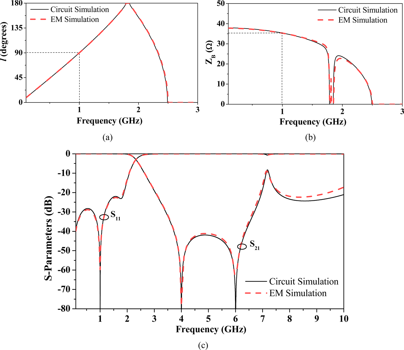
Fig. 2. Electrical length (a) characteristic impedance (b) and frequency response (c) of the designed 90° slow-wave transmission line, inferred from circuit simulation and lossless electromagnetic simulation.
Once the element values of the schematic have been inferred, we have generated the layout, where the SISS elements have been synthesized according to the method reported in [Reference Naqui, Durán-Sindreu, Bonache and Martín44]. The result can be seen in Fig. 3, where dimensions and the considered substrate are indicated. The response of this structure inferred from full-wave electromagnetic simulation (using Keysight Momentum) by excluding losses, is also depicted in Fig. 2. The excellent agreement between circuit and electromagnetic simulation is indicative of the validity of the SISS model and synthesis procedure.

Fig. 3. Layout of the designed SISS-loaded non-periodic slow-wave transmission line. Dimensions are W host = 0.23 mm, l host = 22.85 mm, W A,1 = 3.50 mm, l A,1 = 3.33 mm, W A,2 = 0.48 mm, l A,2 = 2.31 mm, W B,1 = 3.59 mm, l B,1 = 3.47 mm, W B,2 = 0.83 mm, l B,2 = 1.31 mm. The considered substrate is Rogers RO4003C with dielectric constant ε r = 3.55, thickness h = 0.203 mm, and loss tangent tanδ = 0.0022.
Application to a power splitter with filtering capability and experimental validation
The previously designed artificial line (inverter) has been applied to the implementation of a power splitter with filtering capability based on a 35.35 Ω impedance inverter with one input and two output 50 Ω access lines. This justifies the choice of the characteristic, or Bloch, impedance of the non-periodic slow-wave artificial line designed in the previous section. The photograph of the fabricated splitter is shown in Fig. 4 (the LPKF H100 drilling machine has been used for device fabrication).
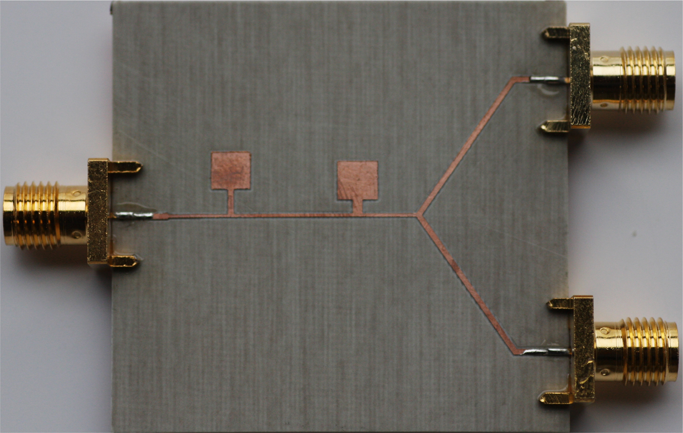
Fig. 4. Photograph of the fabricated power splitter with filtering capability, based on the designed non-periodic artificial line.
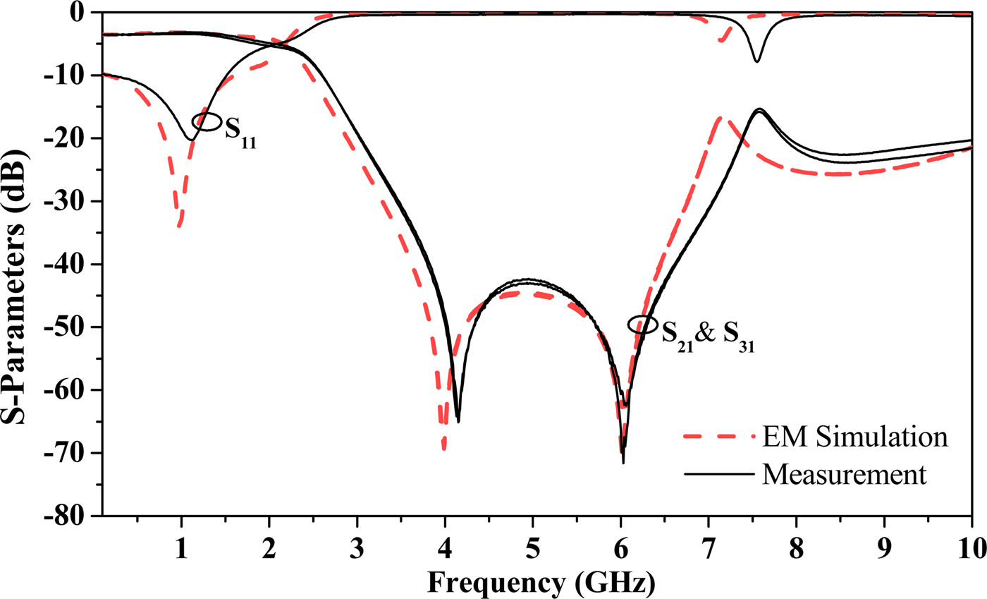
The measured frequency response of the splitter, inferred by means of the four-port Agilent PNA N5221A network analyzer is depicted in Fig. 5, where it is compared with the electromagnetic simulation by including losses. The reference impedance of the ports is 50 Ω, as usual, so that good matching at the design frequency is expected (note that with the impedance of the inverter set to 35.35 Ω, the impedance seen from the input port is 50 Ω, provided the output ports are terminated with matched loads). The slight disagreements between simulation and experiment are attributed to fabrication-related tolerances. The measured matching at the design frequency (1 GHz) is roughly S 11 = −20 dB, whereas power splitting has been found to be S 21 = −3.2 dB and S 31 = −3.4 dB (close to the ideal −3 dB value). It is also remarkable that the rejection level in the stop band is better than 20 dB between 3 and 7.4 GHz, and better than 15 dB between 3 GHz and at least 10 GHz, thereby efficiently suppressing at least the first four harmonic frequencies. This harmonic suppression represents a substantial improvement as compared with the structure reported in [Reference Coromina, Selga, Vélez, Bonache and Martín37], based on a pair of identical SISS-loaded cells. Finally, the length of the slow-wave inverter is 22.85 mm, i.e. roughly half the length of the inverter implemented by means of an ordinary line (44.5 mm), in agreement with the considered swr.

Fig. 5. Measured and simulated frequency response of the designed and fabricated power splitter with filtering capability.
The non-periodic slow-wave structure considered in this paper and the related application (power splitter with reduced dimensions and with harmonic suppression capability) can be categorized within the set of works devoted to the design of compact and harmonic suppressed planar microwave components based on slow-wave structures [Reference Chuang3–Reference Selga, Coromina, Vélez, Fernández-Prieto, Bonache and Martín39]. The main advantage and novelty of the reported approach is the fact that the slow-wave structure is based on reactive loading elements (SISS) that introduce transmission zeros in the stop band. Indeed, this aspect was already introduced in [Reference Coromina, Selga, Vélez, Bonache and Martín37], but in this paper periodicity has been truncated (yet keeping the slow-wave effect) by considering different SISSs, each one providing independent transmission zeros. The result is an improved stop band and an efficient harmonic suppression capability.
Although most works on harmonic suppressed compact devices based on slow-wave artificial lines are focused on couplers and filters, the design of power splitters has been also considered [Reference Scardelletti, Ponchak and Weller15, Reference Vélez, Selga, Bonache and Martín28, Reference Selga, Vélez, Bonache and Martín29, Reference Selga, Vélez, Bonache and Martín35–Reference Selga, Coromina, Vélez, Fernández-Prieto, Martínez-Ros, Bonache, Aznar-Ballesta and Martín36]. However, in such works, the loading elements, either inductances, capacitances, or a combination of both components, do not provide transmission zeros in the stop band. The exception is the splitter of [Reference Vélez, Selga, Bonache and Martín28], where a transmission zero is apparent, but not explained by the effects of reactive loading (nevertheless, the harmonic rejection efficiency of such splitter is not demonstrated in [Reference Vélez, Selga, Bonache and Martín28]). Much more efficient harmonic suppression is achieved with the approach reported in the present work. Indeed, in none of the works reported in [Reference Scardelletti, Ponchak and Weller15, Reference Vélez, Selga, Bonache and Martín28, Reference Selga, Vélez, Bonache and Martín29, Reference Selga, Vélez, Bonache and Martín35–Reference Selga, Coromina, Vélez, Fernández-Prieto, Martínez-Ros, Bonache, Aznar-Ballesta and Martín36] harmonic suppression better than 20 dB up to the fourth harmonic band (as demonstrated in the implementation of this paper) is achieved. Nevertheless, it is remarkable the size reduction capability of the splitter in [Reference Selga, Vélez, Bonache and Martín35] (with roughly 38% the size of the conventional counterpart), related to the simultaneous inductive and capacitive loading. In the device of this paper, as well as in those splitters reported in [Reference Vélez, Selga, Bonache and Martín28] and [Reference Selga, Vélez, Bonache and Martín29], the size reduction is roughly 50%, whereas in [Reference Scardelletti, Ponchak and Weller15, Reference Selga, Coromina, Vélez, Fernández-Prieto, Martínez-Ros, Bonache, Aznar-Ballesta and Martín36], the miniaturization capability is worst. Concerning matching (S 11) and power splitting (S 21, S 31), the results provided in the different works reveal that comparable magnitude levels for such parameters at the design frequency are obtained. Note that the main relevant aspect of the proposed approach is the fact that a significant harmonic suppression capability is achieved by virtue of the controllable transmission zeros.
Conclusion
In conclusion, it has been demonstrated in this paper that by implementing slow-wave transmission lines with non-periodic reactive loading, particularly using SISS, it is possible to enhance the stop band of the structure, and achieve an efficient harmonic suppression. We have designed a 35.35 Ω quarter-wavelength impedance inverter based on the SISS-loaded non-periodic transmission lines, which has been subsequently applied to the implementation of a power splitter. By controlling the position of the transmission zeros provided by the SISS, it has been possible to efficiently suppress up to the fourth harmonic with more than 20 dB rejection. By virtue of the slow-wave effect associated to reactive loading, the length of the constitutive impedance inverter of the splitter has been reduced by a factor of two as compared with the ordinary implementation.
Author ORCIDs
Jan Coromina, https://orcid.org/0000-0002-3541-4663
Acknowledgement
This work was supported by MINECO-Spain (projects TEC2016-75650-R and TEC2017-84724-P), Generalitat de Catalunya (projects 2017SGR-1159), Institució Catalana de Recerca i Estudis Avançats (who awarded Ferran Martín), and by FEDER funds. Paris Vélez also acknowledges Ministerio de ciencia, innovación y universidades through Juan de la Cierva fellowship, with reference IJCI-2017-31339.
 Jan Coromina was born in Barcelona, Spain, in 1989. He received the Bachelor's degree in Electronics Engineering for Telecommunication in 2014 and the Telecommunication Engineering Master's degree in 2017, both in Universitat Autònoma de Barcelona (UAB), Barcelona, Spain. He is currently carrying out his Ph.D. degree within the research center CIMITEC (Departament d'Enginyeria Electrònica) at the same university, on the field of microwave circuit design and miniaturization. Specifically, his work is focused on the design of slow-wave structures and their application to a diversity of microwave circuits. In 2016, he joined the company IDNEO Technologies as an RF Engineer, where he developed ISM antennas for industrial applications, and multi-service LNA for the automotive sector.
 Paris Vélez was born in Barcelona, Spain, in 1982. He received the degree in Telecommunications Engineering, specializing in electronics, the Electronics Engineering degree, and the Ph.D. degree in Electrical Engineering from the Universitat Autònoma de Barcelona, Barcelona, in 2008, 2010, and 2014, respectively. His Ph.D. thesis concerned common mode suppression differential microwave circuits based on metamaterial concepts and semi-lumped resonators. During the Ph.D., he was awarded with a pre-doctoral teaching and research fellowship by the Spanish Government from 2011 to 2014. From 2015 to 2017, he was involved in the subjects related to metamaterials sensors for fluidics detection and characterization at LAAS-CNRS through a TECNIOSpring fellowship cofounded by the Marie Curie program. His current research interests include the miniaturization of passive circuits RF/microwave and sensors-based metamaterials through Juan de la Cierva fellowship. Dr. Vélez is a Reviewer for the IEEE Transactions on Microwave Theory and Techniques and for other journals.
 Jordi Bonache was born in Cardona (Barcelona), Spain, in 1976. He received the Physics and Electronics Engineering degrees and the Ph.D. in Electronics Engineering from the Universitat Autònoma de Barcelona, in 1999, 2001, and 2007, respectively. In 2000, he joined the High Energy Physics Institute of Barcelona, where he was involved in the design and implementation of the control and monitoring system of the MAGIC telescope. In 2001, he joined the Department of Electronics Engineering, Universitat Autònoma de Barcelona, where he is currently a Professor of Electronics. From 2006 to 2009, he was an Executive Manager with CIMITEC, Bellaterra, Spain, where he is currently a Project Manager and leads the research on RFID and antennas. His current research interests include active and passive microwave devices, metamaterials, antennas, and RFID.
 Francisco Aznar-Ballesta was born in Granada, Spain, in 1978. He received the Electronics Engineering Degree from the Universidad de Granada (UGR) in 2005 and the Ph.D. degree in Electronics Engineering from the Universitat Autònoma de Barcelona (UAB) in 2009. After a postdoctoral stay in the Universidad Carlos III de Madrid (UC3M), he joined in 2012 the Universidad Politécnica de Madrid (UPM), where he is currently an Associate Professor. In 2013, he worked in the Institüt für Mikrowellentechnik und Photonik in the Tecknische Universität Darmstadt (TUD), within the José Castillejo MINECO Program. He is currently, a Collaborator Researcher in CIMITEC (Departament d'Enginyeria Electrònica) at UAB. His current research interests include design, miniaturization, and characterization of passive RF/microwave circuits and metamaterials-based sensors.
 Armando Fernández-Prieto was born in Ceuta, Spain, in 1981. He received the Licenciado and Ph.D. degrees in Physics from Universidad de Sevilla, Seville, Spain, in 2007 and 2013, respectively. During 2010–2011, he was a Visiting Researcher at Heriot-Watt University (Edinburgh, Scotland, UK), at Prof. Jiasheng Hong's group where he was involved in the design of multilayer LCP balanced microwave filters. He was also a visiting researcher in 2017 at Universidad Autónoma de Barcelona (Barcelona, Spain) at CIMITEC under the supervision of Prof. Ferran Martín. During this period, he was involved in the design of microwave sensors, slow-wave structures, and balanced-to-balanced planar diplexers. Nowadays, he is with the Departamento de Electrónica y Electromagnetismo, Universidad de Sevilla, Seville, Spain, where, in 2018, he became an Assistant Professor. His research interests focus on printed passive microwave components, sensors, and metamaterials. He is a Reviewer for the IEEE Transacttions on Microwave Theory and Techniques, IEEE Access, and IEEE Microwaves and Wireless Component Letters, as well as for many other journals.
 Ferran Martín was born in Barakaldo, Spain, in 1965. He received the B.S. degree in Physics and Ph.D. degree from the Universitat Autònoma de Barcelona (UAB), Barcelona, Spain, in 1988 and 1992, respectively. From 1994 to 2006 he was an Associate Professor in Electronics at the Departament d'Enginyeria Electrònica (Universitat Autònoma de Barcelona), and since 2007 he is a Full Professor of Electronics. His research activity has been very broad, including the modeling and simulation of electron devices for high-frequency applications, millimeter wave and THz generation systems, the application of electromagnetic bandgaps to microwave and millimeter wave circuits, and the application of metamaterial concepts to the miniaturization and optimization of microwave circuits and antennas. He is now very active in the development of microwave sensors for dielectric characterization and motion control, and also in the topic of chipless-RFID. He is the Head of the Microwave Engineering, Metamaterials and Antennas Group (GEMMA Group) at UAB, and Director of CIMITEC, a Research Center on Metamaterials supported by TECNIO (Generalitat de Catalunya). He has organized several international events related to metamaterials, including Workshops at the IEEE International Microwave Symposium (years 2005 and 2007) and European Microwave Conference (years 2009, 2015, 2017, and 2018), and the Fifth International Congress on Advanced Electromagnetic Materials in Microwaves and Optics (Metamaterials 2011), where he has acted as Chair of the Local Organizing Committee. He has acted as a Guest Editor in several Special Issues, mainly related to Metamaterials, in various International Journals. He has authored and co-authored over 580 technical conference, letter, journal papers, and book chapters, he is co-author of the book on Metamaterials entitled Metamaterials with Negative Parameters: Theory, Design and Microwave Applications (John Wiley & Sons Inc. 2008), author of the book Artificial Transmission Lines for RF and Microwave Applications (John Wiley & Sons Inc. 2015), co-editor of the book Balanced Microwave filters (John Wiley & Sons Inc. and IEEE-Press 2018), and he has generated 19 Ph.D.s. Ferran Martín has filed several patents on metamaterials and has headed several Development Contracts. Prof. Martín is a member of the IEEE Microwave Theory and Techniques Society (IEEE MTT-S). He is a Reviewer of the IEEE Transactions on Microwave Theory and Techniques and IEEE Microwave and Wireless Components Letters, among many other journals, and he serves as member of the Editorial Board of IET Microwaves, Antennas and Propagation and International Journal of RF and Microwave Computer-Aided Engineering. He is also a Member of the Technical Committees of the European Microwave Conference (EuMC) and International Congress on Advanced Electromagnetic Materials in Microwaves and Optics (Metamaterials). Among his distinctions, Ferran Martín has received the 2006 Duran Farell Prize for Technological Research, he holds the Parc de Recerca UAB – Santander Technology Transfer Chair, and he has been the recipient of two ICREA ACADEMIA Awards (calls 2008 and 2013). He is a Fellow of the IEEE since 2012 and a Fellow of the IET since 2016.