I. INTRODUCTION
Self-complementary antenna has become very popular among the researchers due to the broadband nature of its radiation characteristics. Self-complementary concept is widely exploited to realize miniaturized ultra-wideband (UWB) antenna [Reference Mushiake1–Reference Liu, Cheung and Yuk3]. The input impedance of such type of antenna is generally characterized by its constant input impedance of 188.5 Ω. In spite of all the impressive aforementioned prospects, an additional impedance matching circuit is required to transform input impedance from 188.5 to 50 Ω in order to make it integrated with the RF front end [Reference Guo, Chen and Parini4–Reference Lin, Huang and Su7]. In previous literatures, several types of self-complementary or quasi-self-complementary configuration have been explained for UWB application, such as half circular disk types [Reference Guo, Wang, Gao, Wang, Chen and Parini8], stepped triangular type [Reference Abd El-Hameed, Salem, Abdallah and Hashish9], rectangular type [Reference Huang and Chen10], fractal BOW-TIE type [Reference Sayidmarie and Fadhel11], circular disk type [Reference Sayidmarie and Fadhel12], crossbar fractal type [Reference Abd El-Hameed, Salem, Abdallah and Hashish13], horn-shaped self-complementary structure [Reference Alomainy, Hao, Parini and Hall14]. In this article, a novel design of microstrip line-fed quasi-self-complementary semi-octagonal band-notched UWB antenna is explained. The distinctive feature of this proposed design is the excellent impedance matching improvement capability, especially for the lower frequency matching by using effective truncation on the ground plane. The remarkable principle of self-complementary antenna ensures the better reduction of the imaginary part of antenna impedance, which enhances traveling wave mode radiation and improves the impedance matching especially at higher frequency band. Therefore, it can be used for extremely broadband characteristics with reasonable radiation pattern. However, since self-complementary mirror image slot needs to be truncated on a finite ground plane, the lower limit of the bandwidth raises to a higher frequency. Furthermore, the input impedance transformation from 188.5 to 50 Ω by using complicated matching network will further narrow the bandwidth and limit the reduction of antenna size. The proposed design methodology is new in comparison to the previously reported work and our design is aimed to overcome the above drawbacks. Basic idea of semi-octagonal self-complementary structure has been chosen as initial configuration due to its fairly compact size (26 × 36.6 mm) and simple shape compared with irregular and complicated shape (as discussed in previous literatures [Reference Liu, Wang, Yin and Ren2–Reference Alomainy, Hao, Parini and Hall14]). This kind of structure is able to reduce the influence of the discontinuity present in the antenna feeding point, which gradually changes the distribution of the current flowing from the feeding line to the radiant patch. This effect consequently smoothens the electric current distribution on the patch surface and improves the impedance matching. On the other hand in semi-octagonal slotted counterpart, smoothness of the magnetic current distribution fully supports traveling waves at higher frequency. However, for lower impedance matching step-by-step ground plane etching process is adopted for the matching of lower edge of the operating bandwidth. The sequential truncation on ground plane of the proposed antenna definitely has a pronounced effect on the impedance matching, which contributes to minimize the lower cutoff frequency and makes antenna inherently suitable for extremely wideband operation (2.9–20 GHz). Another significance of the proposed design regarding band rejection capability is the quality factor (Q-factor) control of the WLAN rejection band (5.15–5.825 GHz), which is realized by inclusion of a new capacitive coupling mechanism by embedding a spiral-shaped, open-ended, quarter wavelength stub near the slotted periphery to the lower edge of the ground plane. In most of the early works, band-notched characteristics are realized by introducing various types of resonators to the UWB antenna. Previous literatures have mainly focused on the tuning control of central rejection frequency in those designs; however, sharpness of rejection bandwidth or frequency selectivity of the rejection band can hardly be controlled. A new capacitive coupling scheme has been proposed in this work to realize controllable rejection bandwidth at the targeted notch frequency. Sharpness control of notched band strongly related to the Q-factor improvement. Owing these above noticeable characteristics, this newly proposed design is the most promising candidate for narrow band WIMAX application (3.3–3.8 GHz), UWB wireless communication system, X band (8–12 GHz) and Ku band (12–18 GHz) satellite communication systems.
The equivalent circuit model is used to analyze the resonance behavior of quarter wavelength open stub. Apart from the frequency domain analysis, the time domain performance of the proposed antenna is also estimated to access its suitability in the wireless communication.
II. ANTENNA DESIGN AND ANALYSIS
A) Design of quasi-self-complementary UWB antenna
The development of the proposed UWB antenna (fabricated on FR-4 substrate with relative permittivity 4.4 and thickness 1.6 mm) has been carried out by four sequential design modifications as shown in Fig. 1. Initially in antenna-1, a half-shaped regular octagonal patch has been introduced with a mirror image slotted counterpart on the ground plane which relies on self-complementary geometry. In the next step, in antenna-2, an additional rectangular slot is etched in the ground plane. Furthermore, in antenna-3, a stepped rectangular slot is proposed for enhancement of electromagnetic coupling between the ground plane and the radiating element. Finally, in antenna-4, the top edge of the ground plane has been removed up to the optimum length to achieve the enhanced impedance matching for the lower frequency range of UWB.

Fig. 1. Design steps of proposed quasi-self-complementary semi-octagonal UWB antenna.
B) Design of quasi-self-complementary band-notched UWB antenna
Figure 2 illustrates the proposed band-notched UWB antenna. A quarter wavelength, open-ended spiral stub has been connected to the ground plane inside the slotted matching circuit of the UWB antenna to realize stop-band effect at 5.5 GHz. The length of the spiral-shaped metal strip has an inductive effect, and the electrical coupling between the turns of the spiral gives a capacitive effect. The coupling between the resonator and the truncated peripheries of ground plane gives rise to the capacitive effect and offers parallel resonance circuit. At 5.5 GHz, the resonance frequency of the proposed band-notched UWB can be empirically approximated as
 $$f_n = \displaystyle{c \over {4L_n \sqrt {\varepsilon _{reff}}}}, $$
where εreff = (εr + 1/2) and L n = X 1 + X 2 + X 3 + X 4 + X 5 + X 6 − 5t.

Fig. 2. Geometry and dimension of the proposed band-notched quasi-self-complementary UWB antenna.
C) Equivalent circuit model
The comprehension of this rejection mechanism can be assisted by the illustration and explanation of the surface current distribution. Due to the existence of spiral stub, little amount of current exists on ground plane at central rejection frequency because open-circuited stub draws more current by presenting low impedance at its anchor. The additional current path can be introduced to provide an adequate amount of capacitive coupling between the resonator and truncated periphery of the ground plane which offers parallel resonance band stop function. Coupling gap between the resonator and the ground plane plays a crucial role in the controlling of rejection bandwidth which is strongly related to control the Q-factor of rejection band response. The coupling gap between the ground plane and spiral-shaped stub is principally capacitive. A closer gap between the truncated edge of the ground plane and the spiral stub produces the strong amount of coupling. This in turn increases the surface current concentration as well as the stored energy around the spiral resonator and improves further the frequency selectivity and Q-factor of the rejection band. The stub connected to the ground plane produces parallel resonance effect. The conceptual equivalent circuit model of the proposed band-notched UWB antenna is shown in Fig. 3(a) where a parallel RLC resonant circuit corresponding to central rejection frequency of WLAN-notched band (5.5 GHz) is connected in series with Z A, which is the input impedance of UWB antenna. The effective input impedance of the proposed band-notched UWB antenna
 $$Z = Z_A + Z_n$$
here the notch impedance
 $$Z_n = \displaystyle{1 \over {(1/R_s ) + (1/j\omega L_s ) + j\omega C_s}}$$
according to Ref. [Reference Dong, Hong, Kuai and Chen15] resonance frequency and 3 dB notched bandwidth can be predicted as
 $$\omega _n = \displaystyle{1 \over {\sqrt {L_s C_s}}} $$
and
 $$\; \; \; \; \; \; \; \; \; BW_n = \displaystyle{1 \over {R_s C_s}}. $$
The real and imaginary parts of the input impedance (predicted by the HFSS simulator) have been plotted on Figs 3(b) and 3(c), respectively. It is observed that Re [Z] varies around 50 Ω and Im [Z] is varying around zero except the WLAN frequency band. Since Q-factor of the rejection characteristics of WLAN frequency band
 $$Q_n = \displaystyle{{\omega _n} \over {BW_n}} = R_s \sqrt {\displaystyle{{C_s} \over {L_s}}} \; $$
Hence  $ Q_n \propto \sqrt {(C_S /L_S )} $ consequently, it can be concluded that the Q-factor of the rejection band can be controlled by maintaining the gap between the resonator and the ground plane. Closer gap between the spiral-shaped stop-band element and the truncated part of the ground plane raises capacitive effect, which further improves the rejection band Q-factor Q n and decreases the notched bandwidth.

Fig. 3. (a) Equivalent circuit model of the proposed band-notched UWB antenna, (b) simulated impedance (real part), (c) simulated impedance (imaginary part).
III. RESULTS AND DISCUSSION
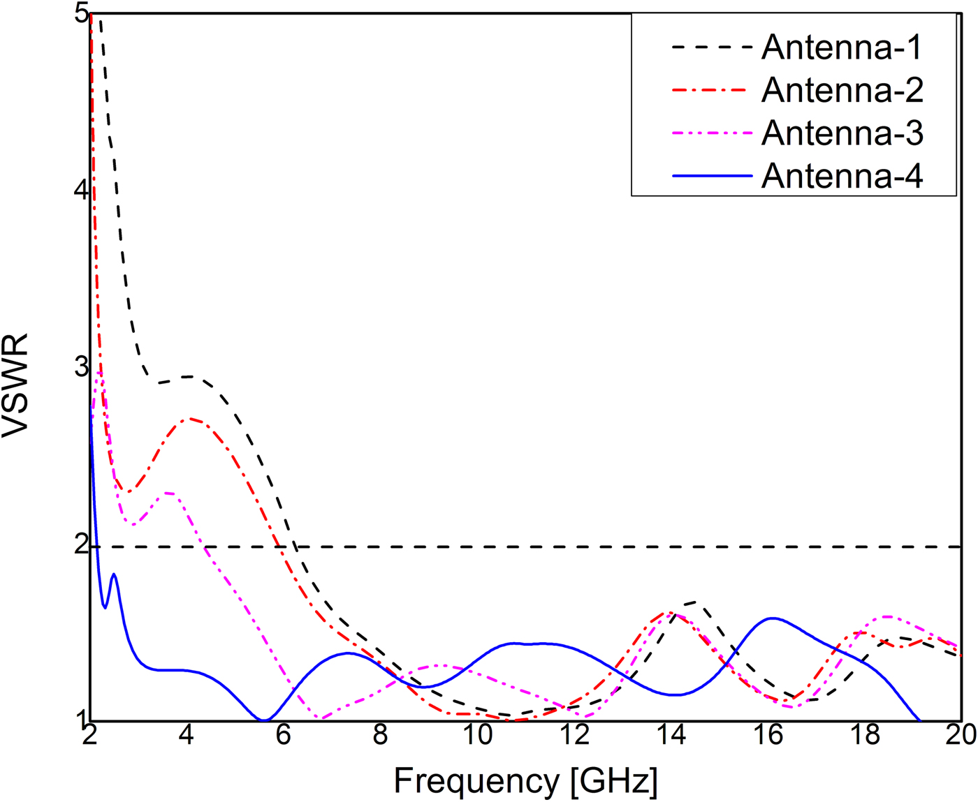
A) Comparative VSWR characteristics of antenna-1 to antenna-4
The simulated VSWR characteristics for the four antennas are plotted in Fig. 4. The gradual improvement of impedance bandwidth from antenna-1 to antenna-4 has the significance in changing the lower limit of the frequency band. For antenna-1, the complementary structure raises the limit of the higher frequency band up to 20 GHz, but the lower frequency limit fails to achieve the required UWB characterization. In antenna-2, the ground plane slot shifts the lower limit to 5.85 GHz, but still without sufficient UWB performance. In antenna-3, the stepped matching slot provides better impedance matching and finally antenna-4 fulfills the required UWB performance of the bandwidth which is extended from 2.65 to more than 20 GHz.

Fig. 4. VSWR against frequency for the four antennas shown in Fig. 1.
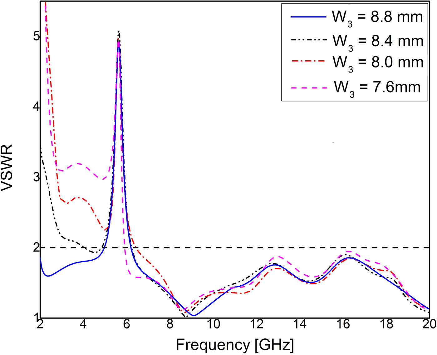
B) Variation of W 3 in proposed band-notched UWB antenna
W 3 is a major parameter for impedance matching. As W 3 decreases, the upper periphery of the ground becomes wider which significantly affects the impedance matching performance and lower limit of the UWB frequency band. On the other hand, the band rejection characteristics at 5.5 GHz is insensitive to the changing of W 3 as shown in Fig. 5.

Fig. 5. VSWR against frequency for different values of W 3.
C) Variation of W 1 in proposed band-notched UWB antenna
W 1 is the critical parameter to control the sharpness of rejection frequency band. As W 1 increases, the rapid decreases in capacitive effect due to the wider gap between the truncated part of the ground plane and spiral stub produces wider rejection bandwidth and low Q-factor. Besides, the deformation of the matching circuit creates a slight impedance mismatch between the ground plane and radiating element at higher frequency range as shown in Fig. 6.
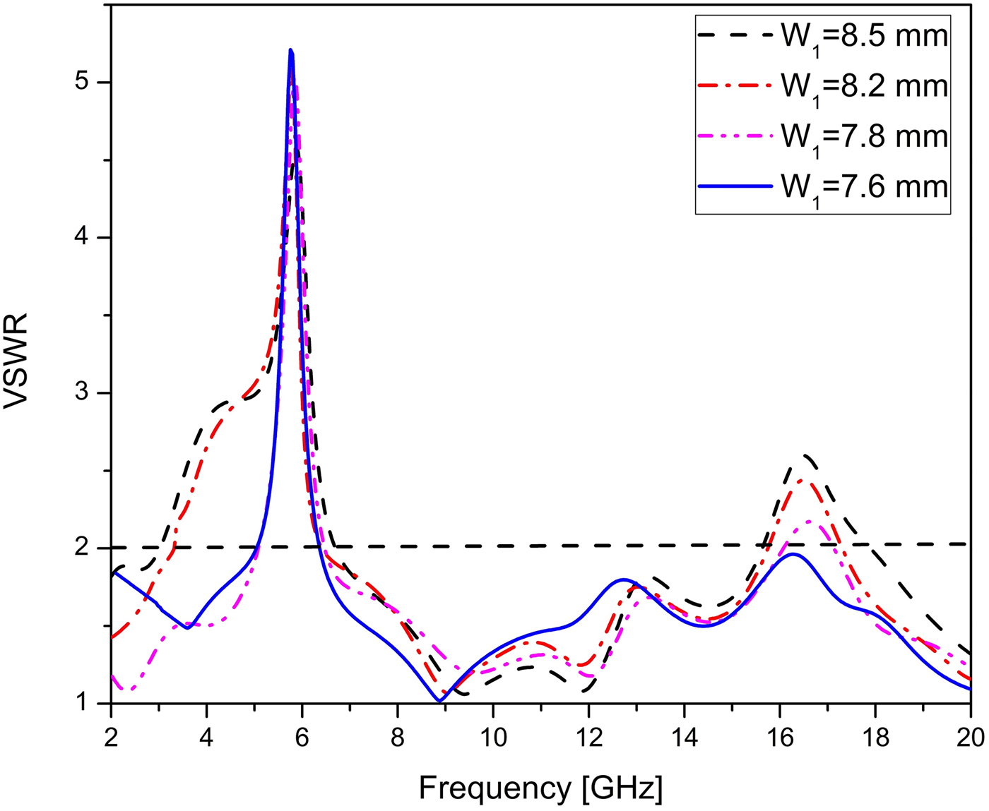
Fig. 6. VSWR against frequency for different values of W 1.
D) Variation of L 2 in proposed band-notched antenna
The gap L 2 between slotted part of the ground plane and the band rejection element is a crucial parameter to control the Q-factor of the rejection band. As L 2 increases, the effective capacitance decreases which results for the wider bandwidth of the rejection band and the Q-factor becomes lower as shown in Fig. 7.
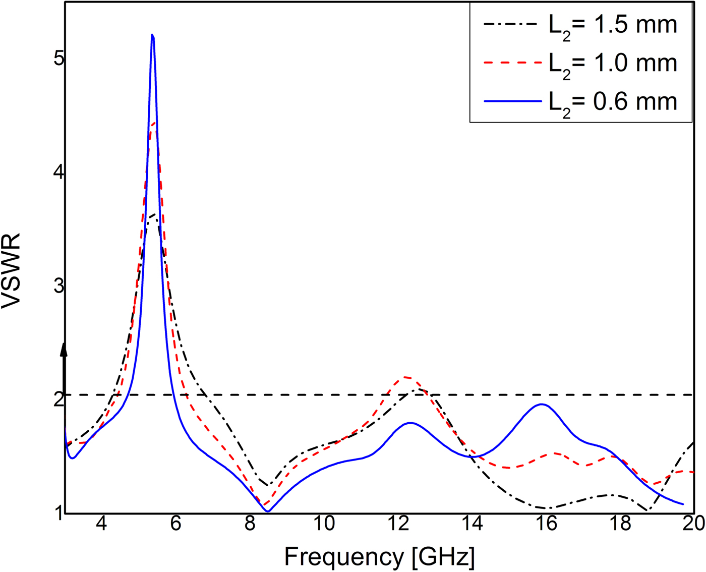
Fig. 7. VSWR against frequency for different values of L 2.
E) Variation of W 2 in proposed band-notched antenna
The variation of VSWR performance of the proposed band-notched UWB has been illustrated in Fig. 8. Decreasing the value of W 2 reduces the effective length of the spiral-shaped resonator. This ultimately increases the rejection frequency. Another important point regarding the variation of W 2 can be mentioned that if W 2 increases, surface currents get more concentrated at the resonator, which is analogous to the high perturbation and significant signal drop across the combination in a series-resonant band-stop filter at a stop-band resonance. This phenomena lead to the improvement of notch VSWR.
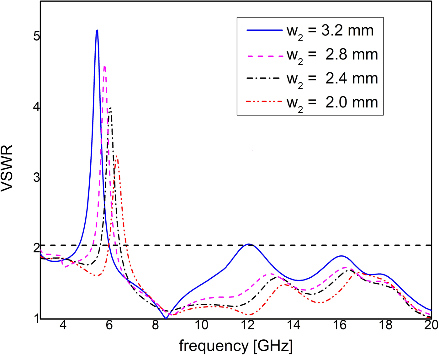
Fig. 8. VSWR against frequency for different values of W 2.
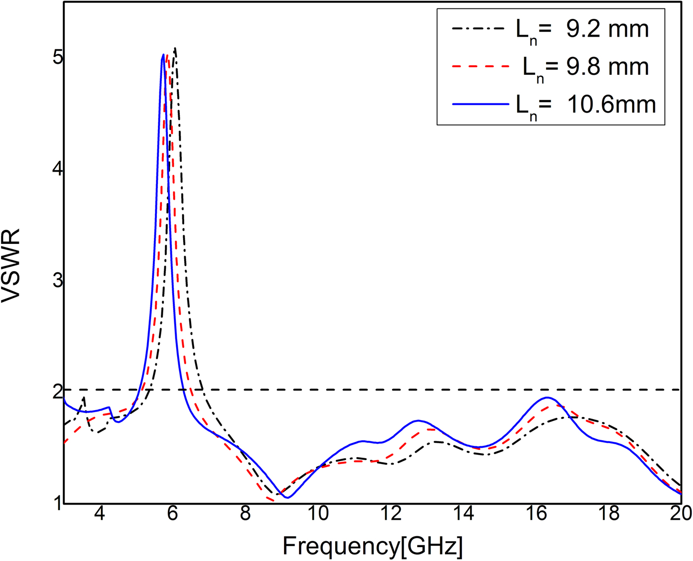
F) Variation of L n in proposed band-notched antenna
Effective length of the rectangular spiral stub to the ground plane has the major role in tuning characteristics of the proposed band-notched UWB antenna. As the stub length is reduced, the rejection frequency increases as shown in Fig. 9.

Fig. 9. VSWR against frequency for different values of L n.
G) Simulated surface current distribution
The simulated surface current distribution of the proposed band-notched UWB antenna is displayed for different pass-band and stop-band frequencies as shown in Fig. 10 at the stop-band resonance frequency (5.5 GHz); strong coupled surface current can be observed around the spiral stub, which makes the antenna non-responsive. This is analogous to the signal drop across parallel RLC combination at the resonance. However, for the different pass-band frequencies, spiral-shaped resonator does not work and the antenna returns to the normal operation. As observed in Figs 10(c) and 10(d) for the pass-band resonance at 9 and 14.5 GHz, a surface current is mainly distributed on the edges of semi-octagonal truncated part of the ground plane, which ensures the promising prospect with broadband characteristics of proposed self-complementary design.

Fig. 10. Simulated surface current distribution for the proposed band-notched UWB antenna on the ground plane at (a) 3.5 GHz, (b) 5.5 GHz, (c) 9 GHz, (d) 14.5 GHz.
H) Experimental verification
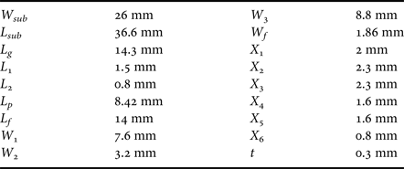
The optimum dimension of the proposed UWB antennas with and without band-notched characteristics has been summarized in Table 1 and prototypes are illustrated in Fig. 11. The simulated and measured VSWR performances for the proposed quasi-self-complementary UWB antenna with and without band-notched characteristics are illustrated in Fig. 12. A good agreement regarding notch frequency band with little disagreement in the lower cutoff frequency has been observed successfully. The measured frequency range (VSWR < 2) is from 2.9 to 20 GHz except for the stop band of 5.15–5.825 GHz.

Fig. 11. Fabricated structure of (a) proposed UWB antenna, (b) proposed band-notched UWB antenna.
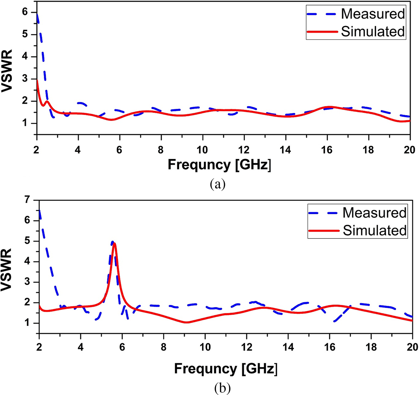
Fig. 12. Simulated and measured VSWR of (a) proposed UWB antenna, (b) proposed band-notched UWB antenna.
Table 1. Optimized parameter value of the proposed antenna shown in Fig. 2.

I) Measured far-field radiation pattern
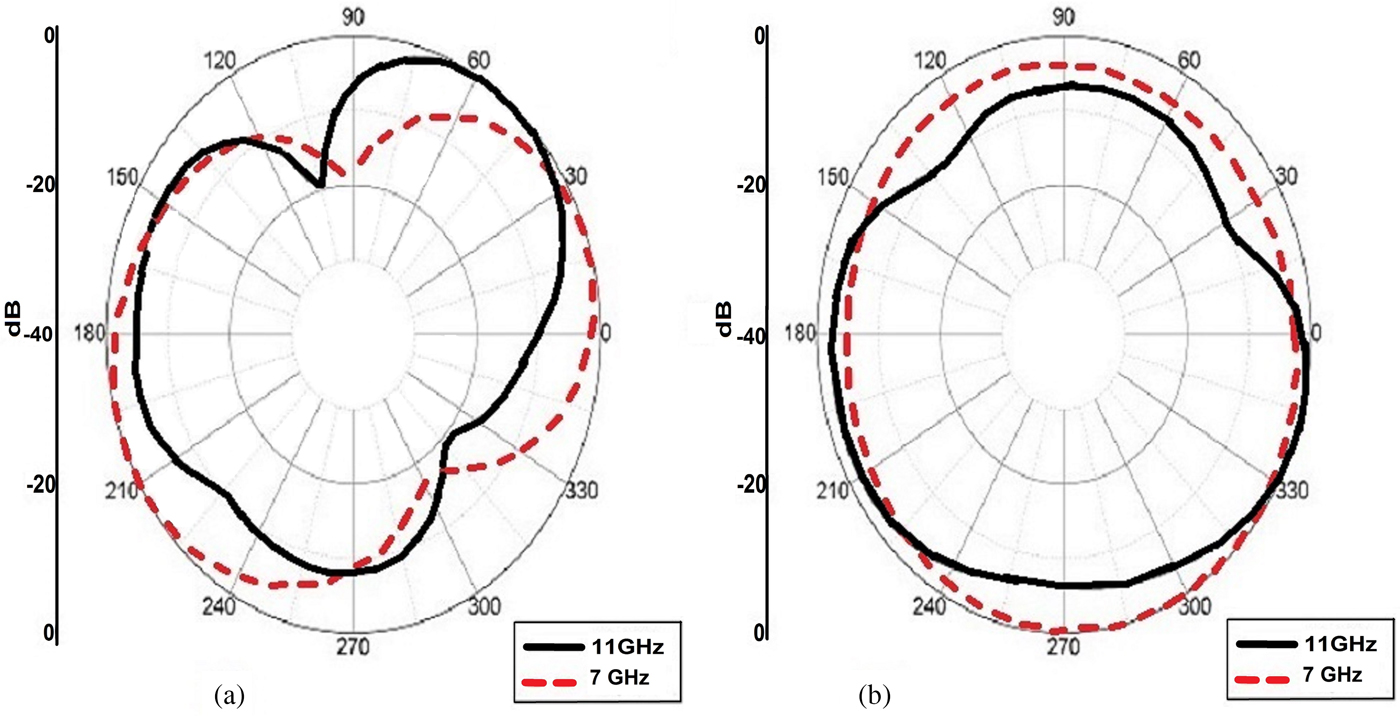
The co-polar E- and H-plane radiation patterns of the proposed band-notched UWB antenna are illustrated in Fig. 13 at 7 and 11 GHz. The E-plane pattern at 7 GHz is monopole-like, whereas the H-plane patterns are quasi-omnidirectional.

Fig. 13. Measured radiation patterns: (a) E-plane, (b) H-plane.
J) Measured peak gain
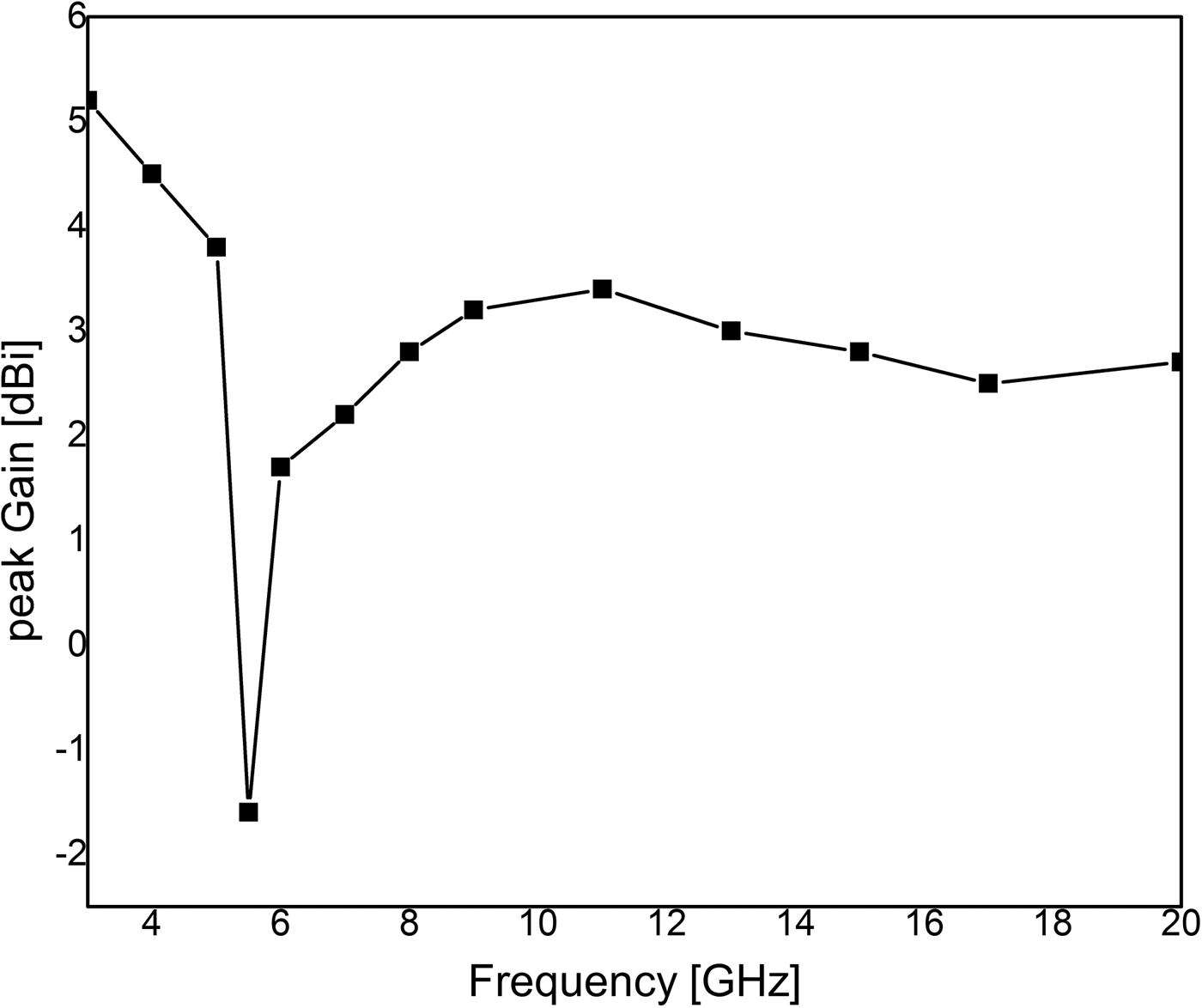
Figure 14 illustrates the measured peak gain response of the proposed band-notched UWB antenna throughout the operating frequency. It is clearly observed that peak gain sharply dips down at 5.5 GHz.

Fig. 14. Measured gain of the proposed band-notched UWB antenna.
IV. GROUP DELAY AND TIME DOMAIN PERFORMANCE
A) Group delay
Group delay is a measure of the signal transition time through a device and is defined as the negative rate of change of phase with frequency. The characteristic of the group delay indicates the phase linearity of the antenna in the far field. In the pass band, a pulse signal is not distorted between transmitting and receiving antenna. Phase is almost linear with respect to frequency and group delay has slightly small variation. At notch frequency, band degree of distortion becomes higher which leads to the phase non-linearity and group delay variation deteriorates. Group delay of the proposed band-notched UWB antenna has been investigated in face-to-face and side-by-side orientation by keeping a pair of proposed antennas at a distance of 120 mm from each other as shown in Fig. 15. In both the orientations, a sharp group delay > 1 ns can be observed at the rejection frequency of 5.5 GHz due to phase non-linearity. However, the group delay variation is negligible for the entire operating band (2.9–20 GHz).
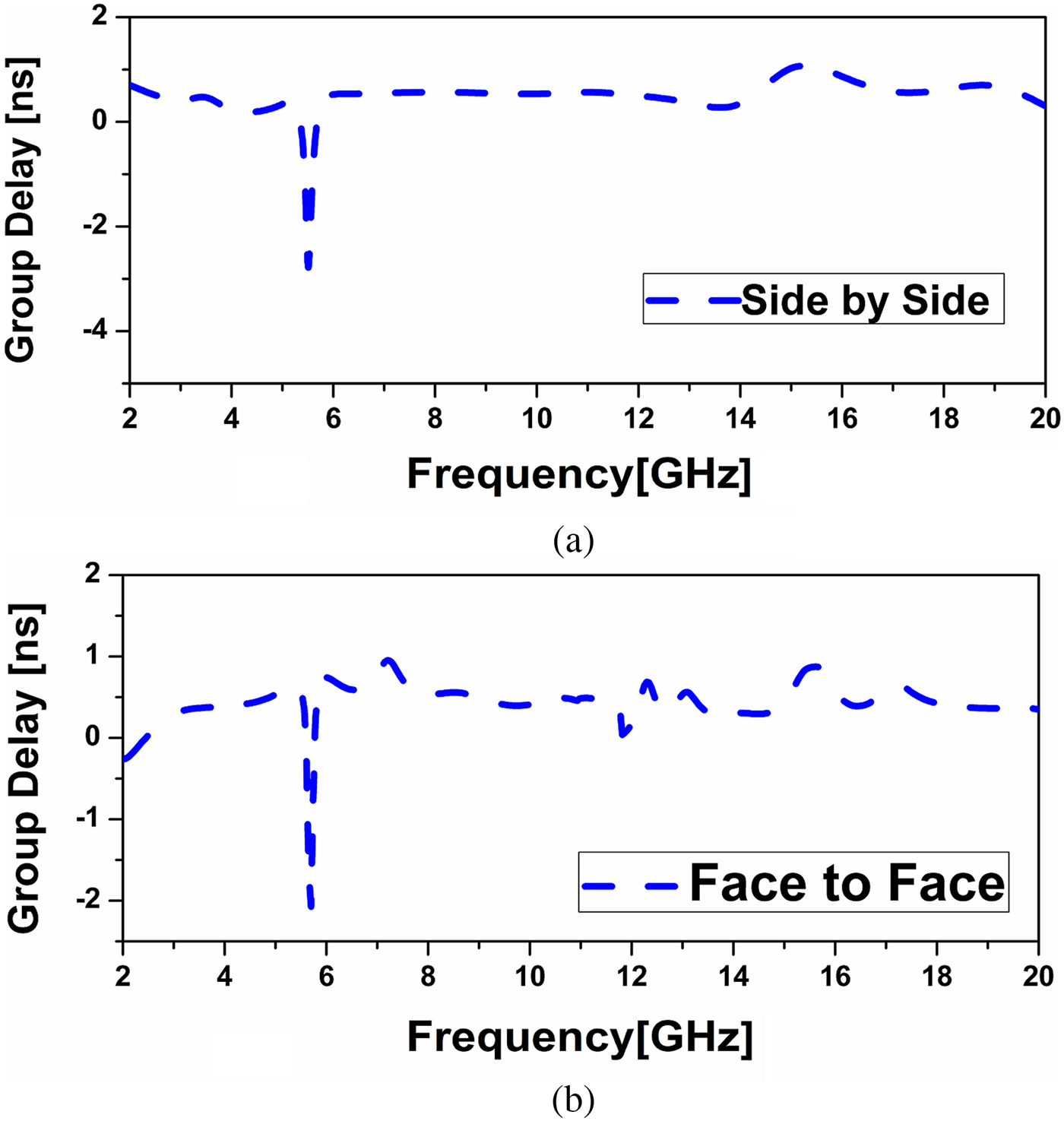
Fig. 15. Group delay of the proposed band-notched UWB antenna: (a) face-to-face, (b) side-by-side.
B) Pulse distortion and fidelity factor
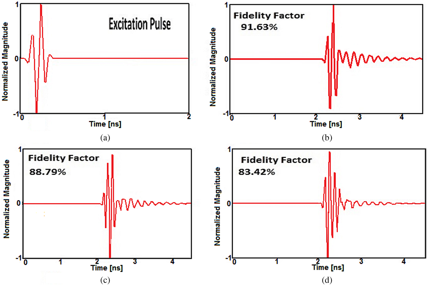
Since UWB systems use pulse transmission, hence it becomes necessary to investigate how much distortion of the pulse occurs for the proposed antenna. The fidelity factor is one of the important parameters, which can measure the pulse preserving capability of the antenna. If p(t) and r(t) are the transmitting and received pulses, then the fidelity factor (FF) can be defined as
 $$FF = \mathop {\max} \limits_\tau \left\{ {\displaystyle{{\int\!P\left( t \right)r\left( {t - \tau} \right)dt} \over {\sqrt {\int\!p^2 \left( t \right)dt} \sqrt {\int\!r^2 \left( t \right)dt}}}} \right\}.$$
As observed from Fig. 16 that ringing is lowest and fidelity factor is highest at θ = 00 and ϕ = 900 as compared with the other two cases. However, FF for different angles exhibits satisfactory results, which ensure the pulse preserving capability of the proposed band-notched UWB antenna.

Fig. 16. (a) Transmitting antenna input, and received far-field signals by virtual probes for ϕ = 90° and varying θ in the E-plane: (b) θ = 0°, (c) θ = 45°, (d) θ = 90°.
V. CONCLUSION
A quasi-self-complementary half-octagonal UWB antenna with band rejection characteristics at 5.5 GHz has been designed and investigated. To accomplish the improvement of impedance matching, particularly for the lower frequency band of UWB range, step-by-step modification of the ground plane has been realized by cutting different rectangular slots. To mitigate the WLAN (5.15–5.825 GHz) band interference, a quarter wavelength spiral stub has been introduced inside the truncated matching circuit of the ground plane. The gap between the rectangular spiral and edge of the truncated periphery of the ground plane has a wide control range of rejection bandwidth. The measured operating bandwidth of the proposed antenna is 2.9–20 GHz with rejection band of 5.15–5.85 GHz. The input impedance and simulated surface current are used to analyze the band rejection capability of the rectangular spiral stub.
 Mr. Rajarshi Sanyal has obtained his AMIETE and M.Tech degrees in Electronics and Communication. His area of research includes microstrip antenna and microstrip filters. Presently he is associated with the MCKV Institute of Engineering as an Assistant Professor. He has presented and published various research papers in national and international journals.
 Prof. (Dr.) Partha Pratim Sarkar obtained his M.E. and Ph.D. degrees in Engineering from the Jadavpur University in the years 1994 and 2002, respectively. He earned his B.E. degree in Electronics and Telecommunication Engineering from the Bengal Engineering College (presently known as IIEST, Shibpur) in the year 1991. He is presently working as a Professor at the Department of Engineering and Technological Studies, University of Kalyani. His area of research includes microstrip antenna, microstrip filter, frequency selective surfaces, and artificial neural network. He has contributed to numerous research articles in various journals and conferences of repute. He is also a Life Fellow of IETE (India) and IE (India).
 Prof. (Dr.) Santosh Kumar Chowdhury obtained his M.E. and Ph.D. degrees in Engineering from the Jadavpur University in the years 1968 and 1971, respectively. He earned his B.E degree in Electronics and Telecommunication Engineering from the Jadavpur University in the year 1964. He is a Senior Member of IEEE, Life Fellow of IETE, Fellow of IE, Fellow of West Bengal Academy of Science and Technology. His area of research includes microstrip antenna, microstrip filter, and frequency selective surfaces. He has contributed more than 50 international research articles in various journals and conferences of repute.