


Introduction
Multi-antennas are widely used in modern communication devices to improve performance of the wireless systems. As compared to the multi-antenna system, the multiband operation scale down the number of resonating elements, hardware complexity, design time, and overall cost. A multiband behaviour can be obtained by introducing slots on the radiator or ground surface. Recently, circularly polarized (CP) antennas received considerable attention from designers as they encounter multipath fading effects and polarization mismatch losses. In the literature, various CP antenna designs have been suggested for multiband function [Reference Beddeleem, Ribero, Kossiavas, Staraj and Fond1–Reference Dardeer, Elsadek and Abdallah24]. In [Reference Beddeleem, Ribero, Kossiavas, Staraj and Fond1], a dual-band CP antenna was developed with two imbricating patches. However, the alignment of the two patches is difficult in this antenna design. Dual-band stacked patch antennas with probe feed [Reference Nayeri, Lee, Elsherbeni and Yang2] and hybrid feed [Reference Yang and Row3] were presented for circular polarization. But, the dual-band performance was achieved at the cost of design complexity. Single-layered dual-band CP antenna with concentric annular rings [Reference Bao and Ammann4] and capacitively coupled annular-ring slot antenna [Reference Wang, Li, Zhang, Joines and Liu5] were reported. A patch antenna with a truncated corner was presented [Reference Pyo and Shin6], where an arrow-shaped triangular stub was loaded on the patch for polarization agility. An L-shaped slot antenna was proposed with metasurface [Reference Cao, Zhang, Hong and Jin7]. However, the extra layer changed the profile of the antenna.
A probe-fed dual-band CP antenna with four sequentially rotated shorted monopoles and a U-slot was presented [Reference Wang, Zhu, Guo and Wu8]. Since the antenna employed vias, drilling is needed, therefore, it could be difficult to integrate on the printed circuit board (PCB). A dual-band dual-polarized antenna with D-shaped complementary split-ring resonator (CSRR) engraved on the ground surface was proposed [Reference Singh, Kanaujia, Pandey, Gangwar and Kumar9]. A tapered microstrip line-fed hexagonal slot antenna was proposed with three L-shaped slits for wireless and satellite applications [Reference Baek and Hwang10]. A trident-shaped dipole antenna was presented for 2.4/5.2/5.8 GHz WLAN applications [Reference Ta, Park and Ziolkowski11], where the antenna was backed with high impedance surface (HIS). A triple-band CP antenna was proposed with two electromagnetically coupled radiating elements [Reference Bao and Ammann12]. Planar triple-band CP monopole antenna designs with different slots were reported in [Reference Xu, Li, Q, Yang and Yang13, Reference Hoang and Chang Park14]. A tri-band monopole antenna was proposed with a Y-shaped radiator for WLAN and Wi-MAX [Reference Wu, Shi, Li and Bai15]. The antennas were loaded with the split-ring resonator (SRR) for obtaining multiple CP bands [Reference Kandasamy, Majumder, Mukherjee and Ray16–Reference Tharehalli Rajanna, Rudramuni and Kandasamy18]. A dual-band slot antenna was presented with extended corners and an array of inclined strips [Reference Paul, Kandasamy and Sharawi19]. A coplanar waveguide (CPW)-fed broadband CP antenna was developed in [Reference Jaiverdhan, Sharma and Yadav20], where rectangular, L-, and spiral slots were embedded in the antenna for circular polarization. A multi-polarized triple-band antenna was developed in [Reference Agrawal, Gautam and Rambabu21], where asymmetric slots were loaded on the patch for achieving circular polarization. Dual-band single-layered antennas loaded with inverted L- and U-shaped strips were reported [Reference Weng, Sze and Chen22,Reference Dardeer, Elsadek, Abdallah and Elhennawy23]. In [Reference Dardeer, Elsadek and Abdallah24], a 2 × 2 array of CP antenna elements was presented for IoT systems. However, the array used a complex sequential feeding mechanism. The antennas in [Reference Nayeri, Lee, Elsherbeni and Yang2, Reference Yang and Row3, Reference Baek and Hwang10, Reference Ta, Park and Ziolkowski11, Reference Bao and Ammann12] showed complex multi-layered geometry, therefore integration of such antennas into the PCB is difficult. The antenna sizes were relatively larger in [Reference Wang, Li, Zhang, Joines and Liu5, Reference Wang, Zhu, Guo and Wu8, Reference Bao and Ammann12, Reference Wu, Shi, Li and Bai15, Reference Tharehalli Rajanna, Rudramuni and Kandasamy18, Reference Jaiverdhan, Sharma and Yadav20], therefore occupy more space, and this may also limit their integration with modern portable devices. The radiator designs in [Reference Paul, Kandasamy and Sharawi19–Reference Agrawal, Gautam and Rambabu21] were complex as they required an array of inclined strips and symmetric/asymmetric slots.
In this paper, a miniaturized, low-profile, single-feed multiband design composed of a microstrip-line inset-fed rectangular patch and a defected ground plane is presented. The multiband behaviour is obtained by introducing a modified electric−inductive−capacitive (m-ELC) resonator in the ground surface and a rotated rectangular groove in the patch. The antenna resonates at 2.2, 2.78, 3.18 and 3.82 GHz. For obtaining circular polarization, two square-shaped slots are engraved from the ground plane, and an arrow-shaped stub is introduced on the truncated patch of the antenna. Manufacturing of the prospective quad-band radiator is easy as it does not engage multiple feeds or special type of feeding method, vias, or stacked patches. The main contributions of the presented work are:
• The proposed antenna is a single-layered planar design, which offers easy integration with the PCB of the communication system.
• In the proposed multiband antenna, three CP bands are obtained without using a dual-feed or feeding network, therefore simplifying the antenna design procedure.
• The total area occupied by the prospective multiband antenna is comparatively small, and it can be easily integrated into portable RF devices.
• Most of the CP antenna designs reported in the open literature had the corner truncations for generating two orthogonal modes of the same magnitude and 90° phase difference, whereas the proposed design uses an arrow-shaped stub to achieve circular polarization.
Antenna configuration
The physical layout of the prospective antenna is demonstrated in Fig. 1. The presented CP planar antenna is simulated using ANSYS HFSS, and its prototype is printed on the FR-4 substrate (with relative permittivity (ɛr) of 4.4 and loss tangent (tan δ) of 0.02) of size 35 × 30 × 1.6 mm3. The physical parameters of the proposed antenna are presented in Table 1. The antenna consists of an inset-fed rectangular patch with truncated corner as shown in Fig. 1(a). The resonating patch is loaded with a rectangular slot for obtaining an additional resonance. A triangular-shaped stub is introduced at the corner of the patch for achieving circular polarization. Also, a rectangular slit is etched from the patch to shift the resonant band towards the lower frequency, thus decreasing the antenna size [Reference Zachou, Mayridis, Christodoulou and Chryssomallis25]. An m-ELC resonator and two square-shaped slots are engraved on the bottom side of the substrate for achieving CP multiband behaviour as shown in Fig. 1(b). The front view and back view of the fabricated prototype are portrayed in Figs 1(c) and 1(d), respectively.
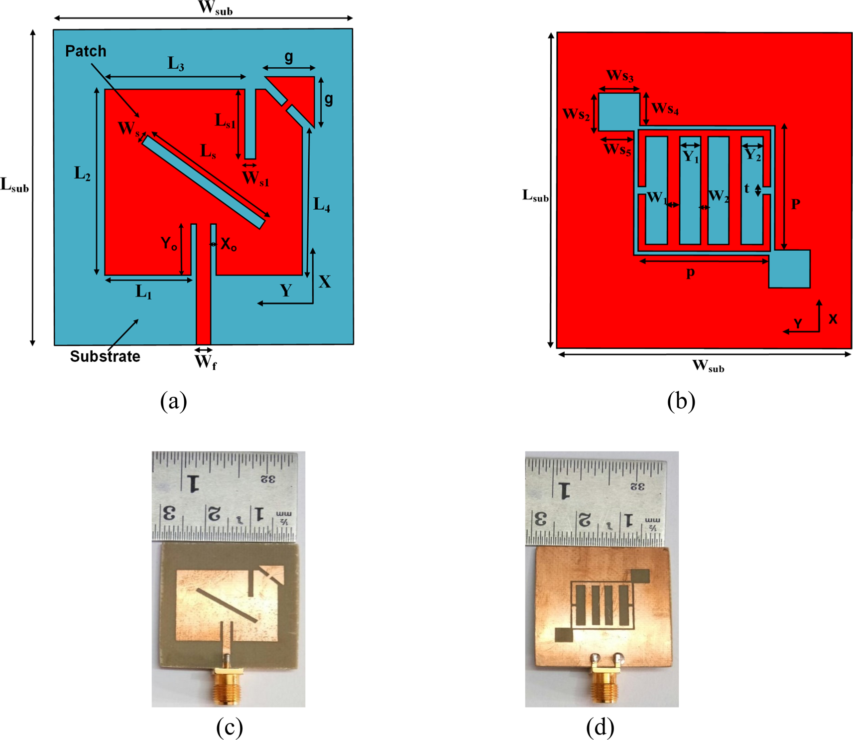
Fig. 1. Layout of the prospective CP antenna: (a) front view, (b) back view, (c) front view of the prototype, (d) back view of the prototype.
Table 1. Prospective antenna design parameters.

Modified electric−inductive−capacitive (m-ELC) resonator
The physical parameters of the proposed m-ELC resonator are shown in Fig. 1(b). To analyze its operating behavior, the m-ELC resonator unit cell is simulated with a 50-Ω transmission line. The orientation and boundary conditions of the m-ELC unit cell are illustrated in Fig. 2. Figure 3 exhibits the reflection and transmission coefficients of the presented m-ELC.

Fig. 2. Simulation set-up of an m-ELC resonator.

Fig. 3. Simulated outcomes of the prospective m-ELC (a) magnitude, (b) phase.
In the simulation set-up, the feeding points are positioned along the Y-axis while the periodic boundaries (perfect electric conductor and perfect magnetic conductor) are positioned in the Z- and X-axes, respectively. A microstrip line is placed orthogonal to the feeding ports, and the input signal propagates from port-1 to port-2. The microstrip line responds to in-plane magnetic fields while the m-ELC resonator responds to orthogonal electric fields. Since m-ELC is working as a single negative metamaterial, the stop bands occur at 1.95 and 4.25 GHz, as illustrated in Fig. 3.
Furthermore, the prospective m-ELC resonator is studied with the help of circuit theory. In the past, various SRR/CSRR designs with 50-Ω microstrip line loading were investigated by many researchers [Reference Schurig, Mock and Smith26–Reference Gil, Bonache, Gil, Garcia, Martin and Marques28]. The equivalent circuit of the prospective m-ELC is depicted in Fig. 4. Here, the m-ELC resonator is modeled as a parallel tank circuit while the microstrip line is modeled as an inductance Ltl. The coupling between the microstrip line and the parallel tank circuit is modeled as Cc. CELC 1 represents the capacitance of two outer rings, while LELC 1 and LELC 2 represent the inductance of outer and inner finger loops, respectively.

Fig. 4. Equivalent circuit of the proposed m-ELC.
In the literature, several techniques have been reported to extract material parameters of the unit cell [Reference Smith, Schultz, Markos and Soukoulis29–Reference Chen, Lei, Yang, Shi and Zhang33]. The parameters (ɛ and μ) of the proposed m-ELC are computed using Nicolson−Ross−Weir (NRW) method. Complex S11, S12, S21, and S22 are used for computing (ɛ m−ELC and μ m−ELC) parameters. The refractive index (nm −ELC) of m-ELC is calculated using the following bianisotropic medium formula [Reference Li, Aydin and Ozbay32].

It is evident that if S 11 = S 22, then Eq. (1) will be the same standard retrieval equation given in [Reference Smith, Schultz, Markos and Soukoulis29]. During the computation of nm −ELC, Eq. (1) has many possible solutions as discussed in references [Reference Smith, Schultz, Markos and Soukoulis29, Reference Chen, Grzegorczyk, Wu, Pacheco and Kong31]. For passive medium

In comparison to the isotropic medium, the bianisotropic medium has different characteristic impedance in different propagation directions (±y in the presented case).


For a passive medium, the impedances $z_{m-ELC}^ +$ and $z_{m-ELC}^-$
 must follow the given criteria

where ξ 0 is the magneto-electric coupling coefficient, k is the free space wave number, and d m−ELC is the largest dimension of the m-ELC unit cell.
The fundamental resonant frequency of an m-ELC is calculated as

where LELC and CELC represent the total inductance and capacitance of the m-ELC, respectively. The parameters of the proposed m-ELC are plotted in Fig. 5, which shows negative metamaterial behavior at two resonant bands.

Fig. 5. Material parameters (ɛm−ELC and μ m−ELC) of the prospective m-ELC.
Development of the prospective antenna
The development stages of the prospective CP multiband antenna are demonstrated in Fig. 6. As shown in Fig. 6(a), the design process starts with Antenna-1, which is an inset-fed rectangular microstrip patch antenna operating at 3.35 GHz. The radiator size of the antenna-1 is 22 × 20 mm2. The antenna is modified by introducing a wide slot and a rectangular slot (rotated by 55°) in the ground plane and the resonating patch, respectively, as demonstrated in Fig. 6(b). Antenna-2 exhibits dual-band linearly polarized attributes. As displayed in Fig. 6(c), the antenna-3 is realized by loading an m-ELC unit cell in the wide slot of the antenna-2.

Fig. 6. Design steps of the prospective antenna.
In step 4, two square-shaped slots are etched from the ground of the antenna-3 as portrayed in Fig. 6(d). The square-shaped slots introduce a quadrature-phase difference between the two current vectors and also improve the impedance matching. Further, the rectangular patch is truncated and an arrow-shaped stub is introduced at the corner of the radiator to induce circular polarization (antenna-5) as illustrated in Fig. 6(e). In Fig. 6(f), a slit is cut along the top edge of the radiator for better impedance matching in the two upper bands. The return loss and axial ratio variations of the design steps are demonstrated in Figs 7(a) and 7(b), respectively.

Fig. 7. Response of the design stages (a) S11, (b) axial ratio.
Parametric study of the prospective antenna
The parametric study of the prospective multiband CP antenna is demonstrated in Figs 8–11. The parametric analysis is divided into four stages. In stage 1, the effect of the ground plane slots (Ws 2, Ws 3) is studied. The values of Ws 2 and Ws 3 are varied and their effect on the axial ratio is observed. It is clear from Fig. 8 that Ws 2 affects the 3.8 GHz band significantly whereas a small influence is seen on the other bands. A similar effect is seen in the case of Ws 3.

Fig. 8. Effect of Ws 2 on axial ratio.

Fig. 9. Effect of slit parameters on axial ratio (a) Ws 1, (b) Ls 1, (c) Ys.

Fig. 10. Effect of arrow dimension (g) on axial ratio.

Fig. 11. Effect of diagonal slot parameters on axial ratio (a) Ls, (b) Ws.
In stage 2, the effect of slit dimensions (Ls 1, Ws 1, Ys) is presented in Fig. 9. The slit dimensions are optimized to shift 3-dB axial ratio bands at 3.18 and 3.82 GHz. The optimized dimensions of the slit are selected as Ws 1 = 1.2 mm, Ls 1 = 7.5 mm, and Ys = 4.6 mm. In stage 3, the length (g) of the arrow-shaped patch is varied and its effect on the axial ratio band is presented. It is depicted in Fig. 10 that g influences the 3.18 GHz band significantly, and its value is chosen as 5.5 mm.
In stage 4, the effect of rectangular slot (Ls, Ws) is presented. It is depicted in Fig. 11 that Ls and Ws affect the 2.78 GHz band considerably, and their dimensions are chosen as 16 and 1.1 mm, respectively.
Results and analyses
The prospective antenna physical size is 0.26λ 0 × 0.22λ 0, and the radiator size is 0.16λ 0 × 0.14λ 0, where free-space wavelength (λ 0) is calculated at the first resonant frequency. In comparison to conventional antenna design, the loaded m-ELC saves space of ~62%. The quad-band resonances are obtained due to the slotted patch and m-ELC resonator. The etched slit/slot shifts resonant frequency towards the lower side, thus decreasing the size of the antenna [Reference Zachou, Mayridis, Christodoulou and Chryssomallis25]. The CP bands are obtained by means of the truncated corner, arrow-shaped stub, and square-shaped slots etched from the antenna ground.
The surface current circulation at 2.2, 2.78, 3.18 and 3.82 GHz is demonstrated in Fig. 12. It can be noticed in Fig. 12(a) that (at 2.2 GHz) the current concentration is high around the fingers of m-ELC. Whereas, at 2.78 GHz, the current concentration is high across the rectangular slot of the patch and wide slot of the ground, as demonstrated in Fig. 12(b). At 3.18 GHz, the current concentration is high around the square-shaped slots of the ground and slit of the patch as shown in Fig. 12(c). While, at 3.82 GHz, the current concentration is high around the periphery of the m-ELC resonator as displayed in Fig. 12(d).

Fig. 12. Surface current circulation at different resonance frequencies (a) 2.2 GHz, (b) 2.78 GHz, (c) 3.18 GHz, (d) 3.82 GHz.
For obtaining circular polarization, the two electric field components (Ex and Ey) must have an equal magnitude (|Ex| = |Ey|) and quadrature-phase difference (±90°) between them. To get a better understanding of the polarization, the current vectors are examined at 2.78, 3.18 and 3.82 GHz. It is demonstrated in Fig. 13(a) that magnitude of the electric field components (in X-direction (Ex) and Y-direction (Ey)) is almost equal at 2.78, 3.18 and 3.82 GHz. The phase variation of two electric field components is illustrated in Fig. 13(b), which clearly illustrates that phase difference between the two fields is 90°.

Fig. 13. Variations of Ex and Ey (a) magnitude, (b) phase.
To check the sense of polarization, the surface current vectors are plotted at 2.78, 3.18 and 3.82 GHz. It is clear from Fig. 14(a) that the resultant current vector rotates in a clockwise direction, which illustrates left-hand circularly polarized (LHCP) operation at 2.78 GHz. Similarly, at 3.18 GHz, the resultant current vector rotates in a clockwise direction, thus illustrating LHCP operation of the antenna, shown in Fig. 14(b). While, at 3.82 GHz, the resultant current vector rotates in a counter-clockwise direction, thus illustrating right-hand circularly polarized (RHCP) operation of the antenna as illustrated in Fig. 14(b).

Fig. 14. Surface current circulation at (a) 2.78 GHz, (b) 3.18 GHz, (c) 3.82 GHz.
The experimental testing of the fabricated prototype is done using the Agilent N5230A PNA-L series vector network analyzer. Comparative outcomes of simulated and experimental return loss are displayed in Fig. 15(a). The experimental −10 dB bandwidth is 80 MHz (3.58%) at 2.23 GHz, 75 MHz (2.64%) at 2.84 GHz, 80 MHz (2.50%) at 3.19 GHz, and 70 MHz (1.82%) at 3.83 GHz. The simulated impedance bandwidth is 90 MHz (4.09%) at 2.2 GHz, 70 MHz (2.51%) at 2.78 GHz, 100 MHz (3.14%) at 3.18 GHz, and 50 MHz (1.30%) at 3.82 GHz. The comparison between the simulated and measured axial ratio is illustrated in Fig. 15(b). The experimental 3-dB axial ratio bandwidths (in the +Z-direction) are 40 MHz (1.41%), 100 MHz (3.12%), and 60 MHz (1.57%) at 2.84, 3.20 and 3.82 GHz, respectively. Whereas, the simulated 3-dB axial ratio bandwidths are 60 MHz (2.15%), 80 MHz (2.51%), and 40 MHz (1.05%) at 2.78, 3.18 and 3.82 GHz. A small mismatch is seen between the simulated and experimental outcomes, which may be due to the fabrication and measurement errors. The comparison between simulated and measured gain is demonstrated in Fig. 16.

Fig. 15. Simulated and experimental outcomes (a) S11, (b) axial ratio.

Fig. 16. Gain of the prospective antenna.
The radiation pattern measurements are conducted in a reverberation chamber with the help of an Agilent signal analyser (HP 8563E) and Anritsu (MG3694B) microwave signal generator. A standard horn antenna is used as a transmitter and the proposed antenna as a receiver. The physical separation (200 cm) between the transmitting and receiving antenna is fixed to satisfy the far-field conditions. The simulated and experimental patterns in E-(Y-Z) and H-(X-Z) planes are demonstrated in Fig. 17. It can be noticed in Fig. 17(a) that (at 2.2 GHz) bidirectional pattern is obtained in the E-plane, while in the H-plane, the pattern is omnidirectional. The antenna shows LHCP behavior (at 2.78 GHz and 3.18 GHz) in the E- and H-planes and RHCP behavior at 3.82 GHz as illustrated in Figs 17(b), 17(c), and 17(d).

Fig. 17. Simulated and experimental patterns of the prospective antenna at (a) 2.2 GHz, (b) 2.78 GHz, (c) 3.18 GHz, (d) 3.82 GHz.
A comparative study of the prospective design and other published CP multiband designs is conferred in Table 2. Most of the published multiband designs consisted of two/three layers, therefore, the alignment of multiple layers is an issue. The antenna reported in [Reference Wang, Zhu, Guo and Wu8] consisted of four vias, therefore, it could be difficult to integrate on the PCB. In contrast to the previously published CP designs, the prospective design is low-profile, compact, and it does not need any external phase shifter or complex feed mechanism for introducing circular polarization. A low gain is realized, which is due to the modified ground plane of the antenna.
Table 2. Comparison of the prospective antenna with published multiband antennas.

Conclusion
In this study, a compact low-profile quad-band antenna is suggested with three CP bands. The prospective inset-fed antenna comprised of a rectangular radiator and a modified ground surface. The multiband operation is achieved by loading an m-ELC resonator in the antenna ground and engraving a rectangular slot on the patch. The CP operation is achieved by truncating a corner of the patch and introducing an arrow-shaped stub in it. One more CP band is obtained by etching the opposite edges of the wide slot by means of two square-shaped slots. The prospective antenna is fabricated and measurement outcomes demonstrate a close affinity with the simulated results. The antenna operational frequency bands are 2.23, 2.84, 3.19, and 3.83 GHz. The prospective design is easy to manufacture, offers reasonable gain, and CP radiation at three bands. The antenna can be used for space to earth communication (2.17–2.2 GHz), airport surveillance radar/aviation services (typically operate in the 2.7–2.9 GHz range), Wi-MAX (3.3 GHz), and unmanned aerial vehicle (UAV)/Wi-MAX (3.8 GHz) applications.
 Ghanshyam Singh received the B.Tech. degree in electronics and communication engineering from Uttar Pradesh Technical University, Lucknow, India, in 2004, and the M.E. degree in electronics and communication engineering from the National Institute of Technical Teachers Training and Research, Chandigarh, India, in 2013. In 2007, he joined the Department of Electronics and Communication Engineering, Feroze Gandhi Institute of Engineering and Technology, Raebareli, India, as a lecturer. He also worked as an electronics engineer in the Railway Testing Division of M/s Central Electronics Limited, India. Currently, he is working towards his Ph.D. degree in electronics engineering from Dr. A.P.J. Kalam Technical University, Lucknow, India. His research interests include patch antennas, artificial electromagnetic materials, and reconfigurable MIMO antennas.
 Binod Kumar Kanaujia received the B.Tech. degree in electronics engineering from Kamla Nehru Institute of Technology, Sultanpur, India, in 1994, and the M.Tech. and Ph.D. degrees from the Department of Electronics Engineering, Indian Institute of Technology Banaras Hindu University, Varanasi, India, in 1998 and 2004, respectively. He is currently a professor with the School of Computational & Integrative Sciences, Jawaharlal Nehru University, New Delhi, India. He has been credited to publish more than 350 research articles with more than 2900 citations and h-index of 25 in several peer-reviewed journals and conferences. He had supervised 50 M.Tech. and 15 Ph.D. scholars in the field of RF and microwave engineering. He is currently on the editorial board of several international journals. He is also a member of several academic and professional bodies, such as the Institution of Engineers, India, the Indian Society for Technical Education, and the Institute of Electronics and Telecommunication Engineers of India. He had successfully executed five research projects sponsored by several agencies of the Government of India, such as DRDO, DST, AICTE, and ISRO.
 Vijay Kumar Pandey received the B.E. degree in electronics engineering from the University of Poona, India, in 1990, and the M.E. degree in control and instrumentation from the University of Delhi, India, in 1997. He received the Ph.D. degree in electronics engineering from the Indian Institute of Technology Banaras Hindu University, Varanasi, India, in 2006. Currently, he is working as a professor in the Department of Electronics and Communication Engineering, Noida Institute of Engineering & Technology, Greater Noida, India. He received a grant of Rs. 14.5 lakhs under MODROB scheme from the All India Council for Technical Education, New Delhi, India, for establishing a project/research laboratory. His research interests include CP antennas, reconfigurable antennas, metamaterial-inspired antennas, and microwave components.
 Sachin Kumar received the B.Tech. degree in electronics and communication engineering from Uttar Pradesh Technical University, Lucknow, India, in 2009, and the M.Tech. and Ph.D. degrees in electronics and communication engineering from Guru Gobind Singh Indraprastha University, Delhi, India, in 2011 and 2016, respectively. He is currently a researcher with the School of Electronics Engineering, Kyungpook National University, Daegu, South Korea. His current research interests include circularly-polarized antennas, reconfigurable antennas, ultra-wideband antennas, defected ground structure, and microwave components.


