I. INTRODUCTION
The use of ultra-wideband (UWB) communications systems operating over 3.1–10.6 GHz is proliferating widely as it enables high-speed communications at data rates of gigabits per second over short distances. This technology allows multiple devices to interact with each other seamlessly over a wireless medium. Miniaturization of such systems demands the use of highly compact bandpass filters (BPF) with high selectivity [1–Reference Zhang, Xiao, Tang and Guo4]. In addition, such systems require notched-band filters to suppress undesired interference from communications systems that coexist in the UWB frequency spectrum, in particular WiMAX (3.4–3.6 GHz), wireless local area network (WLAN) (5.15–5.35 and 5.725–5.825 GHz), radio-frequency identification (RFID) (6.7–6.9 GHz), X-band satellite communication services (downlink: 7.25–7.75 GHz, uplink: 7.9–8.395 GHz) [Reference Borhani, Honarvar and Virdee5–Reference Guo14]. In an attempt to meet some of these requirements, in [Reference Shang2] multi-mode resonator (MMR) technique is used to develop an UWB filter in combination with stepped-impedance stub (SIS). This device lacks in notched-band response to eliminate interference signals and its upper stop band is relatively narrow. In [Reference Borhani, Honarvar and Virdee5], high selectivity UWB filter is achieved by using asymmetrical coupled lines to reject the WLAN band. In [Reference Song and Xue6], asymmetric coupling lines are used to generate dual notched-band; however, its upper stopband is very narrow for practical applications. Another high selectivity filter with dual notched-bands is reported in [Reference Sarkar, Ghatak, Pal and Poddar7], and a triple notched-band in [Reference Wang, Zhao and Li8, Reference Shi, Xi, Zhao and Yang9]. Unfortunately, the rejection skirts and circuit size of these devices are prohibitively poor. Recently, a triple notch UWB filter was reported in [Reference Kumar, Gupta and Parihar10] that has excellent skirt factor at 3.6, 5.2, and 8.4 GHz; however once again its circuit size is relatively large and it has a narrow upper stopband. Until now there has been little work in literature on designing quad notched-band UWB BPFs other than in [Reference Dong, Sun, Fu and Shao12–Reference Guo14]. In [Reference Dong, Sun, Fu and Shao12], a stub-loaded MMR is used to realize an UWB filter where two folded L-shaped shunt open-circuited stubs are located in the feed-lines to introduce notched-bands. The resulting device is however relatively large. The technique in [Reference Nosrati and Daneshmand13] is based on combining tri-section stepped-impedance resonators (SIR) and incorporating a gap-coupled resonator to realize multiple notched-bands in the passband of the UWB filter. Quad notched-band generated in [Reference Guo14] is achieved with eight arrow-shaped resonators. The selectivity of this device is poor.
The above overview shows the challenge of designing UWB BPFs that are highly compact and possess characteristics of high selectivity, quad notched-band functionality, and wide stopband. To address the limitations of the previously reported UWB BPFs, in this paper we propose a novel filter that meets these requirements. The desired passband (3.1–10.6 GHz) is obtained by using MMR technique with asymmetric interdigital coupled feed-lines and coupled parasitic element to generate multiple resonate modes in the desired frequency range and two transmission zeroes at 2.77 and 10.89 GHz that greatly enhances the filter's selectivity. In the proposed technique the notched-bands can be controlled by simply modifying the structure's dimensions.
II. QUAD-NOTCHED-BAND UWB BPF
A) Proposed MMR features
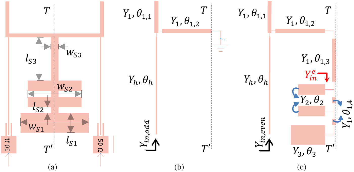
Figure 1 shows the basic structure of the proposed MMR and its odd- and even-mode equivalent circuits. MMR is weakly coupled to input/output 50 Ω feed-lines. The dotted line T – T′ indicates the MMR's symmetric plane. The MMR structure is composed of two modified SIS, whereby one SIS is a U-shaped low-impedance transmission line with two tapped high-impedance lines. This structure is responsible for producing three resonant modes. The length of high-impedance lines and the low-impedance line are λ g /4 and λ g /2, respectively, where λ g is guided-wavelength with respect to center frequency. The U-shaped SIS is directly coupled to another SIS structure, which is composed of an open-circuited transmission line loaded with three low-impedance lines, two of them having the same characteristic impedance. This SIS structure provides a greater degree of freedom to tune three even resonant modes one of which is used to extend the upper stopband. From the resonance conditions, i.e. Y in,odd = 0 andY in,even = 0, the resonant frequencies for odd and even modes can be determined as follows:
 $$Y_1 - Y_1{\rm tan}\theta _{1,1}{\rm tan}\theta _{1,2} - Y_h{\rm tan}\theta _h{\rm tan}\theta _{1,2} = 0,$$
 $$\eqalign{& Y_1(Y_{in}^e + jY_1{\rm tan}(\theta _{1,2} + \theta _{1,3})) + j(Y_1{\rm tan}\theta _{1,1} \cr & \quad + Y_h{\rm tan}\theta _h)(Y_1 + jY_{in}^e {\rm tan}(\theta _{1,2} + \theta _{1,3})) = 0,} $$
where
 $$Y_{in}^e = \displaystyle{\matrix{Y_1^2 (jY_3{\rm tan}\theta _3 + jY_1{\rm tan}\theta _{1,4}) + jY_1(Y_2{\rm tan}\theta _2 \hfill \cr + Y_1{\rm tan}\theta _{1,4})(Y_1 - Y_3{\rm tan}\theta _3{\rm tan}\theta _{1,4}) \hfill} \over \matrix{(Y_1^2 - Y_1Y_3{\rm tan}\theta _3{\rm tan}\theta _{1,4}) \hfill \cr - (Y_1Y_3{\rm tan}\theta _3 + Y_1^2 {\rm tan}\theta _{1,4}) \hfill \cr+ jY_2{\rm tan}\theta _2{\rm tan}\theta _{1,4}(Y_1 - Y_3{\rm tan}\theta _3{\rm tan}\theta _{1,4})\; \hfill}} + jY_2{\rm tan}\theta _2.$$
When Y in,odd = Y in,even , the transmission zeros can be determined.

Fig. 1. (a) Basic structure of the proposed MMR structure, (b) odd-mode equivalent circuit, and (c) even-mode equivalent circuit.
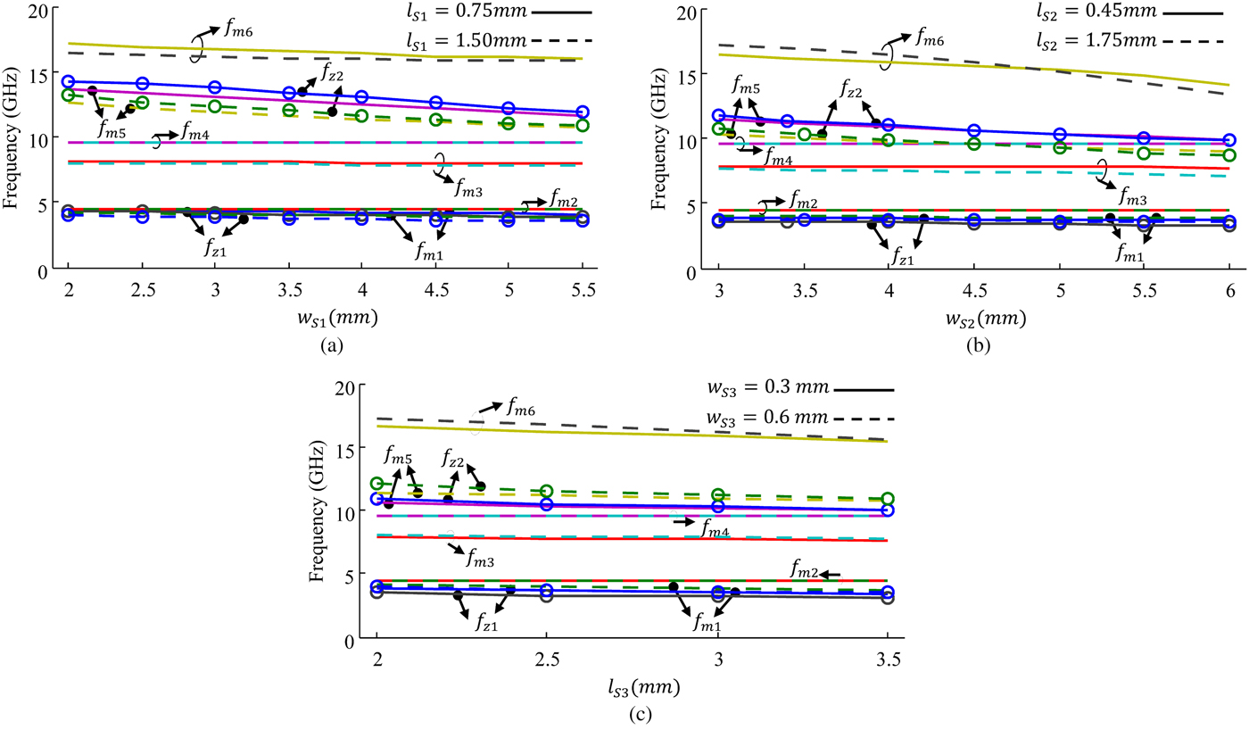
Parametric analysis of the modified SIS configuration using electromagnetic simulator ADS, is shown in Fig 2. The behavior of six resonant modes (f m1, f m2, f m3, f m4, f m5, f m6) and two transmission zeros (f z1, f z2) was investigated to suitably locate five resonant modes to realize the required UWB passband, and the two transmission zeros were located at the filter's cutoff frequency to increase its selectivity performance. The sixth mode is used to extend the upper stopband of the filter. Based on (2), resonate modes (f m5, f m6) and zero (f z2) can be adjusted by varying wide w S1 from 2 to 5.5 mm for l S1 = 0.75 and l S1 = 1.50 mm; in fact, f m1, f m6, f z2 go down in frequency with increase in w S1, however there is a marginal increase in f m4. For l S2 = 0.45 and l S2 = 1.75 mm the resonant modes f m5 and f m6 decrease in frequency as w S2 increases from 3 to 6 mm; however, the converse marginally applies to f m4, as shown in Fig. 2(b). It is evident in Fig. 2(c) by increasing l S3 from 2 to 3.5 mm also cause f m6 and f z2 to decrease in frequency for w S2 of 3 and 6 mm.

Fig. 2. Effect by the MMR parameters on the frequency locations of its poles and zeros, (a) l S1, w S1, (b) l S2, w S2, and (c) l S3, w S3 (these parameters are shown in Fig. 1).
It was found there is a trade-off between selectivity and wider upper stopband by adding extra low-impedance stubs to the SIS structure. In Figs 3(a) and 3(b), the proposed MMR structure in Fig. 1 is shown with slight variation in its configuration. The first five resonant modes of the two structures are located, as shown in Fig. 3(c), in the same location to produce a single passband, however the sixth resonant mode in MMR#2 provides a wider stopband than MMR#1. In fact, the sixth resonant mode in MMR#2 is about 1.61 GHz higher up in frequencies than MMR#1 though with slight effect on its upper selectivity. Compared with the SIS structure in [Reference Shang2], the proposed SIS configuration provides greater degree of freedom to adjust the sixth resonant mode in order to extend the upper stopband than is the case in [Reference Shang2].
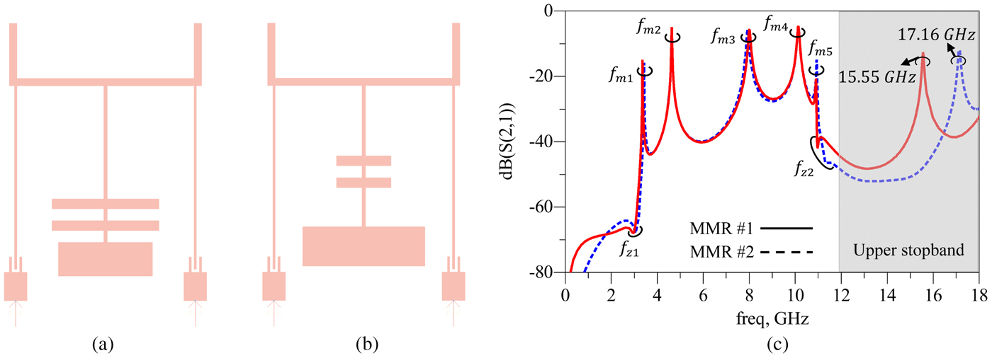
Fig. 3. (a) MMR#1, parameters: l S1 = 1.33, w S1 = 3.68, l S2 = 0.45, w S2 = 4.18, w S3 = 0.15, l S3 = 4.41, and (b) MMR#2, parameters: l S1 = 1.55, w S1 = 4.78, l S2 = 2.14, w S2 = 4.18, w S3 = 0.15, l S3 = 2.74, (c) comparison of |S 21| of MMR#1 and MMR#2 (dimensions in millimeters).
B) Quad-notched-band implementation
To implementation of rejection bands within the passband of the proposed UWB were investigated using the proposed MMR configuration. The two variations of the MMR structure are shown in Fig. 4. The microstrip lines contributing towards the formation of the notched-bands are depicted in red color, which do not in any way have an impact on the footprint of the proposed MMR configuration. Microstrip lines coupled to each feed-line produce dual narrow notched-bands; hence, the combined effect results in an UWB BPF with quad notched-band. In Fig. 4(a), the proposed MMR structure is coupled to the feed-lines with two dissimilar asymmetric interdigital coupling. In one case the inner coupled line is folded. Its effects are primarily determined by parameters L A1 and W A1. In the other feed-line the inner coupled line is not folded however the outer line is shortened. In this case its features are governed by parameters L A2 and d A2. The asymmetric interdigital coupling lines produce a well defined UWB passband with high selectivity with quad notched-band that can be controlled by changing the structural parameters (L A1, W A1, L A2, d A2). In Fig. 4(b), the U-section in the MMR configuration is coupled to a parasitic element formed by embedding a uniform λ g /2 low-impedance line with two folded λ g /2 high-impedance open-circuited tapped lines. The parasitic element also creates two additional notched-bands in the passband of the UWB filter. The parasitic coupled element can be modeled in term of an LC circuit.

Fig. 4. (a) MMR structure with different asymmetric feed-line coupling, and (b) MMR structure with symmetric feed-line coupling and a parasitic element.
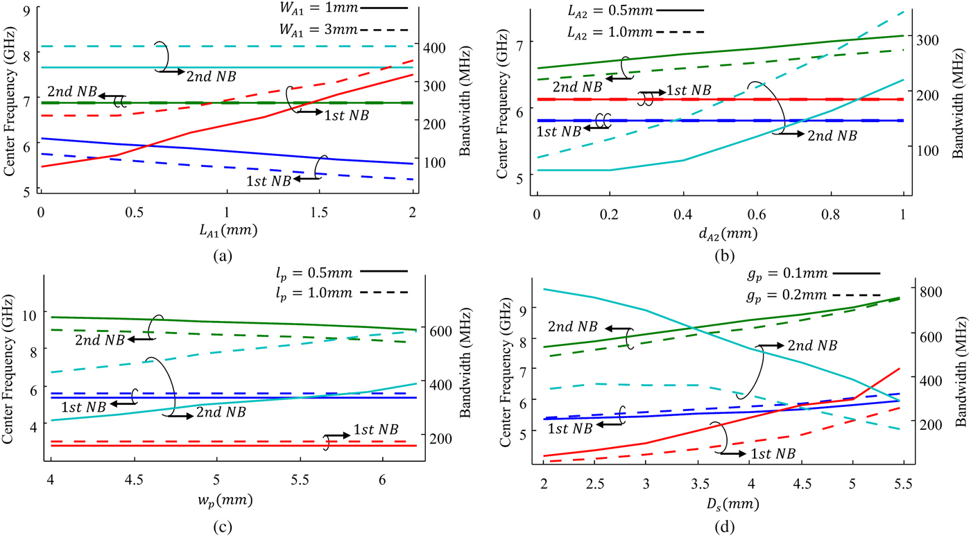
As it can be seen in Fig. 5(a) center frequency of first notch decreased from 6.1 to 5.54 GHz and its bandwidth (BW) increased from 80 to 320 MHz as length L A1 is increased, while the second notched-band remains unchanged at 6.88 GHz with a constant BW of 340 MHz. W A1 could be used to provide wider BW for both notches. The second notched-band can be independently tuned by adjusting L A2 and d A2, as indicated in Fig. 5(b). When d A2 is increased, the second notched-band and its BW increases from 6.6 to 7.1 GHz and from 54 to 220 MHz, respectively. To achieve a wider BW with this notched-band, L A2 can be increased. Effect of coupled parasitic element is shown in Figs 5(c) and 5(d). The width of low-impedance section, i.e. w p , varies the center frequency of the second notched-band from 9.72 to 9 GHz, and its bandwidth from 250 to 388 MHz; however the first notched-band remains fixed at a center frequency of 5.38 GHz and bandwidth of 154 MHz. Length of low-impedance section, l p , can be used to determine the 3 dB-BW of second notched-band, and this parameter can also shift the first notched-band up in frequency. Figure 5(d) shows the center frequencies of the two notched-bands that can be moved from 5.34 to 5.95 GHz and from 7.7 to 9.32 GHz, respectively, by increasing the distance between two tapped high-impedance lines, D s . In this case the BW of first notched-band increases greatly from 40 to 439 MHz, however BW of second notch decreases significantly from 793 to 293 MHz. The results show when gap between parasitic coupled element and U-section of the MMR becomes greater, BW of both notched-bands becomes narrower. Therefore the required quad notched-bands can be achieved with a high degree of freedom for each center frequency and their 3-dB BWs can be adjusted to exactly reject unwanted signals from UWB system.

Fig. 5. Center frequency and bandwidth of the notched bands (NBs) as a function of: (a) L A1, W A1, (b) L A2, d A2, (c) l p , wp , and (d) D s , gp implementation in the configuration in Fig. 4.
III. FINAL DISCUSSION AND MEASUREMENT RESULTS
The finalized configuration of the proposed quintuple-mode UWB filter with quad notched-band is shown in Fig. 6. Optimized dimensions of the proposed structure in Figs 1, 4, and 6 are: w u = 0.3, L u1 = 6.9, L u2 = 2.45, l S1 = 1.32, w S1 = 4.79, l S2 = 0.45, w S2 = 3.92, w SL = 0.4, l S3 = 4.11, w S3 = 0.15, w p = 6.01, l pa = 1.38, l p = 0.62, D p = 4.08, g p = 0.1, L pu = 2.62, L A1 = 0.54, W A1 = 1.9, l A1 = 0.64, L A2 = 0.95, d A2 = 0.78, L SG = 6.88, W SG = 1, W 0 = 0.9 (all dimensions are given in millimeters). All other strip widths and gap widths are 0.1 mm.
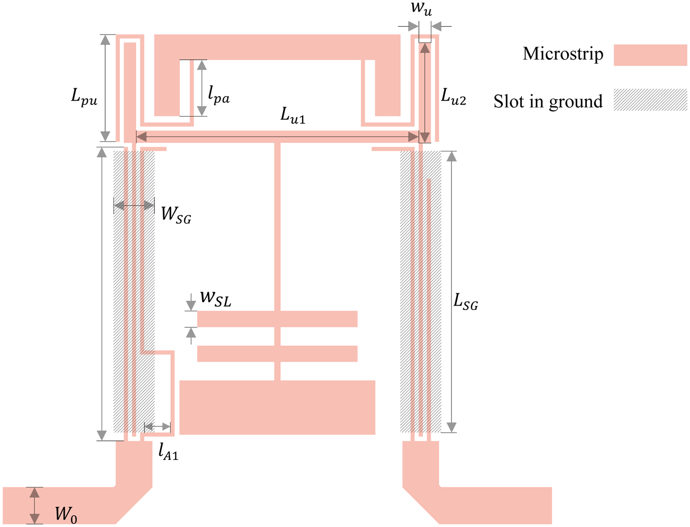
Fig. 6. Final structure of the proposed quad notched-band UWB BPF.
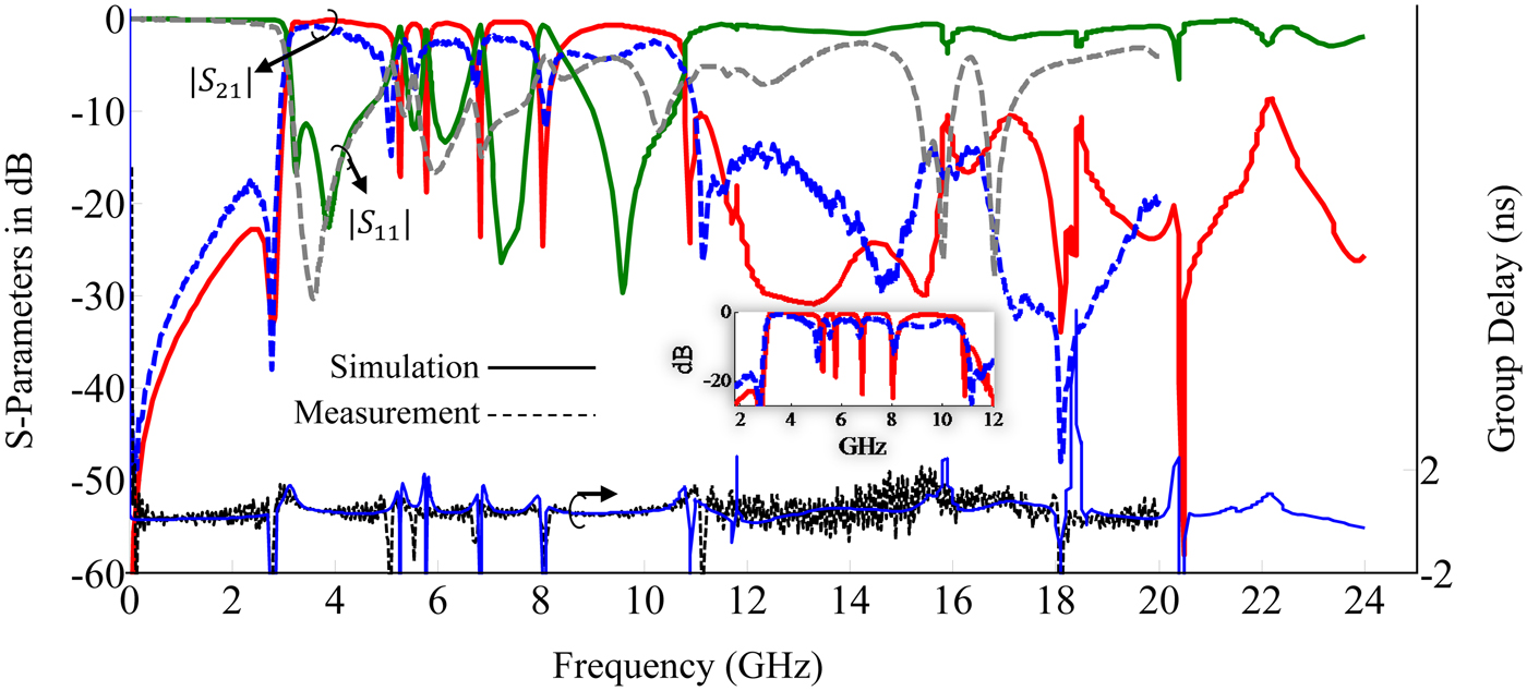
Slots in the ground plane are used to improve the in-band performance of the filter. The UWB BPF was verified through fabrication and measurement using Agilent 8510C network analyzer. Figure 7 shows the photograph of the fabricated quad notched-band UWB BPF. Comparison between simulation and measured results is plotted in Fig. 8, which shows generally good agreement. The discrepancy between the two results is mainly attributed to manufacturing tolerance, imperfect soldering of the SMA connectors, and to a lesser extend variation in the material parameters. There is good agreement in the simulation and measured response in the lower frequency range. It was found that by enclosing the filter in a metallic housing had marginal effect on the filter's performance especially at higher frequencies, which is attributed to box modes.
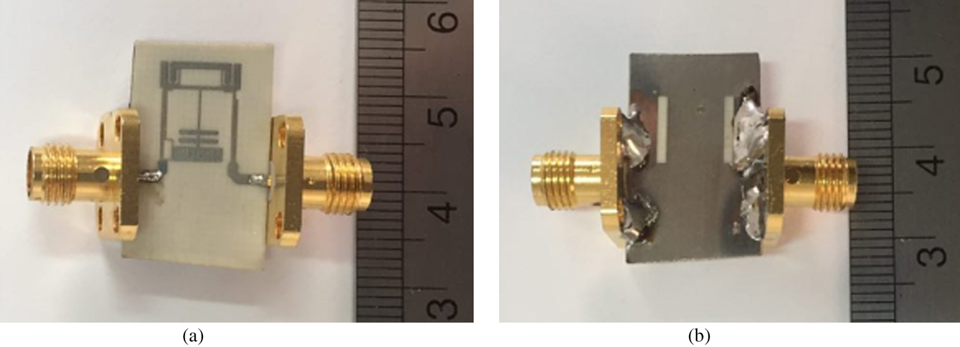
Fig. 7. Fabricated filter, (a) top view, and (b) bottom view.

Fig. 8. Simulated and measured S-parameters of the proposed UWB filter.
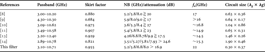
The results show the two transmission zeros at 2.76 and 11.14 GHz create an UWB BPF with enhanced frequency selectivity. The proposed BPF satisfies the FCC regulation for UWB systems from 3.1 to 10.6 GHz with skirt factor (3–20 dB BW) of 0.955, a tremendously high value. The measured passband is from 3.09 to 10.45 GHz with a return loss better than 11.37 dB. Rejection level over the lower frequencies is greater than 20 dB resulting from locating the sixth resonant mode to cancel out the transmission zeros of the coupled lines. The upper rejection is greater than 10 dB extends up to 22 GHz, which is a very wide upper stopband. Measurement results show notched-band with center frequencies of 5.08, 5.56, 6.73, and 8.1 GHz. Hence, the proposed quad narrow notched-band with rejection notched-band greater than 16.9 dB effectively suppresses interference signals of 5.2 (WLAN), 5.8 (WLAN), 6.8 (RFID), and 8.15 (X-band). The measured group delay of the filter, shown in Fig. 8, varies between 0.1 and 1.47 ns over regions excluding the notched-band. The proposed structure is highly compact with a size of 8.0 × 9.83 mm2. Table 1 shows a comparison of the proposed UWB BPF with other notched-band UWB filters.
Table 1. Comparison with other UWB BPFs with multiple notched-bands.

NB: Center frequencies of notched-bands. f u : upper stopband with 10 dB rejection level.
IV. CONCLUSION
A highly compact microstrip quintuple-mode UWB BPF is designed for high selectivity, quad notched-band in the passband, and a very wide upper stopband performance. The filter comprises a MMR that generates six resonant modes and two transmission zeros. Feed-lines to the filter use asymmetrical interdigital coupled lines to create notched-band whose center frequencies can be controlled by modifying the dimensions of the coupled lines. Additional notched-bands are created by incorporating a parasitic coupled element. The notched-bands are centered at 5.2, 5.8, 6.8, and 8 GHz to reject interference signals from WLAN, RFID, and X-band satellite communication system, respectively. Good agreement is observed between the simulation and the measurement results. Measured results confirm the performance of the proposed UWB filter that exhibits sharp rejection skirts and quad notched-band in its passband.
 Seyyed Jamal Borhani was born in Shiraz, Iran, in 1986. He received B.Sc. and M.Sc. degrees in Communication Engineering from Najafabad Branch Islamic Azad University, Isfahan, Iran, in 2010 and 2013, respectively. His research interests include RF and microwave device design and fabrication. He has authored some papers in scientific journals. He is currently an academic lecturer in Electrical Engineering.
 Mohammad Amin Honarvar was born in Shiraz, Iran in 1982. He received M.Sc. degree in Telecommunication Engineering from Shiraz University, Shiraz, Iran, in 2008, and Ph.D. degree from Science and Research branch, Islamic Azad University, Tehran, Iran, in 2012. Since 2012 he has been with Department of Electrical Engineering, Najafabad Branch, Islamic Azad University, Isfahan, Iran, as an Assistant Professor. His research interests include numerical methods in electromagnetics and microwave circuit and components design.
 Bal S. Virdee received the B.Sc. (Hons.) and M.Phil. degree in Communications Engineering from the University of Leeds, Leeds, UK, and the Ph.D. degree in Electronic Engineering from the University of London, London, UK. He has worked in industry for various companies, including Philips (U.K.) as an R&D engineer and Filtronic Components Ltd. as a future products developer in the area of RF/microwave communications. Previously he was a lecturer at several institutions. He is a Professor of Microwave Communications in the Faculty of Life Sciences and Computing at London Metropolitan University, where he Heads the Center for Communications Technology and is the Director of London Metropolitan Microwaves. His research, in collaboration with industry and academia, is in the area of microwave wireless communications encompassing mobile phones to satellite technology. Professor Virdee has chaired technical sessions at IEEE international conferences and published numerous research papers. He is a Fellow of IET.