I. INTRODUCTION
Recent digital modulation techniques associated with multiplexing techniques provide high information transmission capacity, high data security, and fast system availability in modern communications. Consequently, radio frequency (RF) or microwave power transistors characterization must be performed under conditions that are similar to those used in operating modes. Envelop varying signals present an increased peak to average power ratio, which requires a drastic trade-off between power-added efficiency (PAE) and linearity. In this paper, we present an original experimental characterization setup, operating in the 1.5–2.5 GHz frequency band and specially devoted to device linearity optimization. To our knowledge, it is the first time that a measurement system using wideband-modulated signals simultaneously and independently provides
– fundamental and harmonic frequency (f 0 and 2f 0) source-pull/load-pull characterization,
– low frequency impedances optimization, and
– base-band predistortion linearization technique.
Generally, fundamental frequency load-pull and source-pull measurements provide optimum impedances for output power (or PAE) and input matching, respectively. On the other hand, distortions in power transistors are largely influenced by the source impedance at the fundamental frequency [Reference Liu, Dunleavy and Arslan1–Reference Marchetti, Pelk, Buisman, Neo, Spirito and de Vreede4]. Consequently, if the input is matched for best gain and input return loss, the device does not operate at its best linear performance. Source-pull measurements presented in this paper are performed in order to find a trade-off between power gain and linearity. Unfortunately, applying source-pull/load-pull techniques at f 0 does not provide the required linearity for modern communication systems. Moreover, it has been shown that the harmonic load and source impedances [Reference Spirito, Pelk, Van Rijs, Theeuwen, Hartskeerl and de Vreede5, Reference Colantonio, Giannini, Limiti and Teappati6] and low-frequency-memory effects, mainly due to the envelope impedance of the bias networks [Reference Williams, Leckey and Tasker7–Reference Bensmida, Bergeault, Abib and Huyart10], have a strong impact on linearity performances. Therefore, distortions in power transistors can also be reduced by independent control of the harmonic and base-band impedances. Finally, a significant improvement in linearity can be achieved using instantaneous memoryless base-band predistortion obtained by reversing the amplitude to amplitude conversion (AM/AM) and amplitude to phase conversion (AM/PM) characteristics [Reference Muhonen, Kavehrad and Krishnamoorthy11, Reference Abib, Bensmida, Bergeault and Huyart12]. The results concerning the load/source-pull at f 0, the low-frequency impedances optimization, and the base-band predistortion have been presented in [Reference Abib, Bergeault, Bensmida and Huyart13]. The new results in comparison to [Reference Abib, Bergeault, Bensmida and Huyart13] concern the load/source-pull optimization at 2f 0. A complete description of this measurement system is presented in Section II, and experimental results obtained on an MESFET power device at 1.575 GHz biased in class-AB are reported in Section III.
II. MEASUREMENT SYSTEM DESCRIPTION
Figure 1 shows the simplified structure of the measurement system. The device under test (DUT) is biased with bias tees BT1 and BT2 (0.8–4 GHz) and DC supply.

Fig. 1. Power transistor characterization system.
A) Variation of load and source impedances at f 0 and 2f 0
Variation of the fundamental or harmonic frequency impedance can be carried out passively by means of a tuner or actively by injecting a power wave toward the transistor [Reference Deshours, Bergeault, Jallet and Huyart14–Reference Ferrero and Pisani17]. In the proposed setup, source-pull/load-pull measurements at fundamental and harmonic frequencies are performed using an active loop architecture. Thus, the setup is composed of four active loops: two at the source side (at f 0 and 2f 0) and two at the load side (at f 0 and 2f 0). Source impedances at f 0 and 2f 0 are controlled independently by means of the broadband circulator Cir1 and the band-pass filters BPF1 and BPF2. The same configuration is used at the DUT output termination with the circulator Cir2 associated with the band-pass filters BPF3 and BPF4. Each active loop is associated with a six-port reflectometer used as an automatic network analyzer that allows the measurement of the reflection coefficient of the source impedances ΓS(f 0) and ΓS(2f 0) (by six-ports 1 and 4, respectively) [Reference Bergeault, Gibrat, Bensmida and Huyart18], the reflection coefficient of the load impedances ΓL(f 0) and ΓL(2f 0) (by six-ports 2 and 3, respectively), and finally the DUT input reflection coefficient Γin(f 0) (by six-port 1). This solution is attractive as very low-cost six-port reflectometers can be implemented in microstrip technology. An active loop (which is detailed in Fig. 1 and used for fundamental source impedance control) includes a high-gain power amplifier A 2, a phase shifter, and a variable attenuator. Consequently, high values for the magnitude of the source reflection coefficient can be synthesized at the DUT plan. A reconfigurable yttrium iron garnet (YIG) filter is used to avoid loop oscillations and is set to be centered at the loop frequency of operation. Depending on the position of the switch SW1, the six-port reflectometers 1 and 4 measure either the input reflection coefficients of the DUT Γin(f 0) and Γin(2f 0) (SW1 in position 2) or the reflection coefficient presented to its input ΓS(f 0) and ΓS(2f 0) (SW1 in position 1). A simple one-step calibration procedure is required as the calibration constants of the six-port reflectometer are independent of SW1 position.
B) Low-frequency impedances optimization
Low-frequency load impedances Z LLF are synthesized at the signal envelop frequency (equal to 1 MHz for the measurement results reported in this paper) using an electronically controlled passive tuner realized with resistors, capacitors, and inductors. In order to achieve independent control of RF and low-frequency impedances, two different bias tees are combined at the output of the DUT: high-frequency bias tee BT2 (0.8–4 GHz) associated with low-frequency bias tee BT4 (10 kHz–12 GHz). Similarly, the low-frequency source impedance Z SLF can also affect transistor linearity. Consequently, the same configuration is used for base-band impedance control at the DUT input. The electrical delay of these terminations must be minimized to avoid variation of the reflection coefficient within the bandwidth of the modulated signal. The total phase shift of the base-band reflection coefficient is about 8°/MHz. The bandwidth of the test signal is actually limited to 5 MHz but a wider bandwidth can be achieved with six-port diode detectors showing lower values of the video resistance [Reference Abou Chakra and Huyart19].
C) Base-band predistortion linearization technique
An instantaneous memoryless polynomial base-band predistortion is deduced from the measurements of AM/PM and AM/AM characteristics. The complete description of the base-band predistortion method is reported in [Reference Abib, Bensmida, Bergeault and Huyart12]. AM/PM conversion is measured by a digital oscilloscope, whereas instantaneous AM/AM conversion is obtained by means of two fast zero-bias Schottky diodes D 1 and D 2 followed by a data acquisition card. Diode detectors operate only in the square law region at low power levels. In order to achieve accurate measurements over a wide power dynamic range, a linearization procedure of the diodes is applied according to the method described in [Reference Bergeault, Huyart, Geneves and Jallet20]. Adjacent channel power ratio (ACPR) and error vector magnitude (EVM) measurements are performed using a spectrum/signal analyzer connected at the output of the DUT. The original and corrected base-band signals are stored in the arbitrary waveform generator of the RF vector signal generator. The different steps for the calibration of the measurement system are the following:
• Calibration of the six-port reflectometers (measurement of power levels Pin and Pout, reflection coefficients of the DUT, and source/load reflection coefficients) using the method described in [Reference Bensmida, Bergeault, Abib and Huyart10].
• Linearization of the fast zero-bias Schottky diodes [Reference Bergeault, Huyart, Geneves and Jallet20] (measurement of AM/AM).
III. EXPERIMENTAL RESULTS
The measured power device is a GaAs MESFET (Fujitsu FLL107ME) biased in class-AB (V GSQ = −1.7 V, VDSQ = 10 V, and I DSQ = 44 mA). The QPSK-modulated signal, centered at 1.575 GHz with a 1-MSps symbol rate, is provided by the RF source with an input power level equal to 10 dBm corresponding to the 1-dB compression point.
A) Source-pull/load-pull measurements at f 0 and 2f 0
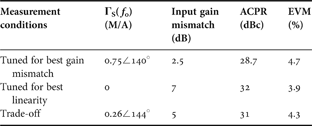
Initial values for fundamental and harmonic source and load impedances are equal to 50 Ω. The first optimization concerns the determination of the fundamental load impedance that optimizes Pout (f 0) and PAE. The optimum load reflection coefficient ΓL(f 0) = 0.4∠128°, obtained from load-pull measurements, increases output power from 26 to 28 dBm. At the same time, PAE is increased from 37 to 53%. Then a complete source-pull characterization is performed at f 0. Both ACPR and EVM are measured as well as gain mismatch at the input, i.e. when ΓS = Γin*. Depending on the value of the source reflection coefficient, variations of 3 dB, 5 dB, 1 percentage point, and 10 dB are observed for ACPR, ACPR asymmetry, EVM, and input gain mismatch, respectively. The conjugate matched source impedance is in the instable zone and could lead to oscillations of the transistor. Consequently, in this region, the magnitude of the source reflection coefficient is limited to 0.8. Figure 2(a) shows the locations of the optimum source impedances obtained for gain mismatch and linearity. Moreover, source-pull contours for gain mismatch are also plotted. Figure 2(b) shows the fundamental source-pull contours for ACPR. The measurement results show that the fundamental source impedance ZS(f 0) has a significant effect on linearity. Linearity is degraded when the source impedance varies from 50 Ω (optimum linearity) to a conjugate match (optimum input gain mismatch). These observations are in agreement with those reported in [Reference Liu, Dunleavy and Arslan1] on an L-band high-power GaAs FET device. Consequently, a trade-off between input gain mismatch and linearity has to be found. For a source reflection coefficient ΓS(f 0) = 0.26∠144°, ACPR and EVM are close to their optimum values (Table 1). On the other hand, this trade-off impedance decreases the optimum stable mismatch gain by 3 dB but, compared to the worst case, improves ACPR and EVM by 2.3 dB and 0.4 point, respectively.

Fig. 2. Source-pull contours at f 0 for (a) gain mismatch and (b) ACPR.
Table 1. Effects of source impedance at f 0.

For the load-pull measurements at 2f 0, no optimal impedances for output power, PAE, and linearity at the same time were found. Thus, we decided to set |ΓL(2f 0)| to 0.9 and the phase φ of ΓL(2f 0) was swept from 0 to 360°. Figures 3(a) and 3(b) show ACPR, Pout(f 0), and EVM, PAE versus φ(ΓL(2f 0)), respectively. We notice that Z L(2f 0) has an important influence on ACPR and EVM, leading to variations equal to 9 dB and 3 points, respectively. Unfortunately, when linearity increases, Pout and PAE decrease and vice versa. Therefore, Z L(2f 0) is chosen to be set to 50 Ω. The same measurement procedure was performed with the source impedance at 2f 0. |ΓS(2f 0)| was set to 0.9 and the phase φ of ΓS(2f 0) was swept from 0 to 360°. Figures 4(a) and 4(b) show ACPR, Pout(f 0), and EVM, PAE versus φ(ΓS(2f 0)), respectively. As observed previously, when linearity increases (4 dB variations for ACPR), Pout and PAE decrease and vice versa. Unlike the load impedance, the source impedance at the second harmonic improves the linearity when φ(ΓS(2f 0)) = 270°. This impedance, compared to the worst and 50 Ω cases, improves the ACPR by 3 and 1.5 dB, respectively, whereas the output power and efficiency are maintained at their optimal values (Pout = 28 dBm and PAE = 52%). We have also retuned the load-pull at f 0 after optimizing the second harmonic load. For this transistor, the optimum load at the fundamental frequency remains unchanged. Of course, this would not be the case depending on the DUT. All these results show the usefulness of the harmonic source and load-pull characterizations. If there are no optimal impedances, at least performance degradation can be avoided.

Fig. 3. (A) ACPR and Pout versus φ, and (B) EVM and PAE versus φ when |ΓL(2f 0)| = 0.9 and φ(ΓL(2f 0)) is variable.

Fig. 4. (A) ACPR and Pout versus φ, and (B) EVM and PAE versus φ when |ΓS(2f 0)| = 0.9 and φ(ΓS(2f 0)) is variable.
B) Low-frequency impedances optimization
The load and source reflection coefficients at the fundamental frequency are now fixed to 0.4∠128° and 0.26∠144°, respectively. At 2f 0, ΓL(2f 0) = 0 and ΓS(2f 0) = 0.9∠270°. Figures 5(a) and 5(b) show the large influence of low-frequency load impedances Z LLF on transistor linearity (ACPR and EVM versus Pout, respectively) over a wide output power range. As expected, the optimum impedance is close to a short circuit while an open circuit significantly reduces the device linearity. However, it is important to measure the influence of Z LLF because compensation of electrical, thermal, and trap effects can lead to an optimum complex value [Reference Sevic, Burger and Steer8, Reference Bensmida, Bergeault, Abib and Huyart10]. Depending on the base-band impedance, maximum ACPR and EVM variations are found to be 15 dB and 5.5 points, respectively. One observes maximum ACPR close to the compression point for an output power equal to 26 dBm due to the gain expansion phenomena. Therefore, the control of this impedance presents a significant potential advantage since the highest linearity can be achieved at a substantially improved efficiency and output power (Pout = 28 dBm, PAE = 52%, ACPR and EVM improvements equal to 10 dB and 5.5 points, respectively). On the other hand, no significant influence of low-frequency source impedances Z SLF has been observed for this transistor, but this would not be the case for strongly non-linear transistors like HBT for example [Reference Williams, Leckey and Tasker7].

Fig. 5. (A) ACPR versus Pout, and (B) EVM versus Pout for different low-frequency load impedances Z LLF.
C) Base-band predistortion linearization technique
Fundamental and low-frequency terminations are fixed to previously determined values. Transistor linearity can still be improved by applying instantaneous memoryless base-band predistortion using the same setup. Figures 6(a) and 6(b) show the ACPR and EVM values versus Pout, with and without predistortion. The linearization procedure does not have a significant effect in the linear region. Otherwise, in the compression region, improvements of 5 dB and 1 percentage point are observed for ACPR and EVM, respectively. Predistortion can be applied up to a limit value equal to 28.5 dBm corresponding to the saturation of transistor for which the memoryless linearization procedure is no longer efficient.

Fig. 6. (A) ACPR versus Pout, and (B) EVM versus Pout with and without linearization.
IV. CONCLUSIONS
An original measurement system including active multi-harmonic and low-frequency source-pull/load-pull techniques and instantaneous memoryless base-band predistortion has been presented. This setup is mainly devoted to the design of high-linearity and high-efficiency power amplifiers. Measurements performed at 1.575 GHz on a power MESFET biased in class-AB, and operating under a QPSK signal, illustrate features of the measurement system. In the compression zone and compared to worst-case values, ACPR and EVM can be approximately improved by 20.3 dB and 6.5 points, respectively, while maintaining high output power and high PAE. Consequently, knowledge of the effects of all the input/output terminations at base-band, fundamental, and harmonic frequencies associated with a base-band linearization procedure will help to design a high power amplifier with very high linearity and efficiency.
 Ghalid Idir Abib was born in Algiers, Algeria, in 1977. He received the Engineer degree and a Master (Magister) degree in electronics from the Université des Sciences et de la Technologie Houari Boumediene (USTHB), Algiers, Algeria, in 1999 and 2002, respectively, the Diplome d'Etudes Approfondies (DEA) degree from the Ecole Nationale Supérieure des Télécommunications (ENST), Paris, France, in 2003, and a Ph.D. degree in electronics and communications from the Université Pierre et Marie Curie (UPMC) Paris 6, Paris, France, in 2007. He is currently working as temporary assistant professor at the Université Pierre et Marie Curie, France. His research involves power transistor characterization and linearization and transimpedance amplifier design.
 Eric Bergeault (M'00) was born in Limoges, France, in 1963. He received the Diplôme d'Etudes Approfondies (DEA) degree from the University of Limoges, Limoges, France, in 1987, and a Ph.D. degree in electronics and communications from the Ecole Nationale Supérieure des Télécommunications (ENST), Paris, France, in 1991. In 1998, he earned the accreditation to supervise research from the University of Limoges. From 1987 to 1990, he was a research engineer with the Laboratoire Central des Industries Elecriques (LCIE), Fontenay aux Roses, France. In 1991, he joined ENST, where he is currently a full professor. His research interest is in the field of microwave instrumentation. He is mainly involved with network analyzers, characterization of nonlinear devices, and modelization and applications to the optimization of power amplifiers.
 Souheil Bensmida received the DEA degree in electronics and instrumentation from the University of Pierre and Marie Curie Paris 6, Paris, France, in 2000, and a Ph.D. degree in electronics and communications from the Ecole Nationale Supérieure des Télécommunications (ENST), Paris, France, in 2005. From October 2006, he has been a Post-Doctoral Fellow with the iRadio Laboratory, University of Calgary, Calgary, AB, Canada. He is now a research associate at University of Bristol, UK. His research interest is in the non-linear characterization and linearization of power amplifiers for mobile and satellite applications and microwave instrumentation.
 Reda Mohellebi was born in Algiers, Algeria, in 1984. He received the Engineer degree in electronics from the Ecole Nationale Polytechnique (ENP), Algiers, Algeria, in 2007 and a Master degree from the Université Pierre et Marie Curie (UPMC), Paris, France, in 2008 and is currently working toward a Ph.D. degree at Telecom ParisTech (ENST), Paris, France. His research involves power transistor characterization in the millimeter-wave band.