


Introduction
Polarization and band reconfigurable antennas have drawn significant attention due to their applications in cognitive radios and smart communication systems [Reference Bernhard1]. By using a polarization reconfigurable antenna, an multipath fading effect can be handled easily, and the system capacity can be improved [Reference Bernhard1]. Such reconfigurable antennas are suitable for radars, microwave sensing, tracking, and direction finding [Reference Saraswat and Harish2].
Several antenna designs have been proposed by researchers to achieve polarization reconfigurability or band reconfigurability [Reference Bernhard1]. Various techniques are used to alter the current path within the antenna by integrating RF switches to achieve reconfigurability e.g. by placing the RF switching element within the feed network, radiating element, or in the ground plane [Reference Saraswat and Harish2,Reference Saraswat and Harish3].
Conventionally, cross-slot antennas are used to produce single band circular polarization [Reference Wong4]. In recent past, several cross-slot antennas are proposed for the polarization reconfigurability and frequency reconfigurability by embedding switching elements within the cross slot [Reference Chen, Sun and Feng5–Reference Dhar, Patra, Ghatak, Gupta and Poddar12]. These antennas can be divided into two categories: (i) the switchable cross is embedded within the radiating element and (ii) the switchable slot is embedded in the ground plane. In [Reference Chen, Sun and Feng5], two switchable slots in the ground plane form a cross which is excited by a microstrip line and in [Reference Lin and Wong6], a square patch is excited by a switchable cross slot to achieve ± 45° polarization reconfigurability.
A coaxial probe fed nearly square patch antenna consisting of a switchable asymmetric cross slot is placed with an offset for the polarization reconfigurability [Reference Yang and Rahmat-Samii7]. The nearly square patch excites two degenerate modes, TM01 and TM10, which are altered by the RF switching element, resulting in the switchable polarization from right-hand circular polarization (RHCP) to left-hand circular polarization (LHCP) and vice-versa. Similarly, for the polarization reconfigurability, edge fed square patch [Reference Monti, Corchia and Tarricone8], and a rectangular patch excited by a microstrip line [Reference Boti, Dussopt and Laheurte9] consisting of switchable cross-shaped slots are used. In [Reference Hyun, Baik, Lee and Kim10], RF switching elements are embedded within a symmetric cross slot, which is inserted in the radiating coaxial probe fed microstrip patch for achieving reconfigurability.
Recently, in [Reference Ge, Li, Wang and Sim11], 48 p–i–n diodes are embedded in a cross-shaped slot which is etched on the substrate integrated waveguide cavity for band and polarization reconfigurability. The switchable cross-slot aperture is used to excite a dielectric resonator antenna for the polarization reconfigurability in [Reference Dhar, Patra, Ghatak, Gupta and Poddar12]. All these presented antennas [Reference Chen, Sun and Feng5–Reference Dhar, Patra, Ghatak, Gupta and Poddar12] are narrow band single resonating structures and none of the antennas demonstratea multi-band response.
This paper describes a polarization and band reconfigurable cross-slot antenna for multiband application. The proposed antenna consists of four p–i–n diodes which are integrated within the cross slot to create un-equal arm lengths. By switching the state of the p–i–n- diodes, it is possible to reconfigure the state of polarization and the frequency band of the proposed structure. The proposed antenna can produce two linearly polarized (LP) bands or one circularly polarized (CP) band and two LP bands. The sense of rotation can be reconfigured from LHCP to RHCP or vice-versa.
The organization of the paper is as follows. In the section “Antenna configuration”, the antenna configuration along with a description of the techniques used to generate circular polarization and reconfigurability is presented. The details of the fabricated prototype of the proposed antenna along with the measured and simulated results are given in the section “Experimental results and discussion”.
Antenna configuration
The physical geometry of the proposed antenna is illustrated in Fig. 1 (top and bottom views). The proposed antenna is fabricated on a low cost FR-4 substrate having permittivity εr = 4.3, loss tangent tan δ = 0.025, anda substrate height of 1.56 mm. In the proposed antenna, a crossed shaped slot is etched from the ground plane. Two arms of the grounded slot are equal in size, length L s, and width g s. The crossed slot is coupled with the cross-shaped shaped microstrip feed line of width W f and length L f. Two microstrip stubs (Stub-1 and Stub-2) are placed at a distance of L s1 and L s2 from the feed point.
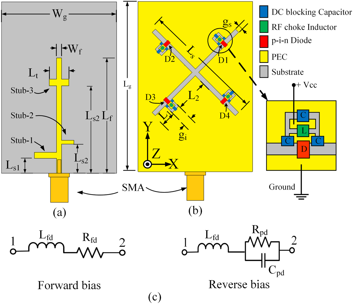
Fig. 1. Proposed antenna structure (inset biasing arrangement): (a) front side, (b) back side, and (c) p–i–n diode equivalent circuit (where p–i–n diode, D = BAP70-02, DC blocking capacitor, C = 22 nF, RF choke inductor, L = 39 nH, L fd = 1.5 nH, C pd = 0.1 pF, R pd = 5 KΩ, and R fd = 1.5 Ω).
Since asymmetric arm length of the crossed slot excited by the microstrip line can generate circular polarization [Reference Sievenpiper, Hsu and Riley13], four RF switching elements are embedded within the crossed-slot arm to realize asymmetric arm lengths. By switching alternate p–i–n diodes, alternate arms of the cross slot can be made asymmetric. This results in a change in the sense of the CP wave. In the current study, BAP70-02 p–i–n diode (NXP semiconductor) is used as the RF switching element. The equivalent circuit of different biasing states of the p–i–n diodes used in the full wave EM simulation is shown in Fig. 1. As shown in Fig. 1, the RF choke (L) is used for RF blocking and for biasing the p–i–n diode and connected through a metallic island (used for the electrical connection to the DC supply, V cc). To avoid the DC short and to provide high-frequency continuity to the p–i–n diode, a DC blocking capacitor (shown in Fig. 1 as C) is used.
A commercially available EM simulator is used to optimize the antenna utilizing iterative methods. The optimized dimensions of the proposed antenna are as follows: L g = 52 mm, W g = 35 mm, L s = 36 mm, L 1 = 4.32 mm, L 2 = 10.23 mm, g i = 2.75 mm, g s = 1.4 mm, W f = 1.5 mm, L t = 6 mm, L s1 = 4.5 mm, L s2 = 8.8 mm, L s3 = 26.5 mm, and L f = 35.01 mm.
Based on the parametric variation of structure dimensions, it is observed that the lower band (Band-1) and upper band (Band-3) can be tuned by varying the slot width and length. The CP band (Band-2) is controlled by the location of the switch and for a given pair of the cross-slot dimension, narrow range of CP band can be achieved.
Generation of circular polarization
A cross slot can be represented as two orthogonal slots. By asymmetric arm length of the cross slot, phase offset corresponding to each orthogonal slot is created and with proper slot length tuning, 90° phase difference can be achieved in the far-field [Reference Dhar, Patra, Ghatak, Gupta and Poddar12]. This results in the circular polarization. The switching elements (p–i–n diode) are symmetrically placed close to the opposite ends of the arms. The p–i–n didoes are located at a distance of L 2 from the center. For each pair of “ON” state of the p–i–n diode, by tuning L 2, two orthogonal field modes can be produced having equal amplitude and 90° phase difference.
The simulated electric field distribution is observed at 20 mm from the antenna surface at 3.2 GHz at different time instances. As shown in Fig. 2 the dominant electric field is rotating in the clockwise direction for ωt = 0° to ωt = 270° for State-4, which results in the generation of left-hand circular polarization.

Fig. 2. Simulated electric field distribution at 3.2 GHz for different time instances (State-4).
Polarization and band reconfigurability
In the proposed antenna, four diodes (namely D1, D2, D3, and D4) are used to achieve polarization and band reconfigurability. Using four diodes, 16 possible states can be realized. Due to similar binary patterns and similar antenna performances for the different states, only unique solutions are considered. Hence, for brevity only six states are presented and shown in Fig. 3. All diodes are switched “OFF” to realize State-1 and turned “ON” for State-2, respectively. This results in longer arm length for State-1 and shorter arm length for State-2, respectively. By switching “ON” either D1 and D3 or D2 and D4, two asymmetric arm lengths are created, which results in circular polarization for State-3 and State-4, respectively. Similarly, by switching “ON” either D1 and D2 or D3 and D4, State-5 and State-6 can be achieved. Different states obtained by diode biasing and the corresponding responses are summarized in Table 3.
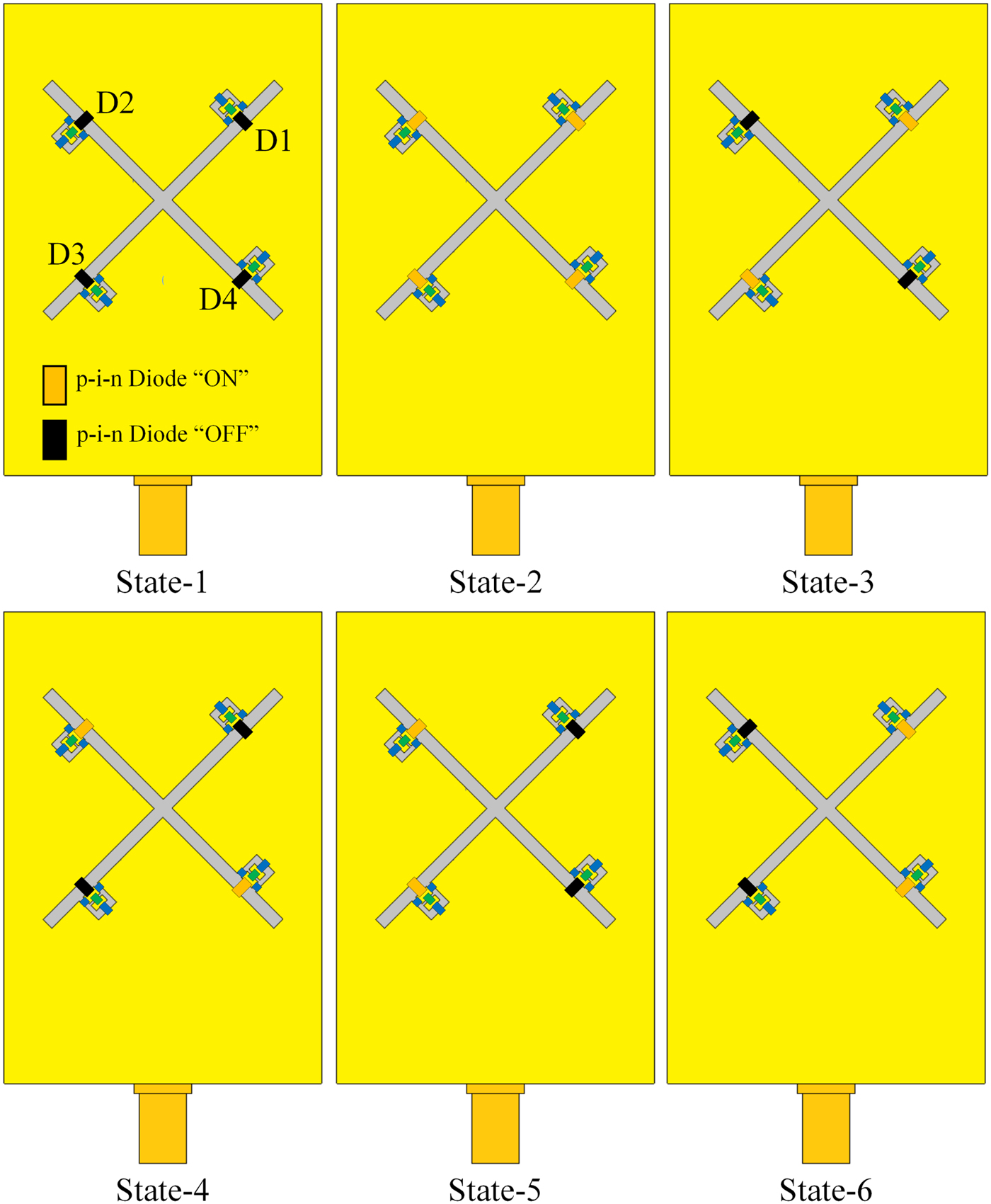
Fig. 3. The p–i–n diode biasing condition for different states.
Effect of p–i–n diode loading on antenna performance
Within the slot, the p–i–n diode acts as a shunt switch and therefore, the p–i–n diode affects the input impedance characteristics as well as the radiation characteristics of the antenna. The discrete elements, Lf and Cp shown in Fig. 1(c) affect the input impedance and the resonant frequency of the antenna. The effect of Lf and Cp can be compensated by varying the slot width (g s) and length (L s). Ohmic loss is observed, when the p–i–n diode is inthe “ON” state, due to forward resistance R f of the p–i–n diode. This ohmic loss not only affects the input impedance of the antenna but also the radiation characteristics. For example, Table 1 summarizes the effect of the forward resistance (R f) on the antenna efficiency. The efficiency is only 60% with R f = 0. This is due to the ohmic losses in other non-ideal devices.
Table 1. Effect of forward resistance on antenna efficiency

Experimental results and discussion
The proposed single-feed dual-polarized crossed-shaped antenna is fabricated and tested. The photograph of the proposed antenna is shown in Fig. 4(a). Thebiasing network and biasing elements are shown in Fig. 4(a) (inset). The antenna performance is measured usingan Agilent PNA-L Network Analyzer N5230A. Figure 4(b) illustrates the experimental setup for the reflection coefficient measurement. The bias line of the proposed antenna is connected to an in-house developed controller board (using PIC 18F4550 microcontroller). The I/O pins of the controller board are used to activate/deactivate the p–i–n diodes. A laptop connected to the controller board through a USB is used to set the states of the p–i–n diodes. The complex horizontal and vertical far-field components, E H and E V, respectively, are measured inside an anechoic chamber using a standard LP horn antenna. The LHCP and RHCP radiation patterns can be obtained by combining E H and E V field components as follows [Reference Toh, Cahill and Fusco14]:
 $$ E_{RHCP}= {{1} \over {\sqrt{2}}} \left(E_H + jE_V\right) $$
 $$ E_{LHCP}= {{1} \over {\sqrt{2}}} \left(E_H - jE_V\right) $$
Fig. 4. Proposed antenna: (a) top view ofthe fabricated antenna (inset: each biasing network consisting of three capacitors, inductor, p–i–n diode, and DC bias line) and (b) experimental setup.
The axial ratio is measured using the ‘rotating source’ method [15], where a LP antenna is mounted on a rotator and the maximum E max and minimum E min field values are recorded by rotating this antenna. The axial ratio is given as,
 $$ AR({\rm dB})=20{\rm log} \left( {{\vert E_{max}\vert} \over {\vert E_{min}\vert}}\right) $$
Figure 5 presents the simulated and measured input reflection coefficient and axial ratio of the proposed antenna for different states. Figure 5(a) shows the input reflection coefficient of the antenna for State-1 and State-2. Similarly, for State-3 and State-4, reflection coefficient is shown in Fig. 5(b) and axial ratio is shown in Fig. 5(d). Figure 5(c) depicts the simulated and measured reflection coefficient for State-5 and State-6.

Fig. 5. Measured and simulated parameters: (a) reflection coefficient for State-1 and State-2, (b) reflection coefficient for State-3 and State-4, (c) reflection coefficient for State-5 and State-6, and (d) axial ratio for State-3 and State-4.
From these figures the bandwidths and the band edge frequencies for various bands corresponding to different states were computed and are summarized in Table 3. In the bands corresponding to the lowest and the highest frequencies (Band-1 and Band-3, respectively) the antenna is LP. By changing the state of operation, it is possible to tune the operating frequency of bands 1 and 3.
Table 2. Summary of measured and simulated results

(S): simulation results and (M): measurement results.
Table 3. Comparison of reconfigurable cross-slot antennas

In States 3 and 4, the antenna operates as a triple band antenna, with the antenna radiating LP waves in the upper and lower bands (Bands 1 and 3, respectively) and CP waves in the middle band (Band-2). By switching the states from 3 to 4, the state of polarization changes from right hand circular polarization to left hand circular polarization. The measured and simulated axial ratio bandwidths corresponding to AR<3 dB are 7.2% (3.17–3.407 GHz) and 10.85% (3.05–3.4 GHz), respectively.
The frequencies corresponding to the band edges and also the bandwidths were computed from the measured data and are listed in Table 3. A good agreement between the measured and simulated results can be seen in the table. Some differences in the simulated and measured results are due to the fabrication tolerances.
Figures 6–12 show the measured and simulated normalized radiation patterns of the proposed antenna operating in different states in both XZ- and Y Z-planes. For State-1, Figs 6 and 7 show the measured and simulated normalized radiation patterns at 2.3 GHz (Band-1) and 4.8 GHz (Band-2) in XZ- and Y Z-planes, respectively. Similarly, the simulated and measured radiation patterns at 2.9 GHz (Band-1) and 5.0 GHz (Band-2) in both the planes when the antenna is operating in State-2 are shown in Figs 8 and 9.

Fig. 6. Measured and simulated radiation pattern for State-1 (linearly polarized) in xz XZ- and yz YZ-planes at 2.3 GHz (Band-1).

Fig. 7. Measured and simulated radiation pattern for State-1 (linearly polarized) in xz XZ- and yz YZ-planes at 4.8 GHz (Band-2).

Fig. 8. Measured and simulated radiation pattern for State-2 (linearly polarized) in xz XZ- and yz YZ-planes at 2.9 GHz (Band-1).

Fig. 9. Measured and simulated radiation pattern for State-2 (linearly polarized) in xz XZ- and yz YZ-planes at 5.0 GHz (Band-2).

Fig. 10. Measured and simulated radiation pattern for State-3 (linearly polarized) in xz XZ- and yz YZ-planes at 2.33 GHz (Band-1).
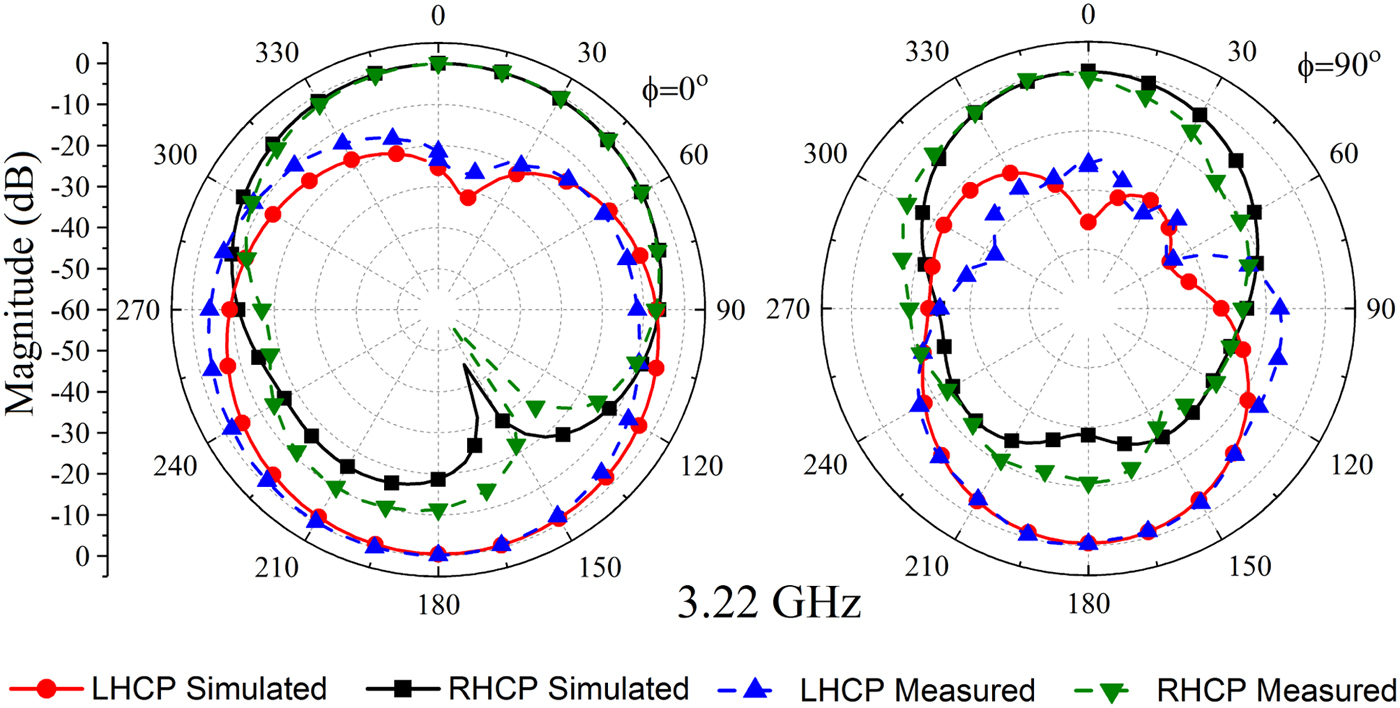
Fig. 11. Measured and simulated radiation pattern for State-3 (circularly polarized) in xz XZ- and yz YZ-planes at 3.22 GHz (Band-2).

Fig. 12. Measured and simulated radiation pattern for State-3 (linearly polarized) in xz XZ- and yz YZ-planes at 4.97 GHz (Band-3).
Figure 10 shows the normalized radiation patterns for State-3 at 2.33 GHz (Band-1) in XZ- and Y Z-planes. For State-3, the proposed antenna produces right hand circular polarization in Z>0 half space when operating in Band-2. The normalized simulated and measured radiation patterns are shown in Fig. 11 in the XZ- and Y Z- planes at 3.22 GHz (Band-2) which is corresponding to circular polarization. Similarly, Fig. 12 shows the simulated and measured normalized radiation patterns at 4.97 GHz (Band-3). The measured radiation patterns agree well with the simulated radiation patterns. A high cross polar level is observed in the LP radiation pattern in Band-1 and Band-3, which is a characteristic of the cross-slot antenna [Reference Sievenpiper, Hsu and Riley13].
A comparison of the proposed antenna with other reported cross-slot reconfigurable antennas highlights the main advantage of the proposed structure. Table 3 compares the performance of different types of cross-shaped antennas with the proposed structure. The antennas proposed in [Reference Chen, Sun and Feng5–Reference Dhar, Patra, Ghatak, Gupta and Poddar12] are narrow single-band antennas. In [Reference Chen, Sun and Feng5,Reference Lin and Wong6], the ± 45° polarization reconfigurability is achieved. In [Reference Yang and Rahmat-Samii7–Reference Hyun, Baik, Lee and Kim10,Reference Dhar, Patra, Ghatak, Gupta and Poddar12], sense of the CP wave is reconfigured. In [Reference Ge, Li, Wang and Sim11], the polarization and frequency reconfigurability is achieved, but the antenna consists of 48 p–i–n diodes as switching elements. The axial ratio of the proposed antenna is wider than the antennas discussed in [Reference Yang and Rahmat-Samii7–Reference Dhar, Patra, Ghatak, Gupta and Poddar12] and the proposed antenna exhibits dual-/triple-band response. From Table 3, it can be concluded that the proposed antenna has larger axial ratio bandwidth and exhibits polarization and band reconfigurability.
Conclusion
A multiband cross-slot antenna for polarization and band reconfigurability has been presented and implemented. Four p-i-n diodes are placed symmetrically on each arm of the slots. This can be used to generate multiple states, but six states are described inthis paper. It is observed from the full wave EM simulation and measured results that the proposed antenna is a multiband antenna. By switching the p–i–n diodes, band reconfigurability and polarization reconfigurability has been achieved and demonstrated in this work. The simulated and measured results has been presented with good agreement between them. The proposed antenna is compact in size (0.221λ × 0.338λ × 0.011λ), where the wavelength corresponds to the lowest resonant frequency. The proposed antenna can be used for the various dual-band, triple-band wireless applications, including, WLAN, WiMax, navigation, etc.
Author ORCIDs
Kapil Saraswat, 0000-0001-6361-5465.
Acknowledgement
The authors would like to thank the anonymous reviewers for their valuable comments and suggestions which improved the quality of the paper.
 Kapil Saraswat received his M.Tech. degree in Electronics and Communication Engineering from the Indian Institute of Technology Roorkee, India, in 2013. He is currently working toward his Ph.D. degree and since 2013 he is with the Indian Institute of Technology Kanpur, India. His current research interests include modal analysis of antennas, reconfigurable antennas, microwave measurements, computational electromagnetism, etc.
 A. R. Harish received his Ph.D. in Electrical Engineering from the Indian Institute of Technology Kanpur, Kanpur, India. He was with Com Dev Wireless, Dunstable, UK, and was a visiting faculty at the University of Kansas. He is currently a professor with the Department of Electrical Engineering, Indian Institute of Technology Kanpur. His current research interests include antenna analysis, microwave measurements, microwave circuits, radio-frequency identification, and computational electromagnetics.


