I. INTRODUCTION
Ultrawideband (UWB) devices and applications require wideband antennas and the demand for these antennas has increased greatly since the Federal Communication Commission declaration of the bandwidth of 7.5 GHz (3.1–10.6 GHz) for commercial applications [Reference Chan and Huang1]. Multiband orthogonal frequency-division multiplexing (MB-OFDM) divides the 7.5 GHz spectrum into 14 bands each having a bandwidth of 528 MHz. The first 12 bands are grouped in four band groups consisting of three bands each. The last two bands form the fifth band group. A last band group contains the bands 9–11 GHz. Recently the consideration of UWB antennas is not only focused on an extremely wide-frequency bandwidth, but also on the ability of rejecting the interference from WLAN 11.a (5.725–5.825 GHz) and High-Performance Local Area Network (HIPERLAN 2) (5.15–5.35 GHz), WiMAX band (3.3–3.7 GHz), and C-band (3.7–4.2 GHz) within the same propagation environment [2].
One of the methods to engendered switchable antennas in cognitive radio (CR) devices is to use the same antenna for both sensing and communication by switching the UWB sensing antenna to communicate into multiple defined frequency bands [Reference Aboufoul, Alomainy and Parini3]. Several designs of UWB antennas with reconfigurability options in frequency agility for CR systems have been implemented [Reference Fakharian and Rezaei4–Reference Parkash and Khanna9]. Recently, frequency switchable antennas that can support the UWB application and also creates the notched bands in application frequency have been investigated [Reference Erfani, Nourinia, Ghobadi, Niroo-Jazi and Denidni5, Reference Lotfi, Azarmanesh and Soltani10–Reference Kurra, Abegaonkar, Basu and Koul12]. However, these antennas have a complex structure and exhibit some defects in practical applications, require too much antenna space, and also do not separated the notch bands of WiMAX from C-band.
This paper presents a novel circular antenna with switchable functions for UWB applications. For achieving UWB frequency band a T-slot placed on the center of circular patch and also a rectangular-shaped element attached to patch. Two L-shaped parasitic elements used to realize the dual band-notch characteristic for the UWB antenna at the WiMAX band (3.3–3.7 GHz) and C-band (3.7–4.2 GHz). Using control the status of two switches between the L-shaped elements and this parasitic element, the proposed antenna is able to provide three operation cases, which operation bands can cover the frequency range of UWB (3–10.7 GHz) that using for MB-OFDM applications and the dual band-notched UWB bands that can eliminate the interference between UWB frequency band and other existing wireless communication systems. Dimensions of the designed antenna are small, and its structure has less complexity and better usefulness. Additionally, novelty in comparison to previously presented antennas is another specification of this design, and with two switches, three states are investigated.
This paper mainly consists of three parts. First, the configuration of the proposed antenna is given and the equivalent circuit of the antenna is proposed and discussed. Secondly, the antenna evolution and its key parameters are analyzed. Both of the measured and simulated results are given in this part. Finally, the paper is concluded.
II. ANTENNA DESIGN AND ANALYSIS
A) Antenna configuration
The proposed antenna fed by a 50-Ω microstrip line is shown in Fig. 1, which is printed on an FR4 substrate, with dimensions of 17 × 24 × 1.57 mm3, permittivity 4.4, and loss tangent of 0.02. The dimensions of the modified antenna are also shown in Fig. 1. The antenna consists of a circular radiation patch with T-shaped slot on the patch and a rectangular parasitic element that is attached to it. Two L-shaped parasitic elements placed in left and right sides of the circular patch and a ground plane with rectangular-shaped of slot in it. To achieve the desired frequency reconfigurability, two ideal switches are placed over the circular patch and L-shaped parasitic element. In this study, the ideal switch for reconfigurability is metal bridge, which is achieved based on the proof of concept [Reference Li, Hong and Wang11]. The presence of the metal bridge depicts that the switch state is ON; vice versa, the absence of the metal bridge depicts that the switch state is OFF in both simulation and fabrication. The dimension of the ideal switches is selected 1 × 0.5 mm2 to be close to the actual dimension of a PIN diode switch. Signal transmission is mainly done by the means of an SMA connector attached to the antenna.

Fig. 1. Geometry of the proposed microstrip monopole antenna.
By adjusting the total length of the T-shaped slot, height of rectangular-shaped parasitic element that attached to the patch and also the rectangular slot on the center of the ground plane, the antenna can cover full UWB band from 3 to 10.7 GHz. Also, it is suitable for spectrum sensing in the CR systems and MB-OFDM applications. Two L-shaped parasitic element are placed in the left and right sides of the circular patch. By switching these parasitic elements over the circular patch, achieved two band-notched in ranges of WiMAX and C-band satellites. The UWB antenna with the switchable dual band-notched at the range of WiMAX and C-band satellite is introduced here by inserting two ideal switches between the circular patch and L-shaped parasitic element. The position of the switch is determined somehow to create the desired frequency bands. When switch (Sw.1) is in ON-state, achieve band-notched in WiMAX band. When switch (Sw.2) is in ON-state, achieve band-notched in C-band satellite. When switches (Sw.1, Sw.2) are in OFF-state the antenna operates in the UWB mode. When switches (Sw.1 and Sw.2) are in ON-state can be obtained dual band-notched in WiMAX/C-band. The performance of the antenna are modified and simulated with the Ansoft HFSS and CST microwave studio. In addition, some important parameters of the proposed monopole antenna will be discussed in Section III in detail.
B) Equivalent circuit
As mentioned previously, to achieve two notch-bands at the range of the WiMAX and C-band satellite, the radiation patch is attached by two L-shaped parasitic elements. When the proposed antenna operates at 3.5 or 3.95 GHz, the electromagnetic energy is coupled strongly to this parasitic elements. For the radiation is mainly based on the circular-shape edge of the monopole, the energy will have no chance to radiate out when it is coupled to the parasitic elements. To this end, Fig. 2 illustrates the equivalent circuit of the proposed antenna around the notch bands. To realize this circuit, let us start from the feed port of the proposed antenna. Since the branches are a quarter-wavelength long at their own resonant frequencies, two LC shorted ways (L1, C1) with resonant frequency at 3.5 GHz and (L2, C2) with resonant frequency at 3.95 GHz, emerge when one looks into the circuit from the feed port. According to the formulas
 $$Z=R+j\left({\omega L - \displaystyle{1 \over {\omega C}}} \right)\; \comma \; \;$$
 $$\omega _0=2\pi f_0=\displaystyle{1 \over {\sqrt {LC} }}\; \comma \;$$
when the circuit is operating at its resonant frequency, we have
 $${[Z = R+j\left({\omega _0\, L - \displaystyle{1 \over {\omega _0 C}}} \right)=R+j0\comma \; \; \; \quad \rm{as}\quad \; \omega _0\, L=\displaystyle{1 \over {\omega _0 C}}}.$$
Fig. 2. Equivalent circuit of the proposed dual band-notched UWB antenna around the notch band.
The imaginary part of its impedance becomes zero, just like Equation (3) shows. For a circuit that consists of ideal L and C, the circuit impedance will become zero, i.e., R = 0, when it works at its own resonant frequency. As Fig. 2 shows, the radiation resistance RA will be shorted at 3.5 or 3.95 GHz, when one looks into the equivalent circuit of the proposed antenna from the feed port. This means the impedance of the proposed antenna is mismatched at the 3.5 and 3.95 GHz, so the band-notched characteristics of the proposed antenna are achieved. The T-shaped slot on the patch can be also analyzed using the duality relationship between the dipole and slot [Reference Tsai and York Robert13]. The input impedance of a single slot parallel to the radiating edge can be given as
 $$Z_s=R_{slot}+jXs\comma \;$$
where R S is the real part of Equation (4) and equivalent to radiation resistance of the slot and imaginary parts X S is input reactance of the slot. In the present analysis, only the capacitive reactance X S is considered and the value of R S is very small and can be neglected. In this circuit, the T-shaped slot is taken as a capacitive reactance on the patch. In this study, the capacitive reactance is taken parallel to the reactance of the patch for wideband characteristics.
III. RESULTS AND DISCUSSION
A) UWB antenna design
Figure 2 shows the structure of the designed antenna in four steps used for UWB performance simulation studies. Comparisons among return loss characteristics for an ordinary circular monopole antenna [step 1], inserting a T-shaped slot in the circular radiator patch of the antenna [step 2], attaching a rectangular-shaped stubs in the top left of the radiating patch and also embedded a rectangular-shaped slot on the ground plane [step 3], and the proposed antenna [step 4] are also respectively considered in Fig. 3. As shown in Fig. 3, the monopole antenna with slotted ground plane has wider impedance matching in comparison with the same antenna without slot in the ground plane. The current distribution on the slotted ground plane affects the impedance matching and the upper frequency bandwidth of the antenna.
Fig. 3. Schematic view of the final design of the dual band-notched UWB antenna in four steps and simulated return loss characteristics for these antennas.
Also, it is found that by adding the stubs in the top left of the radiating patch, the antenna can cover full UWB band from 3 to 10.7 GHz. MB-OFDM based ultrawidband system combines OFDM modulation technique with a multi-banding approach, which divides the spectrum into several sub-bands, whose bandwidth is approximately 500 MHz [Reference Parajuli and Mishra14]. The simulated and measured return losses are shown in Figs 4(a) and 4(b), respectively. As shown in Fig. 4 the proposed antenna cover rang of UWB that suitable for MB-OFDM and cognitive radio. The return loss of the antenna was measured and agreed well with the simulation results.
Fig. 4. (a) Comparison of the simulated and measured return loss characteristics of the UWB antenna for MB-OFDM applications, (b) measured return loss characteristics of the UWB antenna in the network analyzer.
B) Switchable dual band-notched UWB
One of the approaches to deploy reconfigurable antennas in CR is to use an UWB antenna with a reconfigurable band notch. Several designs of UWB antenna with band rejection characteristics have been successfully implemented [Reference Artiga, Perruisseau-Carrier, Pardo-Carrera, Llamas-Garro and Brito-Brito15, Reference Perruisseau-Carrier, Pardo-Carrera and Miskovsky16]. The UWB antenna that was introduced in Section IIIA can be applied as a dual band-notched UWB antenna using two L-shaped parasitic elements in left and right sides of the circular radiator patch and inserting two metal strip as ideal switches between the these elements and it. By adjusting the dimensions of the two L-shaped stubs, the center frequencies of the lower and higher notched band can be controlled independently.
The T-shaped slot that placed in center of the circular patch is critical to increase bandwidth. Comparison of simulated return losses of the proposed antenna without and with T-shaped slot when switches are ON, is shown in Fig. 5. The T-shaped slot that placed in center of the circular patch is critical to increase bandwidth of the proposed antenna when the switches are ON. Hence as shown in Fig. 5, when the switches of Sw1 and Sw2 are ON, with embedment the T-shaped slot in the circular patch, the value of bandwidth 1.4 and 2 GHz are increased, respectively.
Fig. 5. Simulated return loss characteristics for the proposed antenna without and with T-shaped slot when switches are in ON state.
Figure 6 shows the simulated return losses of the dual band-notched (WiMAX and C-band) UWB antenna for different dimensions of two L-shaped stubs. Fig. 6(a) presents the simulated return loss curves of the antenna when switch (Sw. 1) is in the ON-state and the length of L 1 changes from 2.5 to 6 mm. It is found that with the increase of the length, the central frequency of the notched band at moves to a lower frequency, Fig. 6(b) shows how the length of the L 2 affects the antenna performance. When switch (Sw. 2) is in ON-state and the length of L 2 changes from 9 to 11 mm the second notched band moves to the lower frequency. As a result, we can adjust independently the notch frequencies by varying the length of L 1 and L 2.
Fig. 6. Simulated return loss characteristics of the switchable band-notched UWB antenna in WiMAX and C-band satellites with different values of (a) L1 and (b) L2.
To understand the operation theory of the antenna at the range of UWB and switchable band notched (WiMAX/C-band) performances, the current distributions of the four cases are shown in Fig. 7. When the antenna operates in the UWB mode, the switches over the parasitic elements and circular radiator patch are OFF. As shown in Figs. 7(a), current flows are on the feed line and concentrated around sides of the T-shaped slot on the circular patch, rectangular-shaped stub in top of the patch and also the L-shaped parasitic stub that placed in left of the patch at frequency of 7 GHz. In these structures, the central and down part of the patch have current flows in rotational directions. As shown in Fig. 7(b), when switches are in ON-state, current flows are on the feed line and concentrated on the connection of two L-shaped stubs with the circular patch at 3.7 GHz. In these structures, the current flows go to T-shaped slot. As shown in Fig. 7(c) the switch of Sw.2 is in ON-state, In this case, for the notched band in the 3.9 GHz excitation, clearly a larger surface current distribution is observed to flow along not only the feeding line, but also the L-shaped stub that laced on left of the circular patch, especially the right side stub, as shown in Fig. 7(d). When the switch of Sw. 1 is in ON state, the current flows are on the feed line and concentrated on the connection of two L-shaped stubs with the circular patch in the 3.5 GHz.
Fig. 7. Simulated current distributions of the antenna in the four cases when: (a) two switches are in OFF-state, (b) two switches are in ON-state, (c) switch Sw. 2 is in ON-state, (d) switch Sw. 1 is in ON-state.
To investigate the performance of the proposed antenna, that is fabricated and measured. The simulated and measured return losses of the switchable antenna with switch OFF/ON in the UWB/band-notched (WiMAX/C-band) modes are shown in Figs 8(a) and 9. The prototypes of the fabricated antennas are also shown in Fig. 8(b). The discrepancy in return losses between the simulated and the measured may be mostly attributed to the effects of the SMA port, soldering, and manufacturing tolerance. In the dual band-notched UWB mode, when switch of Sw.1 is ON, generated band notched in WiMAX band and when the switch of Sw.2 is ON, generated band notched in C-band and when both of the switches are ON, generated dual-band notched (WiMAX/C-band).
Fig. 8. (a) Return losses of the switchable band-notched antenna in the UWB modes. (b) Prototypes of the antennas in top view.
Fig. 9. Simulated and measured return losses of the switchable band-notched antenna when both of the switches are in ON-state.
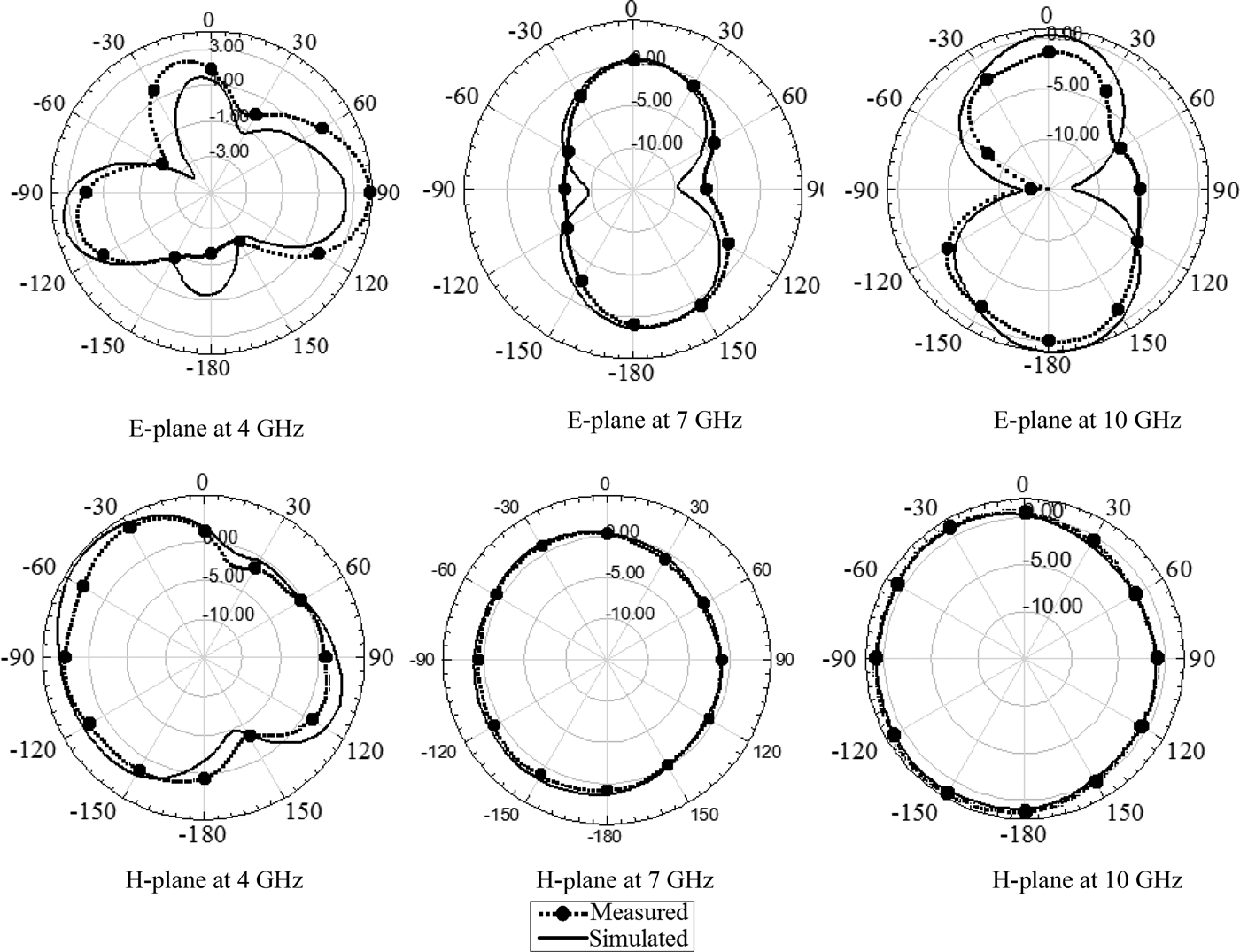
The simulated and measured radiation pattern of fabricated antenna in the UWB mode is shown in Fig. 10. As shown in Fig. 10 the antenna can provide a nearly omnidirectional characteristic in the H-plane and a dipole-like radiation characteristic in the E-plane.
Fig. 10. Simulated and measured radiation patterns in the UWB mode with OFF switches (a) the E-plane and (b) the H-plane.
The gain of UWB antenna and two single band-notch UWB antennas are measured independently using gain comparison method and shown in Fig. 11. In this, the gain is measured in both the planes of the radiation pattern and the peak gain is selected from either plane which gives the larger value. It is clear from Fig. 11 that, the antennas has moderate gain with variations <2.5 dBi throughout the operating band, while the gain drops up to −6 dBi in the notch frequencies. The efficiency of the antenna for both ports is measured using the Wheeler cap method [31] and is also incorporated in Fig. 11. The antenna provides efficiency better than 70% in the UWB spectrum, while it drops to 30% in the notch band.
Fig. 11. Measured peak gain and radiation efficiency of the proposed antenna.
IV. CONCLUSION
In this paper, a UWB antenna with switchable frequency bands for dual band-notched has been introduced for MB-OFDM applications. In addition, the switchable band-notched UWB can eliminate the interference between UWB frequency band and other existing wireless communication systems. This antenna can offer sensing and communicating functions with a small size by controlling ideal switch that is either in the ON or the OFF position. The return loss of the antenna was measured and agreed well with the simulation results. At the same time, the design evolution, equivalent circuit and some critical parameters of the proposed antenna are studied and discussed. The antenna is intended for use in multi-radio wireless applications and future CR communications.
Vahid Sharbati was born in Gorgan, Iran, in 1986. He received the B.S. degree in Electronic Engineering from Hadaf Institute of Higher Education, Sari, Iran, in 2009. Currently, he is working toward the M.S. degree in Communication Engineering from Semnan University. His current research interests are in reconfigurable microstrip antenna for cognitive radio applications.
Pejman Rezaei was born in Tehran, Iran, in 1977. He received the B.S. degree in Communication Engineering from Communication Faculty, Tehran, Iran, in 2000, and the M.S. and Ph.D. degrees from Tarbiat Modarres University, Tehran, Iran, in 2002 and 2007, respectively. His current research interests are in Electromagnetics theory, Antenna, wave propagation, and satellite communication. Currently, he is an Assistant Professor in the Semnan University, Semnan, Iran.
Ali Shahzadi was born in Tehran, Iran, in 1975. He received the B.S. and M.S. degrees in Electronic Engineering from Iran University of Science and Technology (IUST) in 1997 and 2000, respectively, and the Ph.D. degree in Communication Engineering from IUST in 2009. His research interests include the wireless communication, communication security, and statistical digital signal processing. He is currently an Assistant Professor in the Semnan University, Semnan, Iran.
Mohammad M. Fakharian was born in Tehran, Iran, in 1987. He received the B.S. and M. S. degrees in Electric Engineering from Semnan University, Semnan, Iran, in 2009 and 2012, respectively. Currently, he is working toward the Ph.D. degree in Communication Engineering from Semnan University. His research interests include low-profile printed and patch antennas for wireless communication, fractal, miniature and multiband antennas, new materials, meta-materials, and EBG structures interaction with antennas and RF passive components and Electromagnetic theory: numerical methods and optimization techniques.