I. INTRODUCTION
With the tremendous growth in modern wireless communication systems, multiband operations of components and devices are required for different frequency bands associated with different standards and applications, such as the 0.9/1.8/1.9 GHz global systems for mobile communication systems (GSM) bands, the 1.5 GHz global position system (GPS) band, the 2.5/3.5/5.5 GHz worldwide interoperability microwave access (WiMAX) bands, and the 2.4/5.2/5.8 GHz bands of wireless local area networks (WLAN) [Reference Wang, Lu, Meng and Lin1, Reference Yuan, Yin, Ding, Li and Xie2]. Interoperability and co-existence between multi standards is the main critical issue recently. To satisfy this harsh requirement, multi-frequency band operation of components has increasingly become common.
To be used for multiband communication applications and standards, it is required to develop new type of multiband components and devices. Recently, many researches on multiband applications have been presented, such as multiband filter [Reference Herbertz and Lucyszyn3, Reference Tseng and Shao4], Wilkinson power divider, and rat-race coupler. Quarter wavelength transmission line (TL) as the basic element used in Wilkinson power divider and rat-race coupler has been studied and developed for dual or tri-band performance. For example, coupled lines [Reference Park5] and T-type TL [Reference Wu, Liu, Zhang, Gao and Zhou6] have been applied effectively in dual-band Wilkinson power divider; dual-band quarter-wave composite right/left-handed TL (CRLH TL) is presented and applied in rat-race coupler [Reference Lin, DeVincentis, Caloz and Itoh7, Reference Chi, Lee and Itoh8]; the C-section together with two TL sections is proposed and synthesized for dual-band rat-race coupler [Reference Chiou, Kuo and Chan9]; stepped-impedance microstrip line is employed both for multiband Wilkinson power divider [Reference Chongcheawchamnan, Patisang, Krairiksh and Robertson10] and rat-race coupler [Reference Chin, Lin, Wei, Tseng and Yang11]. To design a multiband Wilkinson power divider or rat-race coupler, a simple quarter wavelength TL with multiband performance is the key to find out.
Multiband power amplifiers (PAs) have been presented in previous works also [Reference Edmund Neo12–Reference Wang and Park17]. In traditional multiband PA, parallel path structure with switches has been used [Reference Edmund Neo12]. However, the parallel path structure requires multiple PAs, so the cost of component is multiple and the size of the whole structure is large. To reduce the number of parallel PAs, as a solution, a reconfigurable matching network (MN) concept has been introduced in [Reference Edmund Neo12–Reference Hur, Lee, Lee, Lim and Laskar14]. However, with this technology, switches or electronic tunable elements are required for additional signal control and they may introduce distortions [Reference Kalim and Negra15]. Because of switch or varactor, the multiband performances of PA are unable to be realized simultaneously. Multiband PA using one transistor and one branch of MN without switches or varactor becomes a major solution for multiband purpose recently [Reference Wang and Park16, Reference Wang and Park17]. In the Doherty PA, power divider and quarter wavelength TL are the key element to divide power and to transform impedance [Reference Kim, Moon, Kim, Jee, Son and Kim18]. For the application of multiband Doherty PA, multiband Wilkinson power divider is required to combine the multiband carrier PA and peaking PA, and multiband quarter wavelength TLs are required to transform impedance at the tail of multiband Doherty PA.
Our objective is to develop the Pi-shaped structure to be used as the quarter wavelength TL at each operating frequency for multiband applications [Reference Wang and Park19]. This work is general in terms of number of the operating frequency bands and can be applied in different classes of microwave circuits, such as Wilkinson power divider, rat-race coupler, and PA. In Section II, we will present the topology and principle of the proposed multiband Pi-shaped structure in detail. One tri-band Wilkinson power divider and one tri-band rat-race coupler with compact size are designed, fabricated, and tested in Section III for the demonstration.
II. ANALYSIS OF MULTIBAND PI-SHAPED STRUCTURE
In this section, the proposed multiband (n-band, n ≥ 3) Pi-shaped structure will be presented and analyzed. Firstly, the topology and principle of the tri-band (n = 3) Pi-shaped structure will be explained in Section II(A). Secondly, in Section II(B), the topology and principle of the multiband (n-band, n ≥ 3) Pi-shaped structure will be presented.
A) Tri-band Pi-shaped structure
Figure 1(a) shows the topology of the tri-band Pi-shaped structure. Figures 1(b)–1(d) show the equivalent circuit of Fig. 1(a) at frequency f 1, f 2, and f 3, respectively. Figures 1(e)–1(g) show the equivalent TL of Fig. 1(a) at frequency f 1, f 2, and f 3, respectively. Figure 1(h) shows the topologies of Wilkinson power divider and rat-race coupler. In this paper, we choose the operating frequency as f 1 = 2.5, f 2 = 1.5, and f 3 = 1 GHz. The resonator f 1 and f 2 in Fig. 1(a) are designed with the resonant frequency f 1 and f 2, respectively. The analysis procedure of the tri-band Pi-shaped structure is shown below:

Fig. 1. The principle of the tri-band Pi-shaped structure: (a) the topology of the tri-band Pi-shaped structure, (b–d) the equivalent circuit of (a), (e–g) the equivalent TL of (a), (h) the topologies of Wilkinson power divider and rat-race coupler.
1) AT FREQUENCY F 1 (2.5 GHZ)
At frequency f 1, in Fig. 1(a), because the resonator f 1 has the resonant frequency f 1, its impedance at frequency f 1 is infinite ideally. So, input signal f 1 is blocked by the first resonators f 1. Therefore, the tri-band Pi-shaped structure shown in Fig. 1(a) will become the equivalent circuit as shown in Fig. 1(b) at frequency f 1. The length and characteristic impedance of the equivalent circuit (Fig. 1(b)) are l 1 and Z 1. At frequency f 1, the equivalent circuit will be used as the quarter wavelength branch in Wilkinson power divider and rat-race coupler as shown in Fig. 1(h), so l 1 is equal to λ1/4 and Z 1 is equal to 70.7 Ω.
2) AT FREQUENCY F 2 (1.5 GHZ)
At frequency f 2, an input signal f 2 is passing through the resonator f 1, after then it is blocked by the resonator f 2. Therefore the tri-band Pi-shaped structure will be the equivalent circuit as shown in Fig. 1(c). The length and characteristic impedance of the open-circuited stubs of the equivalent circuit (Fig. 1(c)) are l 2 and Z 2. As mentioned in Section II(A)(1), for the operating frequency f 1 (2.5 GHz), l 1 = λ1/4, Z 1 = 70.7 Ω. By setting the initial value of Z 2 as 50 Ω at frequency f 2, the ABCD matrix of the equivalent circuit (Fig. 1(c)) will be as the following equation:
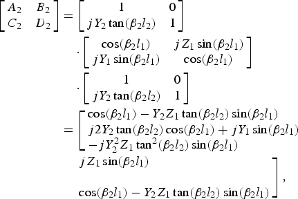 $$\eqalign{\left[\matrix{A_2 & B_2 \cr C_2 & D_2} \right] & =\left[\matrix{ 1 & 0 \cr jY_2 \tan \lpar \beta_2 l_2 \rpar & 1} \right]\cr &\quad \cdot \left[\matrix{\cos \lpar \beta_2 l_1\rpar & jZ_1 \sin \lpar \beta_2 l_1\rpar \cr jY_1 \sin \lpar \beta_2 l_1 \rpar & \cos \lpar \beta_2 l_1\rpar } \right]\cr &\quad \cdot \left[\matrix{1 & 0 \cr jY_2 \tan \lpar \beta_2 l_2 \rpar & 1} \right]\cr & = \left[\matrix{\cos \lpar \beta _2 l_1 \rpar - Y_2 Z_1 \tan \lpar \beta_2 l_2 \rpar \sin \lpar \beta _2 l_1\rpar \cr j2Y_2 \tan \lpar \beta_2 l_2\rpar \cos \lpar \beta_2 l_1\rpar + jY_1 \sin \lpar \beta_2 l_1\rpar \cr - jY_2^2 Z_1 \tan^2 \lpar \beta_2 l_2\rpar \sin \lpar \beta_2 l_1\rpar} \right. \cr &\left. \quad \matrix{jZ_1 \sin \lpar \beta_2 l_1\rpar \cr {}\cr \cos \lpar \beta_2 l_1\rpar - Y_2 Z_1 \tan \lpar \beta_2 l_2\rpar \sin \lpar \beta_2 l_1\rpar }\right]\comma \; }$$
where  $\beta _2=\displaystyle{{2\pi } \over {\lambda _2 }}\comma \; \quad Z_1=70.7\left[\Omega \right]\comma \; \quad l_1=\displaystyle{{\lambda _1 } \over 4}\comma \; \quad Z_2=50\left[\Omega \right].$
At frequency f 2, the equivalent TL of Fig. 1(a) will be as shown in Fig. 1(f). To be used as a branch of Wilkinson power divider and rat-race coupler as shown in Fig. 1(h), the ideal length and characteristic impedance (Z 02) of the equivalent TL should be λ 2/4 and 70.7 Ω at frequency f 2. The ABCD matrix of the equivalent TL, which has quarter wavelength at frequency f 2 can be expressed as:
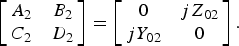 $$\left[{\matrix{ {A_2 } & {B_2 } \cr {C_2 } & {D_2 } \cr } } \right]=\left[{\matrix{ 0 & {jZ_{02} } \cr {jY_{02} } & 0 \cr } } \right].$$
In order to calculate the length l 2 shown in Fig. 1(c) and the characteristic impedance Z 02 of the equivalent TL shown in Fig. 1(f), we equalize equations (1) and (2) and we can deduce:
 $$ \Rightarrow Z_1 \tan \, \lpar \beta _2 l_1 \rpar =Z_2 \cot \, \lpar \beta _2 l_2 \rpar \comma \;$$
 $$ \Rightarrow Z_{02}=Z_1 \sin \, \lpar \beta _2 l_1 \rpar.$$
At frequency f 2 (1.5 GHz), the characteristic impedance Z 02 of the equivalent TL (Fig. 1(f)) is obtained as 57.19 Ω by using equation (4). To use this equivalent TL as a quarter wavelength branch of Wilkinson power divider and rat–race coupler, the ideal value of Z 02 should be 70.7 Ω. To increase the value of Z 02 up to 70.7 Ω instead of 57.19 Ω, we need to increase Z 1 according to equation (4). But Z 1 has already been determined for frequency f 1, so it should be compromise by doing trade-off between Z 1 and Z 02 to satisfy both frequency f 1 and f 2. After fixing the values of Z 1, β 2, l 1, and Z 2, the value of l 2 can be calculated using equation (3).
3) AT FREQUENCY F 3 (1 GHZ)
At frequency f 3, input signal f 3 can pass through the resonator f 1 and resonator f 2. The tri-band Pi-shaped structure shown in Fig. 1(a) becomes the equivalent circuit as shown in Fig. 1(d). The ABCD matrix of the equivalent circuit at frequency f 3 will be as equation (5), where the values of Z 1 and l 1 are as 70.7 Ω and λ 1/4, those are already determined in Section II(A)(1). The initial value of Z 2 has been given in Section II(A)(2) as 50 Ω.
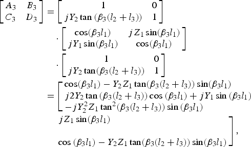 $$\eqalign{\left[\matrix{A_3 & B_3\cr C_3 & D_3} \right]& =\left[\matrix{ 1 & 0 \cr jY_2 \tan \, \lpar \beta _3 \lpar l_2+l_3 \rpar \rpar & 1} \right]\cr &\quad \cdot \left[\matrix{\cos \lpar \beta_3 l_1\rpar & jZ_1 \sin \lpar \beta_3 l_1\rpar \cr jY_1 \sin \lpar \beta _3 l_1 \rpar & \cos \lpar \beta_3 l_1\rpar }\right]\cr &\quad \cdot \left[\matrix{1 & 0 \cr jY_2 \tan \lpar \beta _3 \lpar l_2+l_3 \rpar \rpar & 1 }\right]\cr & = \left[\matrix{\cos \lpar \beta _3 l_1 \rpar - Y_2 Z_1 \tan \lpar \beta _3 \lpar l_2+l_3 \rpar \rpar \sin \lpar \beta _3 l_1 \rpar \cr j2Y_2 \tan \, \lpar \beta _3 \lpar l_2+l_3 \rpar \rpar \cos \, \lpar \beta _3 l_1 \rpar +jY_1 \sin \, \lpar \beta _3 l_1 \rpar \cr - jY_2^2 Z_1 \tan ^2 \lpar \beta _3 \lpar l_2+l_3 \rpar \rpar \sin \, \lpar \beta _3 l_1 \rpar}\right. \cr & \quad \left. \matrix{jZ_1 \sin \lpar \beta _3 l_1\rpar \cr {}\cr \cos \, \lpar \beta _3 l_1\rpar - Y_2 Z_1 \tan \lpar \beta _3 \lpar l_2+l_3 \rpar \rpar \sin \lpar \beta _3 l_1 \rpar }\right]\comma \; }$$
where  $\beta _3=\displaystyle{{2\pi } \over {\lambda _3 }}\comma \; \quad Z_1=70.7\left[\Omega \right]\comma \; \quad l_1=\displaystyle{{\lambda _1 } \over 4}\comma \; \quad Z_2=50\left[\Omega \right].$
At frequency f 3, the equivalent TL of Fig. 1(a) is shown in Fig. 1(g). To be used as a branch of Wilkinson power divider and rat-race coupler at frequency f 3, the ideal length and characteristic impedance (Z 03) of Fig. 1(g) should be λ3/4 and 70.7 Ω. The equivalent TL with quarter wavelength at frequency f 3 can be expressed as:
 $$\left[{\matrix{ {A_3 } & {B_3 } \cr {C_3 } & {D_3 } \cr } } \right]=\left[{\matrix{ 0 & {jZ_{03} } \cr {jY_{03} } & 0 \cr } } \right].$$
By equalizing (5) and (6), we get
 $$ \Rightarrow Z_1 \tan \, \lpar \beta _3 l_1 \rpar =Z_2 \cot \, \lpar \beta _3 \lpar l_2+l_3 \rpar \rpar \comma \;$$
 $$\Rightarrow Z_{03}=Z_1 \sin \, \lpar \beta _3 l_1 \rpar.$$
At frequency f 3 (1 GHz), the characteristic impedance Z 03 of the equivalent TL in Fig. 1(g) is calculated as 41.56 Ω using equation (8). For the Wilkinson power divider and rat-race coupler application, the idea value of Z 03 is 70.7 Ω. So we need to increase the value of Z 03 up to 70.7 Ω. To do that, the compromise between Z 03 and Z 1 should be made in equation (8). By fixing Z 1, β 3, l 1, and Z 2, the length of the open-circuited stub (l 2 + l 3) in Fig. 1(d) can be calculated by equation (7).
As analyzed before, at each operating frequency the tri-band Pi-shaped structure (Fig. 1(a)) is equal to the quarter wavelength TL (Figs 1(e)–1(g)). So we can apply the tri-band Pi-shaped structure (Fig. 1(a)) as a quarter wavelength branch (Fig. 1(h)) in the power divider and coupler. In addition, l 1 is the length of the tri-band Pi-shaped structure (Fig. 1(a)), so it determines the length of the branch of the power divider and coupler. To reduce the size of the components, we set l 1 equal to the quarter wavelength of the highest operating frequency. As mentioned before, frequency f 1 is 2.5 GHz. By equation (3), by fixing the values of Z 1, l 1, and Z 2, the lower frequency f 2 is, the longer the stub length l 2 (Fig. 1(c)) will be. Because the stub length l 2 at frequency f 2 (Fig. 1(c)) is shorter than the stub length (l 2 + l 3) at frequency f 3 as shown in Fig. 1(d), we have to choose that the frequency f 3 (1 GHz) is lower than the frequency f 2 (1.5 GHz).
The used substrate in this paper is TLX-8 of TACONIC with dielectric constant 2.55 and dielectric thickness 31 mil. For more precise simulation, the highly accurate, scalable measurement-based chip capacitor and chip inductor models of Modelithics Inc. are used. For microstrip applications, the measured models take into account substrate related parasitic effects and effective series resistance (ESR). With the same capacitance and inductance value for the same resonant frequency, the simulated results of the LC resonators using the ideal (parasitic free) component models and the measurement-based component models of Modelithics Inc. are compared in Fig. 2. We can also use electrically narrow microstrip TL (MTL)-type inductor instead of using chip inductor in the LC resonator. The LC resonator composed of chip inductor and chip capacitor has the advantage of compact size and simple design structure. However, the standard values of the components are limited by the manufactures. For the selected components (the measured models of Modelithics, capacitor model: CAP-ATC-0603-101, 0.1 to 100 pF; inductor model: IND-CLC-0603-102, 1.8–390 nH), the resonant frequency range of the LC resonator is 0.02–8.16 GHz. Parallel LC resonator composed of MTL-type inductor and chip capacitor can avoid the limitation of standard value of lumped element provided by the manufacturers and it can reduce the parasitic effect of chip inductor. In this paper, we use the LC resonator composed of chip capacitor and chip inductor for the tri-band Wilkinson power divider, and use the LC resonator composed of chip capacitor and MTL-type inductor for the tri-band rat-race coupler to demonstrate our proposed multiband design method.
Fig. 2. Simulated comparison of the LC resonators designed by using the ideal models and the measured models of Modelithics Inc. with the same value of capacitance and inductance at (a) 1.5 GHz and (b) 2.5 GHz. Solid line, insertion loss; dot, return loss.
In Advanced Design System (ADS) simulation, the optimized simulation parameters of the tri-band Pi-shaped structure (Fig. 1(a)) are shown in Table 1.
Table 1. Optimized simulation parameters of the tri-band Pi-shaped structure in ADS.
The simulated phase result of the tri-band Pi-shaped structure is shown in Fig. 3. At 1, 1.5, and 2.5 GHz, the S 21 phase of the tri-band Pi-shaped structure (Fig. 1(a)) is −89.93°, −89.92°, and −90.10°, respectively.
Fig. 3. The simulated result of phase of the tri-band Pi-shaped structure.
The simulated result of impedance of the tri-band Pi-shaped structure is shown in Fig. 4. The normalized impedance of the Smith chart is 70.7 Ω. At 1.5 GHz, with the load of 70.7 Ω at Port 2 in Fig. 1(a), the impedance at Port 1 (Fig. 1(a)) of the tri-band Pi-shaped structure is 72.8 Ω, whereas the compromised impedances are 36.8 and 135.7 Ω at 1 and 2.5 GHz, respectively. Because the tri-band Pi-shaped structure is equal to the quarter wavelength TL at 1/1.5/2.5 GHz as shown in Fig. 3, the characteristic impedance of the tri-band Pi-shaped structure can be calculated using the single-section quarter-wave matching transformer equation [Reference Pozar20] as 51.0/71.8/98.0 Ω at 1/1.5/2.5 GHz, respectively.
Fig. 4. The simulated result of impedance of the tri-band Pi-shaped structure.
The simulated result of insertion loss S 21 and return loss S 11 of the tri-band Pi-shaped structure is shown in Fig. 5. At the three operating frequencies 1/1.5/2.5 GHz, the insertion loss is less than 0.64 dB and the return loss is better than 10.02 dB.
Fig. 5. The simulated result of insertion loss (solid line) and return loss (dot) of the tri-band Pi-shaped structure.
B) Multiband (n-band, n ≥ 3) Pi-shaped structure
Right now we do a generalization of the multiband (n-band, n ≥ 3) Pi-shaped structure. The topology of the multiband Pi-shaped structure is shown in Fig. 6(a). For the n-band (n ≥ 3) Pi-shaped structure, the number of the resonators in the open-circuited stub at each side is n − 1. The resonator f x(x = 1, …, and n − 1) in Fig. 6(a) is used to block frequency f x while other frequency can pass through it. At frequency f 1 and f 2, as discussed in Section II(A), the equivalent circuit of the multiband Pi-shaped structure is shown in Fig. 6(b) and (c), respectively. At frequency f n(n ≥ 3), the equivalent circuit of Fig. 6(a) is shown in Fig. 6(d). The total length of the open-circuited stub at frequency f n is equal to (l 2 + … + l n) with a characteristic impedance of Z 2.
Fig. 6. The principle of the multiband (n-band, n ≥ 3) Pi-shaped structure: (a) the topology of the multiband Pi-shaped structure, (b–d) the equivalent circuit of (a), (e–g) the equivalent TL of (a).
The ABCD matrix of the equivalent circuit at frequency f n (Fig. 6(d)) is shown as equation (9). As discussed in Section II(A), for the Wilkinson power divider and rat-race coupler applications, we set Z 1 = 70.7 Ω and l 1 = λ1/4 for frequency f 1. The initial value of Z 2 is given as 50 Ω.
 $$\eqalign{\left[\matrix{A_n & B_n\cr C_n & D_n} \right]& =\left[\matrix{ 1 & 0 \cr jY_2 \tan \, \lpar \beta _n \lpar l_2+\cdots+l_n \rpar \rpar & 1} \right]\cr &\qquad \cdot \left[\matrix{\cos \lpar \beta _n l_1\rpar & jZ_1 \sin \lpar \beta _n l_1\rpar \cr jY_1 \sin \, \lpar \beta _n l_1 \rpar & \cos \lpar \beta _n l_1\rpar }\right]\cr &\qquad \cdot \left[\matrix{1 & 0 \cr jY_2 \tan \lpar \beta _n \lpar l_2+\cdots+l_n \rpar \rpar & 1 } \right]\cr & =\left[\matrix{\cos \lpar \beta _n l_1 \rpar - Y_2 Z_1 \tan \lpar \beta _n \lpar l_2+\cdots+l_n \rpar \rpar \sin \, \lpar \beta _n l_1 \rpar \cr j2Y_2 \tan \, \lpar \beta _n \lpar l_2+\cdots+l_n \rpar \rpar \cos \, \lpar \beta _n l_1 \rpar +jY_1 \sin \, \lpar \beta _n l_1 \!\rpar \cr - jY_2^2 Z_1 \tan ^2 \lpar \beta _n \lpar l_2+\cdots+l_n \rpar \rpar \sin \, \lpar \beta _n l_1 \rpar}\right.\cr & \quad \left. \matrix{jZ_1 \sin \, \lpar \beta _n l_1 \rpar \cr {} \cr \cos \, \lpar \beta _n l_1 \rpar - Y_2 Z_1 \tan \lpar \beta _n \lpar l_2+\cdots+l_n \rpar \rpar \sin \lpar \beta _n l_1 \rpar } \right]\comma \; }$$
where  $\beta _n=\displaystyle{{2\pi } \over {\lambda _n }}\comma \; \quad Z_1=70.7\left[\Omega \right]\comma \; \quad l_1=\displaystyle{{\lambda _1 } \over 4}\comma \; \quad Z_2=50\, \lsqb \Omega \rsqb .$
At frequency f n, the ABCD matrix of the equivalent quarter wavelength TL (Fig. 6(g)) can be expressed as:
 $$\left[{\matrix{ {A_n } & {B_n } \cr {C_n } & {D_n } \cr } } \right]=\left[{\matrix{ 0 & {jZ_{0n} } \cr {jY_{0n} } & 0 \cr } } \right].$$
For Wilkinson power divider and rat-race coupler, ideally the equivalent length of the equivalent circuit (Fig. 6(d)) should be λ n/4 at frequency f n. To do that, by equalizing equations (9) and (10), it is deduced:
 $$ \Rightarrow Z_1 \tan \lpar \beta _n l_1 \rpar =Z_2 \cot \lpar \beta _n \lpar l_2+\cdots+l_n \rpar \rpar \comma \;$$
 $$\Rightarrow Z_{0n}=Z_1 \sin \, \lpar \beta _n l_1 \rpar.$$
At frequency f n, the equivalent characteristic impedance Z 0n should be approached 70.7 Ω for Wilkinson power divider and rat-race coupler by trading off between Z 0n and Z 1 using equation (12). By fixing the value of Z 1, β n, l 1, and Z 2, the length of the open-circuited stub (l 2 + … + l n) can be obtained with equation (11).
III. FABRICATION AND MEASUREMENT
A) Tri-band Wilkinson power divider
To demonstrate the proposed multiband design method, by using multiband Pi-shaped structure in Section II, we fabricated one tri-band Wilkinson power divider. The topology and fabricated circuit of the tri-band Wilkinson power divider are shown in Fig. 7. To reduce the size of the circuit, we put all stubs inside the tri-band Wilkinson power divider itself.
Fig. 7. The topology (a) and fabricated circuit (b) of the tri-band Wilkinson power divider.
The LC resonators f 1 and resonators f 2 in Fig. 7 are composed of chip capacitor and chip inductor. The ideal resonant frequency of LC resonator can be calculated using equation (13), where f 0 is the resonant frequency, L is the inductance of inductor, and C is the capacitance of capacitor. The resonant frequency (f 0) of LC resonator increases or decreases while the product of L and C decreases or increases. The resonator f 1 in Fig. 7 has the resonant frequency of 2.5 GHz. As shown in Table 1, the initial capacitance value of the used ATC capacitor model of Modelithics Inc. for the resonator f 1 is 0.8 pF. Figure 8 shows the simulated comparison of the tri-band Wilkinson power divider by only changing the capacitance value of the capacitors in the resonators f 1 in Fig. 7. Because the capacitance value of the resonators f 1 reduces, the highest operating frequency band (2.5 GHz) shifts to a higher frequency band region. To increase the bandwidth of the middle operating frequency band (1.5 GHz) and have a better performance at 2.5 GHz, we reduced the capacitance value of the capacitor models in the resonators f 1 from 0.8 to 0.4 pF as shown in Fig. 8. Figure 9 shows the simulated comparison of the tri-band Wilkinson power divider by only changing the capacitance value of the capacitors in the resonators f 2 in Fig. 7. Because the resonator f 2 has a resonant frequency of 1.5 GHz, it affects the middle operating frequency band (1.5 GHz). As shown in Fig. 9, the middle operating frequency band (1.5 GHz) shifts to be higher and the bandwidth of the lowest operating frequency band (1 GHz) increases when the capacitance value in the resonators f 2 reduces. The final used capacitance and inductance value in the resonators f 1 and resonators f 2 for the tri-band Wilkinson power divider is 0.4 pF and 3.6 nH, and 1.8 pF and 5.1 nH, respectively.
 $$f_0=\displaystyle{1 \over {2\pi \sqrt {{\rm LC}} }}.$$
Fig. 8. Simulated comparison of the different capacitance values in the resonators f 1 in Fig. 7: (a) insertion loss of S 21 and S 31, (b) isolation of S 32, (c) input return loss of S 11, (d) output return loss of S 22 and S 33. Solid line, 0.4 pF; dot, 0.1 pF; and short dash, 0.8 pF.
Fig. 9. Simulated comparison of the different capacitance values in the resonators f 2 in Fig. 7: (a) insertion loss of S 21 and S 31, (b) isolation of S 32, (c) input return loss of S 11, (d) output return loss of S22 and S33. Solid line, 1.8 pF; dot, 1.5 pF; and short dash, 2 pF.
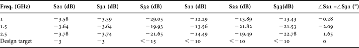
The simulated and measured results of the tri-band Wilkinson power divider are compared from Figs 10–13. The measured insertion loss at 1/1.5/2.5 GHz is less than 3.78 dB, input and output return loss is more than 12.29 dB, and output isolation is better than 19.93 dB. The simulated results are consistent with the measured results. The measured phase difference between the two output ports is less than 2.1° as shown in Fig. 24 (solid line).
Fig. 10. Simulated (x) and measured (round and triangle) insertion loss of the tri-band Wilkinson power divider.
Fig. 11. Simulated (x) and measured (round) output port isolation of the tri-band Wilkinson power divider.
Fig. 12. Simulated (x) and measured (round) input return loss of the tri-band Wilkinson power divider.
Fig. 13. Simulated (x) and measured (round and triangle) output return loss of the tri-band Wilkinson power divider.
In Fig. 10, the measured insertion loss S 21 and S 31 at 1/1.5 /2.5 GHz is 3.58/3.64/3.78 and 3.59/3.64/3.74 dB, respectively.
In Fig. 11, the measured isolation S 32 at 1/1.5 /2.5 GHz is 29.05/19.93/21.65 dB.
In Fig. 12, the measured input return loss S 11 at 1/1.5 /2.5 GHz is 12.29/13.56/14.49 dB.
In Fig. 13, the measured output return loss S 22 and S 33 at 1/1.5/2.5 GHz is 13.89/21.82/19.49 and 13.43/21.53/22.78 dB, respectively.
Comparing the simulated and measured results, there is a slight difference between them. The authors consider the difference comes from the tolerance of the used components. For the used ATC 600S 0.4 pF capacitor, the tolerance is ±0.1 pF; for the used ATC 600S 1.8 pF capacitor, the tolerance is ±0.25 pF; for the used Coilcraft 0603 inductor, the tolerance is 2%.
The measured results of the tri-band Wilkinson power divider are summarized in Table 2.
Table 2. Measured results of the tri-band Wilkinson power divider.
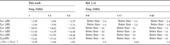
The tri-band Wilkinson power divider in this work is compared with the work of Chongcheawchamnan et al. [Reference Chongcheawchamnan, Patisang, Krairiksh and Robertson10] as shown in Table 3. Chongcheawchamnan et al. [Reference Chongcheawchamnan, Patisang, Krairiksh and Robertson10] show a tri-band Wilkinson power divider with the excellent and wideband performance. Being different from the reference, our work presents a relative narrow-band type and intrinsically multiband Wilkinson power divider. The signal between the desired operating bands is well attenuated to avoid the potential interference between each operating frequency band. The proposed tri-band Wilkinson power divider in this work can be used for concurrent multiband PA applications. The size of the tri-band Wilkinson power divider in this work is 29 mm × 32 mm compared with the size of the power divider presented in [Reference Chongcheawchamnan, Patisang, Krairiksh and Robertson10] which is 31 mm × 55 mm. For the future work, the authors are considering increasing the operating frequency bandwidth by employing microstrip radial stub (MRS) according to its wideband characteristic [Reference Wang and Park21].
Table 3. Comparison between this work and the work of [Reference Chongcheawchamnan, Patisang, Krairiksh and Robertson10].
B) Tri-band rat-race coupler
The topology and fabricated circuit of the proposed tri-band rat-race coupler are shown in Fig. 14. In the fabricated tri-band rat-race coupler, we used the thin MTL-type inductor instead of a chip inductor to avoid the limited standard inductance values provided by the manufacturers. To keep the compactness of the tri-band rat-race coupler, all stubs with resonators are putted inside the circuit itself.
Fig. 14. The topology (a) and fabricated circuit (b) of the tri-band rat-race coupler.
In Fig. 14, the initial capacitance value of the capacitors in the resonators f 1 is 1.2 pF, and that of the capacitors in the resonators f 2 is 2.7 pF. The resonator f 1 composed of the chip capacitor and the MTL-type inductor has the resonant frequency of 2.5 GHz. Figures 15 and 16 show the simulated comparisons of only changing the capacitance value of the resonators f 1 in the tri-band rat-race coupler. By decreasing the capacitance value of the resonators f 1, the bandwidth of the middle operating frequency (1.5 GHz) can be increased and the highest operating frequency band (2.5 GHz) will shift to a higher band region. The resonators f 1 do not affect the performance of the lowest frequency band (1 GHz). Figures 17 and 18 show the simulated comparisons of only changing the capacitance value of the resonators f 2 in Fig. 14. The resonator f 2 has the resonant frequency of 1.5 GHz. It affects the performance of the middle operating frequency band (1.5 GHz). As Figs 17 and 18 show us, if the capacitance value of the resonators f 2 decreases, the middle operating frequency band (1.5 GHz) shifts to be higher, whereas the highest operating frequency band (2.5 GHz) being affected little. The final used capacitance values of the capacitors in the resonators f 1 and the resonators f 2 in the tri-band rat-race coupler are 1.2 and 2.7 pF, respectively.
Fig. 15. Simulated comparison of insertion loss of using the different capacitance values in the resonators f 1 in Fig. 14, (a) S 23, (b) S 43, (c) S 21, (d) S41. Solid line, 1.2 pF; dot, 1 pF; and short dash, 1.5 pF.
Fig. 16. Simulated comparison of return loss and isolation of using the different capacitance values in the resonators f 1 in Fig. 14: (a) S 11 and S 44, (b) S 22 and S 33, (c) S 31 and S 42. Solid line, 1.2 pF; dot, 1 pF, and short dash, 1.5 pF.
Fig. 17. Simulated comparison of insertion loss of using the different capacitance values in the resonators f 2 in Fig. 14: (a) S 23, (b) S 43, (c) S 21, (d) S 41. Solid line, 2.7 pF; dot, 2.2 pF; and short dash, 3.3 pF.
Fig. 18. Simulated comparison of return loss and isolation of using the different capacitance values in the resonators f 2 in Fig. 14: (a) S 11 and S 44, (b) S 22 and S 33, (c) S 31 and S 42. Solid line, 2.7 pF; dot, 2.2 pF; and short dash, 3.3 pF.
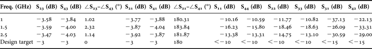
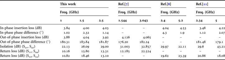
The simulated and measured results of the fabricated tri-band rat-race coupler are compared from Figs 19–23. At 1/1.5/2.5 GHz, the measured results show that the insertion loss is less than 4.04 dB, the return loss is better than 10.16 dB; and the isolation between Ports 1 and 3, and Ports 2 and 4 are better than 26.09 and 22.13 dB, respectively. As shown in Fig. 24, in-phase difference ∠S 23 − ∠S 43 is less than 2.32°, and out-of-phase difference ∠S 21 − ∠S 41 is less than 183.84°. The measured results of the tri-band rat-race coupler in this paper are compared with the dual-band rat-race couplers proposed in [Reference Lin, DeVincentis, Caloz and Itoh7, Reference Chi, Lee and Itoh8, Reference Chin, Lin, Wei, Tseng and Yang11] as shown in Table 5. The results are comparable. However, the proposed multiband design method in this paper is more general in terms of number of the operating frequency bands. As mentioned in the end of Section III(A), the authors are considering increasing the bandwidth of each operating frequency band by using MRS instead of using microstrip rectangular stub.
Fig. 19. Simulated (x and cross) and measured (round and triangle) insertion loss of S 23 and S 43 of the tri-band rat-race coupler.
Fig. 20. Simulated (x and cross) and measured (round and triangle) insertion loss of S 21 and S 41 of the tri-band rat-race coupler.
Fig. 21. Simulated (x and cross) and measured (round and triangle) return loss of Ports 1 and 4 of the tri-band rat-race coupler.
Fig. 22. Simulated (x and cross) and measured (round and triangle) return loss of Ports 2 and 3 of the tri-band rat-race coupler.
Fig. 23. Simulated (x and cross) and measured (round and triangle) isolation of S 31 and S 42 of the tri-band rat-race coupler.
Fig. 24. Measured phase difference of output ports of the tri-band Wilkinson power divider (solid line) and tri-band rat-race coupler (dot and dash).
Table 4. Measured results of tri-band rat-race coupler.
In Fig. 19, the measured in-phase insertion loss S 23 and S43 at 1/1.5 /2.5 GHz is 3.58/3.59/3.47 and 3.84/4.00/4.03 dB, respectively. The measured in-phase difference at 1/1.5/2.5 GHz is 1.02°/2.32°/1.14° as shown in Fig. 24 (dash).
In Fig. 20, the measured out-of-phase insertion loss S 21 and S 41 at 1/1.5/2.5 GHz is 3.77/3.87/3.92 and 3.88/4.04/3.87 dB, respectively. The measured out-of-phase difference at 1/1.5/2.5 GHz is 180.31°/183.84°/181.87° as shown in Fig. 24 (dot).
In Fig. 21, the measured return loss S 11 and S 44 at 1/1.5/2.5 GHz is 10.16/16.23/13.38 and 10.59/15.80/13.31 dB, respectively.
In Fig. 22, the measured return loss S 22 and S 33 at 1/1.5/2.5 GHz is 11.77/18.46/14.75 and 10.82/18.63/13.10 dB, respectively.
In Fig. 23, the measured isolation S 31 and S 42 at 1/1.5/2.5 GHz is 37.13/26.09/30.59 and 22.13/33.31/29.00 dB, respectively.
The measured results of the tri-band rat-race coupler are summarized in Tables 4 and 5.
Table 5. Comparison between this work and the works of [Reference Lin, DeVincentis, Caloz and Itoh7], [Reference Chi, Lee and Itoh8], and [Reference Chin, Lin, Wei, Tseng and Yang11].
IV. CONCLUSION
This paper presents a novel Pi-shaped structure for multiband applications. For the first time, the multiband (n-band, n ≥ 3) Pi-shaped structure which is equal to multiband quarter wavelength TL has been investigated and analyzed by employing ABCD matrix. Resonators are used in the multiband Pi-shape structure to select operating frequency. This proposed Pi-shaped structure can be applied in multiband Doherty PA for its Wilkinson power divider and quarter wavelength TLs. To demonstrate the proposed multiband design method, at three frequencies 1/1.5/2.5 GHz, one tri-band Wilkinson power divider and one tri-band rat-race coupler are designed, fabricated, and tested. The compactness of the demonstrated circuits is kept by putting all stubs with resonators inside the circuits themselves. In addition, by choosing the series circuit element in the highest operating frequency, the total size of the demonstrated circuits is smaller than the single band circuit designed for the lower frequency. The excellence performance of the proposed multiband circuits is shown both by measurement and simulation. The multiband design method proposed in this paper can be widely applied in multiband applications.
 Zhebin Wang was born in Nantong, Jiangsu province, China. He received the B.Sc. degree from Nanjing University of Information Science & Technology (NUIST), Jiangsu, China, in 2008. He obtained the M.Sc. degree in Electrical Engineering from University of Quebec in Rimouski (UQAR), Quebec, Canada, in 2013. His research interests are high-efficiency power amplifiers and circuits for multiband applications. In 2012, he won the second place in the “2012 IEEE MTT-S International Microwave Symposium Student High Efficiency Power Amplifier Design Competition” in IEEE MTT-S International Microwave Symposium (IMS2012) hold in Montreal, Canada.
 Chan-Wang Park has received the B.Sc. degree in Electronic and Communication Engineering from Han Yang University, in Seoul, Korea in 1981 and M.Sc. degree from E.N.S.T. de Paris in France and Ph.D. degree from IEMN, Université des sciences et technologies de Lille 1 in France 1996 and 2001, respectively. From 1981 to 1985 he was in R&D center with Gold Star Electric (L.G. Telecom) at AnYang in Korea. From 1985 to 1990 he was in Training Centre in Saudi Telecom as a Technical Instructor. From 1990 to 1994 he developed three satellites at Satellite Technology Research Centre in KAIST, in Korea as a project manager. From 1994 to 1995 he was with IAS and Matra Marconi Space in France. From 2001 to 2002 he was with AmpliX and Mitec Telecom in Canada. In 2003, he joined the Université du Québec à Rimouski, where he is currently a professor. His research area is high power amplifier design, a characterization of transistor and RF/microwave and millimeter wave components design.