


I. INTRODUCTION
The wurtzite materials AlN and ZnO are currently the only piezoelectrics that are used in thin-film form for microwave applications in the 1–10 GHz range. They combine good piezoelectric properties with excellent acoustic qualities, and grow most easily in the optimal film orientation for RF filter applications. In addition, they can be synthesized by sputter deposition, a plasma method allowing for low processing temperatures. According to Hickernell [Reference Hickernell1], efforts to grow ZnO thin films go back to around 1965; good-quality films were obtained in the mid- to late 1970s, mostly by sputtering [Reference Khuri-Yakub, Kino and Galle2, Reference Yamamoto, Shiosaki and Kawabata3], but also by CVD [Reference Shiosaki, Ohnishi, Kirokawa and Kawabata4]. Besides electro-acoustic applications, optical applications [Reference Shiosaki, Ohnishi, Kirokawa and Kawabata4] were also investigated. The potential of these films for RF filtering with bulk acoustic waves (BAWs) was soon discovered [Reference Grudkowski, Black, Reeder, Cullen and Wagner5–Reference Nakamura, Sasaki and Shimizu7]. Such devices are composed of several electromechanical resonators, commonly called thin-film bulk acoustic resonators (TFBARs), which are based on standing bulk waves trapped in a film slab, as sketched in Fig. 1, whereby film thickness defines the frequency of resonance. In these early years, ZnO was much more frequently investigated than AlN. Insufficient vacuum in the deposition tools at this time is certainly one of the reasons, because nitrides require much better vacuum conditions than oxides. In addition, the target applications had frequencies in the ultra-high frequency range (television), requiring a film thickness of several micrometers. This is not ideal for a material such as AlN that tends to create immense mechanical stresses, and also exhibits a very high sound velocity requiring almost twice as thick layers as with ZnO. Anyhow, the time was not yet ripe for TFBARs. Surface acoustic wave (SAW) devices based on piezoelectric single crystals such as quartz, LiNbO3, and LiTaO3 were and are much more practical in the frequency range below 1 GHz. SAW filter production was much less demanding, once single-crystal wafers of these materials were available. TFBARs had to wait until the mid-1990s for the first industrial activities [Reference Lakin, Kline and McCarron8, Reference Lakin, McCarron and Rose9]. Sputter sources and industrial-type vacuum systems were considerably improved in the meantime, MEMS technology was already at a suitable development stage, and then the application was ready as well: mobile communication. Especially the second generation with carrier frequencies around 2 GHz was and still is ideal for TFBARs, because the required thin-film thickness is in a reasonable range. After the year 2000, TFBAR filters for mobile phones entered industrial production on a larger scale, first as membrane structures [Reference Ruby, Bradley, Oshmyansky, Chien and Larson10] and later also with acoustic reflectors [Reference Aigner, Kaitila, Ellia, Elbrecht, Nessler, Handmann, Herzog and Marksteiner11, Reference Heinze, Schmidhammer, Diekmann and Metzger12]. BAW filters are especially suited to obtain passbands with very sharp drops to large rejection at the band edge, as is possible with the so-called ladder filter design. This is the desired property for duplex filters. They provide RF filtering on the Rx and Tx bands, while keeping a minimal frequency separation between the bands. Today, AlN is in most, or even in all, cases the preferred material for TFBARs. The first reason is that the relevant properties of AlN are sufficient to reach specifications for RF filters in mobile telecommunication. In addition, AlN can handle higher power levels than ZnO because its thermal conductivity is larger and its dielectric losses are lower. Furthermore, its chemical composition complies with semiconductor fabrication requirements, and thus constitutes the ideal material for above-IC integration. First, above-IC integration of AlN FBAR filters has been successfully demonstrated in planar integration on GaAs devices [Reference Cushman, Lau, Garber, Mai, Oki and Kobayashi13], and more recently in vertical integration above Si ICs [Reference Dubois, Carpentier, Vincent, Billard, Parat, Muller, Ancey and Conti14].

Fig. 1. Schematic drawing of a bulk acoustic resonance in a piezoelectric plate. The vertical dimension is very exaggerated. In the vibrating, active zone, the pressure amplitude for the fundamental mode is sketched. The trapped wave has half the wavelength within the slab thickness.
TFBARs exploit the fundamental, thickness extensional mode of a piezoelectric plate that is much wider than thick, as schematically drawn in Fig. 1. The amplitude of this mode points along the z-direction. The strains in the layer plane are zero [Reference Ikeda15], because lateral displacements cannot follow the thickness vibration. The relation between materials properties, microstructures, dimensions, and final properties is quite complex. Nonetheless, it has always been a major goal of device development to understand the underlying microstructure–property relations of the involved materials [Reference Hickernell1], and to characterize as much as possible on the level of single layers in order to be able to predict device properties of the actual multilayer resonators. Of course, nothing can replace the evaluation of resonators. Only these can finally yield the correct coupling constants and quality factors. It is however important for research and development to apprehend specific features of process–microstructure relations that are important for properties. This advances the understanding of basic mechanisms that eventually can be generalized. In addition, it is useful to dispose of measurement techniques that allow the assessment of properties before full device fabrication. The motivation for further research in this area arises from the need to improve the current performance of RF filters. Even relatively small improvements in coupling and quality factor might be paying in terms of filter characteristics and commercial success. In addition, there are further ideas for applications, for instance in the direction of microwave oscillators [Reference Masson, Martin, Boudot, Gruson, Ballendras, Artieda, Muralt, Belgacem and Chomemeloux16, Reference Artieda and Muralt17]. In their case, high-quality factors and temperature stability are crucial parameters. A very actual topicis the search for tuning possibilities. The tuning of frequencies could allow for a reduction in the number of filters in mobile phones.
In the following, some issues in the characterization of TFBARs and their materials are discussed. AlN is discussed in more detail while trying to find an answer to the question of how good AlN really is. This question is related to optimal substrates and microstructures. Later, the case of ferroelectrics is briefly presented, interesting for tunable filters. In this case, the control of microstructure in the large sense is very important.
II. PROPERTIES OF ALN AND ZNO
The two materials properties of primary interest in making wide band filters are coupling factor k t2 – defining the elastic energy stored in the plate for a given input electrical energy – and quality factor Qm of the piezoelectric and further involved materials. The effective values obtained from a resonator characteristic depend on other features of the device, such as electrode properties.
For optimal coupling in a parallel plate capacitor, the polar c-axis of wurtzite structures must be grown perpendicular to the device plane, i.e. along z in Fig. 1. The piezoelectric coupling is then expressed in terms of material properties as:
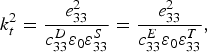
where e 33, c 33E, and ɛ33S are piezoelectric coefficient, stiffness at constant electric field (E) (or at constant displacement field D), and relative permittivity at constant strain S (or at constant stress T), respectively.
The quality factor of materials is limited by viscous losses [Reference Ballato and Gualtieri18]. The elastic constants have an imaginary part proportional to viscosity η, with the same tensorial properties as stiffness:
A time constant τ1 can be defined as τ1 = η/c, using the relevant stiffness constants c for the vibration mode in question, and the quality factor is then written as:
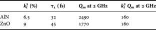
The product k t2Q m is introduced as a figure of merit for optimal resonator characteristics. (The ratio of the maximal to the minimal peak values of the impedance |Z| is proportional to k 2Q of the resonator.) Using standard literature values for AlN and ZnO, the values for k t2 and Qm are obtained as given in Table 1. This table shows that ZnO and AlN are approximately equivalent in terms of k 2Q. In practice, this figure of merit amounts to 50 to 100 rather than to 160. The table thus suggests that improvements are still possible. Other criteria may, however, become very important as well. Filters in the transmission line must survive high power densities. It turns out that AlN can withstand larger voltages without break-down, and exhibits lower leakage currents than ZnO. In addition, AlN is a better heat conductor than ZnO. All these properties contribute to better power handling with AlN resonators.
Table 1. Relevant materials parameters for TFBAR applications for the two most used wurtzite thin films, as derived from standard literature data [Reference Ballato and Gualtieri18, Reference Gualtieri, Kosinski and Ballato19].
III. IS PERFORMANCE OF ALN BETTER THAN EXPECTED? PREDICTIONS FROM MICROSTRUCTURE–PROPERTY RELATIONS
Our knowledge on the piezoelectric properties of pure AlN stems mainly from thin films. There are no single-crystal reference data for the simple reason that the growth of perfect single crystals has not been mastered yet. The measured piezoelectric properties of crystals do not reach those of thin films [Reference Bu, Ciplys, Shur, Schowalter, Schujman and Gaska20]. For a long time, properties evaluated at SAW structures of epitaxial single crystalline films grown at high temperature served as standard values [Reference Tsubouchi and Mikoshiba21]. Recent work indicates that the piezoelectric coefficients are probably larger. A discrepancy exists especially with thin-film piezoelectric measurements based on interferometric techniques [Reference Martin, Muralt, Dubois and Pezous22]. These measure the so-called clamped piezoelectric coefficient:
Likewise, one usually measures an “unclamped” transverse coefficient e31,f, unclamped because the film is free to move along the vertical direction z, perpendicular to the film plane (crystal direction three as well):
In Table 2, standard values are compared with recently published results from ab initio calculations [Reference Kamiya23], direct measurements of piezoelectric coefficients of polycrystalline textured films [Reference Martin, Muralt, Dubois and Pezous22] (see Fig. 4), and coupling coefficient measurements of resonators of similar films [Reference Löbl, Klee, Metzmacher, Brand, Milsom and Lok24]. These recent works strongly suggest that the piezoelectric coefficients of thin films are larger than expected to date. The d33,f value for very narrow rocking curve widths is extrapolated as 6.8 pm/V. This corresponds to kt2 values of 8–9%. This value agrees very well with the extrapolated kt2 of Löbl et al. [Reference Löbl, Klee, Metzmacher, Brand, Milsom and Lok24], where the coupling is depicted as a function of rocking curve width.
Table 2. Materials constants of AlN from different sources. Standard data from epitaxial films on sapphire are compared to ab initio calculations and data from polycrystalline thin films (bold: primary data; italics: derived data).

The high-quality performance of polycrystalline thin films is not at all evident, given the polycrystalline microstructure (Fig. 2). However, the grains are very crystalline and oriented, as shown by the transmission electron microscopy (TEM) image and corresponding diffraction patterns (Fig. 3). In case of Pt (111) electrodes with their hexagonal (111) surface planes, the hexagonal AlN structure tends to nucleate epitaxially on each Pt grain, thereby promoting (001) growth of AlN. However, this mechanism is not necessary to achieve (001) growth. This orientation can also be obtained on amorphous substrates. The crucial process parameter is rather the energy of bombarding positive ions originating from the sputter plasma [Reference Dubois and Muralt27]. There is interesting evidence from different deposition methods that (001) growth is promoted by ion bombardment of energies in the range 20–40 eV, as evidenced by arc deposition [Reference Takikawa, Kuimura, Miyano, Sakakibara, Bendavid, Martin, Matsumuro and Tsutsumi28] and RF sputtering [Reference Drusedau and Blasing29]. However, it is not precisely known what this bombardment is effectively doing on the level of atoms, apart from promoting surface diffusion.

Fig. 2. Dark-field TEM image showing an AlN(001) thin film on a Pt(111) electrode. The epitaxial growth on single Pt grains is well visible (film as described in ref. [Reference Martin, Muralt, Dubois and Pezous22]).
Usually, rocking curve width is interpreted in terms of tilted c-planes. This tilt would then directly result from the roughness of the substrate, given that the first atomic plane of a nucleus is defined by substrate surface. The tilt by a few degrees cannot explain, however, why the piezoelectric effect should be reduced so drastically. For small tilt angles α, the piezoelectric coefficient e 33 should vary as:

The upper index 0 indicates the standard piezoelectric coefficients with no tilt between E-field and c-axis. The values of the e-coefficients were taken from ref. [Reference Gualtieri, Kosinski and Ballato19]. This effect should not even be visible on the value scale of Fig. 4. The discrepancy was also raised for a similar investigation dealing with the d 31 coefficient of ZnO films in beam structures [Reference Gardeniers, Rittersma and Burger30]. The reason is thus completely different. A further argument against a direct relation of tilt and polar ordering is the fact that the growth of piezoelectric AlN with a homogeneously tilted c-axis is possible [Reference Bjurstrom, Rosen, Katardjiev, Yanchev and Petrov31–Reference Bjurstrom, Wingqvist and Katardjiev33], in spite of tilt angles being much larger than 5°. The direction of the polar axis matters, quite obviously. The sign of piezoelectricity is linked to the direction of this axis, meaning that we should make the difference between (0, 0,+1) and (0, 0,−1) orientations. A 1:1 mixture of these orientations yields zero piezoelectric effect. The mechanism that is responsible for the polarity choice is not well understood for low-temperature growth by sputtering. In high temperatures, for instance on sapphire at 900–1000°C, the orientation is certainly imposed by interface and surface energies that are advantageous for one of the polarities.
This effect cannot be the only mechanism at low temperatures. Ion bombardment and further plasma impacts (there is also electron bombardment) certainly play a role in polarity choice, because the energy of bombarding ions plays a role.
There is also evidence that substrate chemistry may play a role. Ruffner et al. [Reference Ruffner, Clem, Tuttle, Dimos and Gonzales36] found an influence of Ru electrode preparation, i.e. the degree of oxidation of Ru that leads to values ranging from −3.5 to +4 pm/V. The correlation with rocking curve widths would mean that the more perfect the growth approaches a kind of one-dimensional single-crystal growth with very extended c-planes, the better the relatively weak effect of mobility enhancement by plasma impact is able to promote one of the two polarities. Accordingly, one should interpret the rocking curve width as a correlation length issue rather than as a tilt issue. This is shown in Fig. 5, where d 33,f is plotted against the correlation L // , with the same data points as in Fig. 4. This figure suggests that there is an asymptotic value of around 6 pm/V that is approached for large correlation lengths, and that the curve might well start at zero for very thin AlN films of a few atomic layers. Thicker films show a larger correlation length. The values of L// correspond not too badly with the fiber-grain diameter, and thus with the in-plane grain boundary distance (see Fig. 3). In heteroepitaxial AlN on diamond, the correlation length was found to be about twice as large, i.e. 50 nm [Reference Vogg, Miskys, Garrido, Herman, Eickhoff and Stutzmann35].

Fig. 3. TEM diffraction at the same AlN film as shown in Fig. 2. The diffraction pattern does not show any orientation other than (001).

Fig. 4. Longitudinal piezoelectric coefficient d 33,f as derived from interferometric measurements as a function of the rocking curve width of AlN thin films (from [Reference Martin, Muralt, Dubois and Pezous22]). The varied process parameter was the deposition time, i.e. film thickness. Thicker films show a higher d 33,f .

Fig. 5. Same data as in Fig. 4. This time, d 33,f is displayed as a function of the in-plane coherence length according to the modified Scherrer equation (see [Reference Warren34, Reference Vogg, Miskys, Garrido, Herman, Eickhoff and Stutzmann35]) L // = 0.94λ/(Δω sin θ), where θ means the diffraction angle, Δω the rocking curve width, and λ the X-ray wavelength.
IV. DERIVATION OF MATERIALS PARAMETERS FROM RESONATORS
The English say that the proof of the pudding lies in its eating. One can argue analogously about materials qualities in an electro-acoustic device. Only the admittance or impedance curve tells us finally how good or bad the device as a whole is. Especially material quality factors can only be assessed by means of resonators. The problem is that several materials contribute with their losses. Resistive losses in electrodes become visible as well as acoustic losses in a gold electrode, for instance. There are thus a number of impacts we can assign to parasitic elements in the circuit. Resistive losses can be estimated from known metal conductivities, and by varying device geometries that change these losses in a defined way. The total circuit can be devised into a pure acoustic resonator (with admittance Y in Fig. 6) and parasitic elements. In the example shown in Fig. 6, these were mainly a series resistor Rs, a resistor taking care of dielectric losses Rd, and a resistance Rp originating from a slightly conductive substrate to which contact pads couple through a capacitor Cp. The admittance of the pure acoustic resonator can be calculated by means of finite-element modeling or suitable 1D analytical theories such as derived in ref. [Reference Lakin, Kline and McCarron37]. A knowledge of the parasitics allows finally for testing the performance if one could avoid the latter, and thus to access intrinsic materials parameters. Of course, one has to be careful and test several designs to see whether all the elements vary accordingly. An example for such work is given in Fig. 7. In this study, symmetric composite resonators of SiO2/AlN/SiO2 are sandwiched between electrodes in order to increase the quality factor and decrease the temperature coefficient [Reference Artieda and Muralt17]. The acoustic quality factor of SiO2 should be about a factor of 3–6 better than that of AlN, if we rely on data collected for quartz [Reference Ballato and Gualtieri18, Reference Martin38]. This is justified by the fact that the SiO2 films are not doped with impurities known to degrade the Q-factor.

Fig. 6. Complete resonator model with series and parallel resistors Rs and Rp, a parallel capacitance Cp, and a parallel resistance Rd corresponding to dielectric losses. The resonator Y corresponds to the 2D finite-element model (from ref. [Reference Artieda and Muralt17]).

Fig. 7. TFBAR quality factor Q of a SiO2/AlN/SiO2 composite resonator. The dotted line predicts the resonator performance based on finite-element modeling including acoustic losses, but without resistive losses. The filled square marks correspond to FEM calculation including the parasitic elements (as in Fig. 6). The round dots are experimental data (from [Reference Artieda and Muralt17]).
V. FERROELECTRIC TFBARS
There are several motivations to seek new TFBAR materials. One is to avoid the large area and the large thickness needed for AlN resonators near 1 GHz (e.g. the GSM band). As the electrical impedance of the resonators is usually fixed by circuit and interconnect design, independently of frequency, the area of a resonator scales as
where vs is sound velocity. Equation 7 shows that AlN is the champion at high frequency, where precision of lithography becomes the critical issue. At low frequencies, however, materials with low sound velocity and high dielectric constant appear to be better suited as they avoid too thick films and too large areas. In a ferroelectric, the ratio v s/ɛ is up to a factor of 200 smaller. Furthermore, many ferroelectrics exhibit larger coupling factors than AlN, and thus could allow for larger bandwidths or larger production tolerances. Finally, the polarization in ferroelectrics and paraelectrics can be changed by a superimposed DC electric field. The coupling coefficient can thus be varied within some limits, which could be attractive for tunable resonators [Reference Schreiter, Gabl, Pitzer and Wersing39, Reference Gevorgian, Vorobiev and Lewin40].
Ferroelectric TFBARs were explored in a number of works [Reference Takikawa, Kuimura, Miyano, Sakakibara, Bendavid, Martin, Matsumuro and Tsutsumi28, Reference Schreiter, Gabl, Pitzer and Wersing39, Reference Löbl, Klee, Milsom, Dekker, Metzmacher, Brand and Lok41–Reference Su, Kirby, Komuro, Imura, Zhang and Whatmore43]. Despite large coupling constants kt2 of up to 25%, the figure of merit kt2Q was always very limited and did not exceed a value of 20. The main problem is the low quality factor that is commonly achieved. An attractive feature is the large possible bandwidth; even more attractive is the tuning capability.
Tuning is achieved by means of a DC electric field that is superimposed on the RF signal. A frequency shift of about 3% is obtained with a single-polarity DC field. A hysteresis loop of kt2 is shown in Fig. 8.

Fig. 8. TFBAR based on a 2 μm thick sol–gel PZT thin film resonating at 800 MHz. The coupling constant is shown as a function of a DC field applied to the resonator (from ref. [Reference Conde and Muralt44]).
The quality factor problem is related to ferroelastic domains. The ferroelectric phase transition is usually accompanied by a distortion of the lattice. This distortion is defined in relation to polarization direction. In the case of uniaxial materials, the polarization direction is along the unique axis (c-axis), which is already defined in the para-electric phase. Hence, in a (001)-oriented film, the polarization is everywhere perpendicular to the film plane, and in the worst case ferroelectric strain causes homogeneous stress in the film (we obtain the same situation as in AlN). In materials without a unique axis, such as the perovskites, polarization may point along several directions. Considering the cubic–tetragonal transition, polarization may point along the [001]c, [100]c, and [010]c directions, where the index c indicates cubic notation. A purely random distribution of directions thus yields polarization only 1/3 perpendicular to the film plane if a (100)-oriented film was grown in the cubic phase. Reality is more complicated because the ferroelectric strains are different along the polarization direction than perpendicular to it. The resulting pattern of ferroelastic domains is governed by a thermodynamically driven equilibrium for diminishing elastic energy at a given overall strain dictated by the substrate. This phenomenon is well investigated in theory and experiment, and the reader is referred to the corresponding literature [Reference Roitburd45–Reference Pertsev, Zembilgotov and Tagantsev48].
Most important in true ferroelectrics are phenomena related to domain wall motions and oscillations. It is known that the piezoelectric properties of morphotropic PZT ceramics are enhanced by domain wall displacements between ferroelastic domains by more than a factor of 2 [Reference Zhang, Wang, Kim and Cross49]. Such information was obtained by freezing-in domain walls at cryogenic temperatures. Compatible to this picture is the observation that relaxations due to domain wall motions are observed at high frequencies in PZT and BaTiO3, typically of the order of 1 to a few GHz (see review in [Reference Arlt50, Reference Arlt, Böttger and Witte51]). Figure 9 shows schematically the behavior of the permittivity of a piezoelectric resonator with domains (ceramics). At low frequencies the piezoelectric body can move freely. For a thin-film BAW, the only freedom is in the third dimension perpendicular to the film plane. At some given frequency, resonances occur defined by the geometry and dimensions of the body. At even higher frequencies, the mentioned relaxation is observed and permittivity drops by Δɛ. The effect was explained by the ultrasonic emission of shear waves excited by domain wall oscillation, leading to a dielectric response of the form [Reference Arlt, Böttger and Witte51]:

Fig. 9. Permittivity ɛ of a piezoelectric ceramic resonator (after [Reference Arlt50]).
As in the case of shape resonances, relaxation can be understood as resulting from trapped waves inside the domains. Waves are partially reflected at domain walls due to the orientation dependence of acoustic impedance. The relaxation time thus depends on shear wave velocity v sh and domain width d [Reference Arlt, Böttger and Witte51]:
The situation for a tetragonal film is schematically sketched in Fig. 10. The electric field perpendicular to the film plane excites the longitudinal wave through piezoelectric strains or stresses as defined by the equation of state of the c-domain: T 3 = e 33E 3. In the 90° domain, however, the external electric field goes along the 1-axis of the local crystal system, and a shear stress T 5 = e 15E 1 is created. As a consequence, domain walls are displaced. Because the piezoelectric film is clamped on the substrate (electrode), the domain walls are most likely well fixed at the bottom; however, they can move further up. The moving domain walls lead to acoustic emission of shear waves running in all directions. Dissipation occurs due to the relaxation term in equation 8, and also due to waves dispersed laterally in the structure. The 90° domain width is normally much thinner than the film. Nevertheless, BAW resonance (=shape resonance) and domain wall resonances are expected to lie within the same frequency decade. This is even more the case because the shear velocity is smaller than the longitudinal one.

Fig. 10. Schematic drawing of 90° domain within c-axis-oriented tetragonal ferroelectric film.
Thus it is important to control ferroelastic domains. Ideally, ferroelastic domains are avoided by using a substrate with large thermal expansion. In order to have small hysteresis, it is important to fix polarization well by a suitable poling process, and film composition. It is ideal to dispose of a material with no domain walls at all, as a monodomain ferroelectric, or alternatively a paraelectric such as SrBaTiO3. In such material the losses are expected to be smaller. Currently, a great deal of research is ongoing to advance this paraelectric TFBAR [Reference Gevorgian, Vorobiev and Lewin40, Reference Noeth, Yamada, Sherman, Muralt, Tagantsev and Setter52, Reference Volatier, Defay and Aid53].
VI. CONCLUSIONS
Some issues in process-property assessment for piezoelectric materials in microwave applications have been presented. It was shown that conclusive property assessment has to include acoustic test devices, combined with mathematical modeling. The frequently applied AlN thin films still bear some secrets related to precise mechanisms in polar growth. It looks as if still better properties can be expected, at least if it is possible to improve microstructure quality. Ferroelectric films look very attractive for tunable devices, applications below 1 GHz, and wide band filters. Their major handicap involves ferroelastic domains, which lead to increased acoustic losses. For this reason, paraelectric materials with no domains look much more attractive. In any case, the control of ferroelectric domains is the key to applications of ferroelectric materials.
ACKNOWLEDGEMENTS
This work was supported by the Swiss Office for Education and Research in the frame of several European projects, and by the Swiss Commission of Innovation and Technology and the Swiss National Science Foundation (Grant no. 200021–112204). Micromachining work was performed at the Microtechnology Center CMI of EPFL. The TEM investigations were carried out at CIME-EPFL.
 Paul Muralt is a professor in materials science, and group leader for thin film and MEMS activities at the Ceramics Laboratory, both of the Swiss Federal Institute of Technology EPFL, at Lausanne, Switzerland. He holds a diploma in experimental physics and a Ph.D. degree from the Swiss Federal Institute of Technology ETH in Zurich. At the IBM Research Laboratory in Zurich, he pioneered the application of scanning tunneling microscopy to electrical potential imaging (1985). In 1987 he joined the Balzers group in Liechtenstein, becoming manager for development and applications of thin-film deposition processes. In 1993, he joined EPFL, where he started activities in ferroelectric thin films and MEMS devices. His interests are in thin-film growth, integration, and properties of functional oxide materials. More recent works deal with the fabrication and study of ferroelectric nano-structures, and oxygen ion conductors for micro-solid oxide fuel cells. As a teacher, he gives lectures in thin-film deposition, micro-patterning, and ceramics. He has authored and co-authored more than 200 scientific articles.
 Janine Conde was born in South Shields, England, on May 26, 1979. She received her M.S. degree in materials science from the Swiss Federal Institute of Technology in Zurich (ETHZ), Switzerland, in 2004. Since 2004 she is a Ph.D. student and research assistant at the Institute of Material Science at EPFL.
 Alvaro Artieda was born in Lima, Peru, in 1978. He received a Master of Science in Physics in 2005 at the Ecole Polytechnique Federale de Lausanne (EPFL), Switzerland. In 2006 he joined the Ceramics Laboratory of the EPFL as a Ph.D. student. His research interest is focused in the field of micro-electro-mechanical devices (MEMS) and thin-film deposition and properties. He specializes in properties and applications of piezoelectric materials such as aluminum nitride (AlN). The specific target of his work is to study new thin-film structures for high-Q resonators in integrated oscillators and sensors.
 Fabrice Martin was born in 1972. He received a B.Sc. (Hons) degree in applied physics in 1996 and a Ph.D. degree in 2003 from The Nottingham Trent University in the field of acoustic wave sensors. He joined the Ceramics Laboratory at the Ecole Polytechnique Fédérale de Lausanne, EPFL, Switzerland, as a research fellow from 2002 to 2006, where he specialized in piezoelectric and ferroelectric thin-film technology.
 Marco Cantoni was born in 1963 in Schaffhausen, Switzerland. He graduated 1994 at ETHZ in Experimental Physics. He joined the electron microscopy center (CIME) at EPFL 1998 after a 2 years stay in Japan at the National Institute for Reasearch in Inorganic Materials (NIRIM) in Tsukuba. From 2001 to 2005 he was in the ceramics laboratory LC at EPFL with a focus on ferroelectric relaxor materials providing also advanced TEM service to the whole laboratory. Since 2006 he is in the electron microscopy center responsible for advanced TEM and analytical techniques. As the EM-facility manager for basic science and materials science he is giving lectures about electron microscopy and he is also responsible for the user training.


