


I. INTRODUCTION
The 60 GHz frequency band provides up to 10 GHz of unlicensed bandwidth and is best suited for very-/ultra-high rate short-range applications, such as wireless local area networks (WLANs) and wireless personal area networks. During the last years, there have been notable activities towards defining a 60 GHz standard [1, 2] that covers most relevant applications like streaming of uncompressed high-definition (HD) videos, high-speed wireless business communications, high-speed wireless data transfer for medical applications, wireless in-flight/in-car entertainment, and ultra-high-speed content download from a data kiosk to a battery-driven mobile device. These activities have led to different but similar 60 GHz standards. However, no generally accepted 60 GHz standard has evolved, so far. Aiming for an early prototype implementation of selected 60 GHz applications, the EASY-A project [3] has addressed application-specific physical layer investigations that allow for a practical proof of concept, even though no final standard is available yet. The investigations have been divided into “very high rate – extended range” (VHR-E) systems that achieve up to 3 Gbit/s over a distance of 10 m, and “ultra-high rate – cordless” (UHR-C) systems that achieve 10 Gbit/s over a distance of up to 1 m. The investigations on the latter will eventually also open the gate for even higher data rates, as envisioned in [Reference Fettweis, Guderian and Krone4].
This paper discusses application-specific 60 GHz physical layer designs and evaluates their performance with realistic link budgets as well as link-level simulations for VHR-E and UHR-C systems. The paper further discusses the implementation of the required digital baseband processing on field programmable gate array (FPGA)-based hardware platforms for prototype system demonstrations.
The VHR-E investigations have focused on point-to-multipoint links for WLAN applications in the context of in-flight and in-car entertainment. In a typical WLAN environment, the line-of-sight (LOS) path can be obstructed, and the system must have the ability to operate under non-line-of-sight (NLOS). An orthogonal frequency division multiplex (OFDM)-based physical layer specification and a digital baseband have been developed to support up to 3.89 Gbit/s even under NLOS conditions. The hardware implementation of the digital baseband will be used for a complete VHR-E system demonstration with 60 GHz analog frontends (AFEs) and a high-throughput media access control layer (MAC) processor.
The UHR-C investigations have addressed point-to-point links under strong LOS, i.e., channels with a dominant LOS path and negligible/weak multi-path contributions. This is the case for the data kiosk scenario, but also for a computer tomography (CT) scenario, where transmitter and receiver are connected through dielectric coupling over a centimeter distance (see [Reference Schulte5]). The designed physical layer relies on single-carrier modulation and achieves up to 10 Gbit/s. Massive parallelization is required to account for a limited clock rate of the digital baseband processing.
The feasibility and expected performance of both systems has been assessed by analytical link-budget calculations and link-level simulations. Traditionally, link budgets have been applied to satellite and LOS microwave systems. A link-budget analysis is very helpful for 60 GHz links, too, in order to gain estimates on the coverage, operational margins, and on the impact of shadowing. In the EASY-A project, VHR-E and UHR-C link budgets have been derived, taking into account the application-specific physical layer designs, propagation conditions, and hardware-related implementation constraints. The VHR-E results indicate that a data rate of 1.3 Gbit/s at a maximum range of 9.7 m is feasible for LOS transmission, if SiGe technology is used for the AFE implementation. With shadowing by human bodies (NLOS), the coverage reduces to 3.5 m, but 12.3 m can be achieved with GaAs technology. For UHR-C, where only SiGe technology and LOS transmission have been considered, significant operational margins arise, i.e., 10 Gbit/s can be achieved at distances larger than 1 m. These promising results as well as the link-level simulations that have been carried out clearly motivate the usage of 60 GHz technology for very-/ultra-high rate wireless short-range systems.
The remainder of the paper is organized as follows: Sections II and III discuss the VHR-E and UHR-C physical layer design, link budgets, and digital baseband implementation, respectively. A short summary and conclusions are provided in Section IV.
II. VERY-HIGH-RATE POINT-TO-MULTIPOINT LINKS (VHR-E)
A) Transceiver architecture
Figure 1 shows the transceiver architecture for the VHR-E prototype implementation. It consists of three parts that are implemented separately, i.e., a 60 GHz AFE, a digital baseband processor, and a MAC processor.

Fig. 1. VHR-E transceiver architecture.
Three different AFE implementations have been examined. Two are based on SiGe technology, where one uses Infineon's SiGe:C bipolar technology and the other uses IHP's 0.25 µm SiGe BiCMOS technology. The third implementation is based on GaAs-based AFE components. Details of the AFE implementations are discussed in [Reference Scheytt6, Reference Lopez-Diaz7].
The VHR-E physical layer is based on OFDM to ensure high spectral efficiency and robustness in multi-path environments. The digital baseband and the MAC processor have been implemented on a high-performance FPGA platform.
B) Physical layer parameters
There has been no intention to strictly follow one of the evolving 60 GHz standards. The VHR-E physical layer is based on results of the previous WIGWAM project [8]. The channel bandwidth follows the IEEE 802.15.3c and ECMA-387 channelization plan [1, 2]. It has been set to 2160 MHz. Based on the link-budget results (see the next section), a wideband (WB) mode has been chosen for the initial prototype implementation. Table 1 summarizes the OFDM-based physical layer parameters of the WB mode and an optional narrowband (NB) mode that is intended for smaller data rates.
Table 1. VHR-E physical layer parameters.

Two channel coding schemes have been considered. The first is based on a standard (133 171) convolutional inner code and a (239 255) Reed–Solomon (RS) outer code as specified in the IEEE 802.15.3c standard [1]. The outer RS code improves the performance of convolutional code. The second coding scheme is based on a (384 768) low-density parity check (LDPC) code as specified in the worldwide interoperability for microwave access standard (WiMAX) standard [9]. With two optional puncturing schemes, the effective data rates span over a large range. The minimum of 607 MBit/s is achieved with binary phase shift keying (BPSK), convolutional coding at rate R = 1/2, and the outer RS code. The upper limit is achieved with 16-quadrature amplitude modulation (QAM) and convolutional coding at rate R = 3/4, which leads to 3.64 or 3.89 Gbit/s, depending on the inclusion of the outer RS code. FPGA implementation capability is ensured with a streaming approach, where the original data stream is divided into a number of substreams that are encoded separately. These substreams are transmitted on different OFDM symbols, so that the coding performance is nearly independent of the stream count.
C) Link-budget analysis
In this section, the VHR-E link budget is discussed, addressing in particular in-flight entertainment (IFE) and in-car entertainment applications. The link budget has been derived analytically on the basis of realistic parameter assumptions and suitable models. For IFE applications, two key scenarios have been addressed: (1) data/video streaming (STR) for real-time multi-media service connectivity, and (2) content downloading (CDL). SiGe BiCMOS [Reference Scheytt6] and GaAs (metamorphic InAlAs/InGaAs HEMT) [Reference Lopez-Diaz7] AFE implementations have been considered. The link-budget parameter assumptions are summarized in Table 2. The compression point of the transmit power amplifier (PA) together with an acceptable degree of non-linear signal distortion puts a technical limit on the transmit power that can be realized for a given modulation scheme. Link-level simulations taking into account the modulation parameters and PA distortions reveal that an output power back-off of 5 dB with respect to the 1 dB compression point is sufficient to bound the distortion effects and to satisfy the spectral mask requirements [1]. An average transmit power of 10 dBm (15 dBm) has been considered for the SiGe (GaAs) link budget, which implies that the PA compression point is at least 15 dBm (20 dBm).
Table 2. VHR-E link-budget parameters for AFEs in SiGe (and GaAs).

The transmit and receive antennas have a gain of 9 dBi each, corresponding to a half-power beamwidth of approx. 50°. This complies with aiming for moderate antenna gain while not inducing excessive directivity, which would result in severe losses due to alignment errors and shadowing. The path loss of the channel derives from the well-known exponent model [Reference Durgin, Rappaport and Xu10] assuming free space propagation. A shadowing margin of 9 dB is taken into account for the STR scenario, since extensive in-flight (cabin) channel measurements and evaluations on the channel dynamics with human activity revealed that this value ensures a link reliability of approximately 90% [Reference Garcia11]. These observations match well with the results in [Reference Peter, Keusgen and Schirrmacher12] for obstructed LOS with shadowing by human bodies. Higher layer mechanisms like buffering and macro diversity (seamless handover) have to be considered to increase the reliability in case of severe shadowing, which can induce temporary attenuations of 20 dB and more. For the CDL scenario, no shadowing margin is considered, since the cabin will be empty or the impact of human activity can be neglected.
It is less meaningful to use the exponent model for the characterization of the in-car channel, since transmission distances are comparatively small and do not vary widely. Instead, the in-car channel mainly depends on the actual position, obstructed LOS, and losses caused by antenna misalignment and polarization mismatch. Therefore, the occurring channel gain (ratio of average received signal power to average transmit power, inverse of the path loss but including antenna gains) for practical positions is used as basic measure in this case without applying a distance-dependent model. In [Reference Peter, Felbecker, Keusgen and Hillebrand13], the in-car channel has been analyzed for different application-oriented scenarios and propagation conditions. The channel gain has been found to be above −60 dB for LOS conditions [Reference Peter, Felbecker, Keusgen and Hillebrand13]. In cases where the LOS is obstructed by passengers and seats, values between −65 and −72.6 dB have been measured. Hence for the in-car link budget a minimum channel gain of −73 dB has been considered, which includes the losses caused by shadowing. The receiver noise figure is assumed to be 10 dB with SiGe (see [Reference Scheytt14]) and 4 dB with GaAs technology. A 5 dB safety margin accounts for AFE losses (approx. 2 dB) due to PA non-linearities, phase noise, and I/Q imbalance as well as for digital baseband implementation losses (approx. 3 dB) caused by imperfect time and frequency synchronization, channel estimation/equalization, and fixed point implementation. The values have been determined by simulations.
Table 3 shows the link-budget results for five different VHR-E physical layer configurations. The noise-effective bandwidth is the bandwidth of all OFDM subcarriers carrying data and pilots. The required signal-to-noise ratio (SNR) derives from the un-coded bit error probability (BEP) of a frequency-flat additive white Gaussian noise channel, when assuming coherent detection and a target BEP of 10−3 [Reference Proakis15]. It is assumed that the channel coding compensates residual distortions to achieve a coded bit error rate (BER) below 10−6 or a packet error rate below 10%. This assumption is supported by simulations [Reference Marinkovic, Piz, Choi, Panic, Ehrig and Grass16].
Table 3. VHR-E link-budget results for AFEs in SiGe (and GaAs).

The link-budget results indicate that with SiGe technology a data rate of about 1.3 Gbit/s (WB, QPSK) can be achieved over a distance of up to 9.7 m for the CDL scenario and 11.9 m can be achieved when reducing the data rate to 0.86 Gbit/s (WB, QPSK). For the STR scenario, it turns out that SiGe technology achieves the target data rate of 1 Gbit/s only at distances below 3.5 m, whereas GaAs technology allows for 1.3 Gbit/s with coverage of up to 12.3 m. Even 2.6 Gbit/s can be supported at 5.7 m for the STR case and 16 m for the CDL case. These results justify the consideration of both technologies, as long as no additional gains from advanced techniques like beamforming or multiple-input multiple-output (MIMO) processing are available. The operational margin for the in-car scenario shows that a rate of 1.3 Gbit/s is feasible with GaAs technology, and even the 2.6 GBit/s (WB, 16-QAM) can be supported.
Regarding the ratio between data rate and coverage, the WB configurations generally outperform the NB configurations and should therefore be preferred from the link-budget perspective. Since the WB configurations rely on lower order modulation schemes, they offer further advantages like higher robustness against phase noise. However, fully digital WB systems require high-speed data converters (DACs, ADCs), involving higher power consumption. Thus, NB implementations can play an important role for low-power applications and when several distinct systems are intended to share one WB channel.
D) Link-level simulations
The system performance has been analysed with additional MATLAB based link-level simulations. As the VHR-E prototype uses the WB configuration, this configuration has been considered with different channel conditions and modulation schemes.
At first, the system performance has been investigated in terms of the frame error rate and compared for the two coding schemes introduced in Section II.B, i.e., the concatenation of (255 239) RS and (133 171) convolutional codes versus (384 768) LDPC coding. The simulations have included a complete receiver model featuring all required algorithms including frame synchronization, carrier frequency offset correction, channel/phase estimation, and correction for a standard packet size of 2048 bytes. A total of 2000 frames has been processed in each simulation run.
The results shown in Figure 2 for 16-QAM with coding at rate R = 1/2 and using the NLOS channel model CM2.3 of the IEEE 802.15.3c task group, have been published earlier in [Reference Piz, Grass, Marinkovic and Kraemer17]. These results assume no quantization, i.e., data converters of infinite resolution and infinite soft-bit resolution. Due to the outer RS code, the effective code rate of the concatenated RS-convolutional coding scheme is slightly lower than LDPC code rate. The simulation results show that the RS-convolutional coding scheme slightly outperforms the LDPC code, but the difference is in the range of 0.5 dB and below. Hence, both coding schemes are suitable for the system implementation.

Fig. 2. LDPC versus RS-convolutional code scheme for 16-QAM and R = 1/2 (CM2.3 NLOS channel).
The system performance with convolutional and outer RS coding has further been investigated for different code rates and modulation schemes, considering the residential channel scenarios CM1.2 for LOS and CM2.2 for NLOS transmission. The simulation results are shown in Figs 3 and 4. Figure 3 compares the performance of convolutional coding with and without outer RS coding for the CM1.2 channel model. Figure 4 shows the impact of quantization of the decoder soft bits (5 bit resolution) for the case of concatenated RS and convolutional coding, using the CM2.2 channel model.

Fig. 3. VHR-E physical layer performance with and without outer RS code (CM1.2 LOS channel).

Fig. 4. VHR-E physical layer performance with and without soft-bit quantization (CM2.2 NLOS channel).
As easily observable, the inclusion of the outer RS code is essential for higher-order modulation like 16-QAM with puncturing to considerably improve the performance. The outer RS coding is hence part of the digital baseband implementation as described in the next section.
E) Digital baseband implementation
The VHR-E digital baseband is implemented in hardware on the FPGA platform FFP+ , which is available from IAF GmbH [18]. The platform has two Virtex-5 SX95 FPGAs, one Virtex-5 LX330 FPGA, and one Virtex-5 SX240 FPGA. The two Virtex-5 SX 95 FPGAs connect the platform to two extension boards with DACs and ADCs, respectively. The data converters operate at a sampling rate of 2.16 GHz. The DACs have a resolution of 9 bits, whereas 8-bit resolution is provided by the ADCs.
The typical clock frequency of the FPGAs is much lower than the 2.16 GHz sampling rate. Even with an ASIC solution, such a high clock frequency is nearly not feasible with a standard approach. Therefore, the design needs to be parallelized, so that it can operate at a lower clock frequency. The parallelization needed for the interface to the DAC and ADC is given by the board design. Both devices provide their data on four parallel buses operating at 270 MHz with double data rate (DDR). The FPGA-internal registers are driven by either the rising or the falling edge of the clock. Eight parallel data streams that operate at a clock frequency of 270 MHz are used. Even for state-of-the-art high-performance FPGAs like the Virtex-5 series, a clock rate of 270 MHz is still challenging when the usage of device resources is high.
Figures 5 and 6 show the block diagrams of the transmitter and receiver digital baseband. Each block is a parallel solution. Eight parallel data streams are used, which requires eight parallel mappers and demappers, and an eight-port fast Fourier transform (FFT)/inverse fast Fourier transform (IFFT).

Fig. 5. VHR-E digital baseband transmitter.

Fig. 6. VHR-E digital baseband receiver.
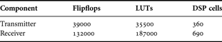
Table 4 shows the resource usage for the transmitter and receiver digital baseband processor. One LUT is a lookup table with six inputs. DSP corresponds to the FPGA-internal digital signal processor hard macros including a 25 × 18 bit multiplier, followed by an adder circuitry. The given numbers correspond to around 100 million logic gates in a standard CMOS technology. In a 40 nm process, the digital baseband processor would thus require a cell area of around 36 mm2.
Table 4. Resource usage of VHR-E synthesized/routed digital baseband.
A full integration of the AFE and digital baseband is not yet possible with such a small structure size. A larger structure size will, however, significantly increase the required cell area of the digital baseband and therefore decrease the production yield.
III. ULTRA-HIGH-RATE POINT-TO-POINT LINKS (UHR-C)
A) Transceiver architecture
The system concept considered for the prototype implementation of ultra-high-rate point-to-point links (UHR-C) is based on a hybrid implementation of the AFE and digital baseband processing. Aiming for a marketable solution, the component design has, however, been geared towards a single-chip solution that accounts for the following design constraints: low power consumption, small form factor, and low manufacturing costs.
The main challenge for the design and implementation of a wireless system that achieves up to 10 Gbit/s is the lack of suitable data converters (ADCs as well as DACs). State-of-the-art technologies still barely allow for high-resolution data conversion in the GHz range with sufficiently low power consumption [Reference Walden19–Reference Murmann21]. Commercially available high-speed single-chip data converters like the ADC083000 [22] and the EV8AQ160 [23] provide a resolution of 8 bits at sampling frequencies ranging from 2.0 to 5.0 GHz, but come with a power dissipation of up to 5 W. Such a high-power dissipation together with the high costs (up to several k€ per device) make high-resolution data conversion not only unattractive but even impossible for ultra-high-rate point-to-point links that are intended for handheld applications.
The proposed transceiver architecture (see Fig. 7) uses 1-bit data converters with symbol-rate sampling in the GHz range to minimize the power dissipation and manufacturing costs while still exploiting the large bandwidth of the 60 GHz frequency band. Note that, a resolution of 1 bit does not only lower the power dissipation of the data converters, but also makes a gain control at the receiver redundant, which in turn reduces the power dissipation.

Fig. 7. UHR-C transceiver architecture.
When limited to a resolution of 1 bit and symbol-rate sampling, an all-digital implementation of the baseband processing at the transmitter and receiver is not feasible. Parts of the typically digital baseband processing have to be done in the analog domain. This includes the pulse shaping at the transmitter (to satisfy the spectral mask), as well as the filtering and the frequency, phase and symbol clock synchronization at the receiver.
The UHR-C physical layer design, which is introduced in the next section, is based on single-carrier modulation and completely tailored to a transceiver with 1-bit data converters and symbol-rate sampling. Polarization multiplexing (vertical, horizontal) is used to maximize the spectral efficiency in LOS environments. The AFE of the transmitter uses a homodyne implementation, whereas the AFE of the receiver has a heterodyne structure with analog carrier recovery at an intermediate-frequency of 5 GHz and synchronous down-conversion to baseband, as proposed in [Reference Ulusoy, Liu, Peter, Felbecker, Abdine and Schumacher24]. SiGe BiCMOS technology is considered for both the transmitter and receiver AFEs.
B) Physical layer parameters
The UHR-C physical layer has been designed for ultra-high rate handheld applications with a strong LOS path between transmitter and receiver, and a transmission range of up to 1 m (data kiosk scenario). The design can be applied to other applications with low-frequency selectivity of the wireless channel, as well, such as the CT scenario.
The design follows the classical formatting for burst-oriented protocols, where each frame consists of a preamble and a payload part. Since the radio channel is assumed to be largely frequency flat, the use of sophisticated channel equalization techniques is not necessary and pilots for channel estimation are not needed. Channel estimation/equalization is rather impossible anyways with 1-bit data conversion and symbol rate sampling.
Following the concept of 1-bit data conversion, single-carrier differential quaternary phase shift keying (DQPSK) modulation is used. The differential modulation enables frequency flat phase equalization at the receiver when using the analog carrier recovery proposed in [Reference Ulusoy, Liu, Peter, Felbecker, Abdine and Schumacher24]. The residual phase ambiguity of multiples of 90° can be easily resolved in the digital domain.
The bandwidth agrees with most of the worldwide regulations of the 60 GHz frequency band. It follows the IEEE 802.15.3c and ECMA-387 channelization plan [1, 2]. Bonding of two channels is used to obtain a total bandwidth of 4.32 GHz at 61.56 GHz carrier frequency. Allowing for a guard band of 20% that accounts for the slopes of convenient pulse shaping filters, the symbol rate follows as 3.456 GHz. The separation between downlink and uplink relies on a time division duplex scheme that is part of the MAC layer.
The physical layer comprises four configurations with different data rates that derive from two different code rates (1/2 and 3/4) and the usage of polarization multiplexing. The parameters and data rates of the four configurations are given in Table 5.
Table 5. UHR-C physical layer parameters.

The design involves a massive data parallelization to allow for digital baseband processing at a clock rate of only 108 MHz. Three types of parallelism are jointly used to match the ultra-high data rates to such a low processing speed: (1) Vertical polarization and horizontal polarization carry independent data frames in parallel (when in use). (2) For each polarization, two parallel data frames are transmitted using inphase and quadrature phase of the DQPSK symbols separately. (3) The payload of each frame is split into five serial sequences of 32 parallel code words of length 1024 each. This leads to 64- and 128-fold parallelization for the single-input single-output (SISO)-A/B and multiple-input multiple-output (MIMO)-A/B configurations (see Table 5), respectively. The MIMO-A/B configurations double the data rate of SISO-A/B by exploiting vertical and horizontal polarization with negligible crosstalk.
The preamble has the same structure for all configurations. It contains an analog training part that is used for symbol clock recovery and is a sequence of alternating “0” and “1” in each parallel frame. The digital training part is an M-sequence of length 1023 + 1, which is different for each parallel frame. It is used for packet detection and for resolving phase ambiguities of multiples of 90°. The signaling field carries MAC layer information and contains 32 information bits that are encoded with a spreading sequence of length 32. This length allows en-/decoding of one information bit at one clock cycle of 108 MHz.
The convolutional coding used for the payload is based on a mother code of rate 1/3 with termination and puncturing as given in [Reference Proakis15] to deliver the two code rates 1/2 and 3/4.
C) Link-budget analysis
This section considers the link budget for the UHR-C physical layer configurations introduced above. Table 6 summarizes the parameters. They are very similar to those used for VHR-E. Following the cost requirements for handheld devices, only the SiGe figures have been considered for the PA performance and the receiver noise figure. An average transmit power of 9 dBm has been assumed, which is a rather conservative assumption for single-carrier QPSK. The parameters of the path loss exponent model are very close to the values for free space propagation. They have been extracted from channel measurements for the data kiosk scenario [Reference Garcia11]. A shadowing margin is not taken into account, as only LOS transmission is considered. A 3 dB margin has been considered instead that accounts for losses induced by polarization mismatch and misalignment, which are relevant for the data kiosk scenario.
Table 6. UHR-C link budget parameters.

For the CT scenario, the coupling between transmitter and receiver is achieved via a rotating dielectric image line. Again, the channel gain is used (see Section II.C) to emphasize that antenna gains and the path loss model do not apply in this case. The minimum channel gain for this setup is −30 dB including propagation and coupling losses. Polarization multiplexing is not feasible for the CT scenario.
The link-budget results are given in Table 7. They reveal that the SISO-B configuration is feasible for a distance of up to a 3.1 m and that SISO-A configuration has an operational range of even 3.9 m. Even when assuming that polarization crosstalk does not constrain the performance, the ranges reduce for the MIMO-A/B configuration. This is due to the fact that the transmit power is divided among two TX branches. (Note that the thermal noise power for MIMO-A/B in Table 7 applies to each RX branch.) However, regarding the target range of 1 m, there are still operational margins of 8.6 and 6.8 dB, respectively. Margins beyond 33 dB arise for the CT scenario, so that a data rate of 5 Gbit/s can be easily supported. Thus, there is room for either reducing the transmit power, considering larger coverage, or even increasing the data rate in future. The latter may be achieved by extending the bandwidth or, when not restricted to 1-bit data converters, by using higher-order modulation schemes.
Table 7. UHR-C link budget results.

D) Link-level simulations
In addition to the link-budget analysis, MATLAB-based link-level simulations have been done to evaluate the expected UHR-C physical layer performance with detailed AFE models and measured 60 GHz channel characteristics for the data kiosk scenario. The simulation chain comprises the complete digital baseband processing (including the frame formatting, DQPSK modulation, preamble-based synchronization, convolutional encoding, Viterbi decoding, etc.) and therefore also serves as a reference for the hardware implementation described in Section III.E. The simulation chain further models the AFEs of the transmitter and receiver and the 60 GHz radio channel as described below.
1) AFE and channel models
Equivalent baseband models have been used to model the behavior of the AFEs, and the frequency selectivity of the measured 60 GHz channel. The parameterization of the AFE models follows from data sheets and from specifications of the analog components that have been designed and implemented in the EASY-A project.
For the pulse shaping and filtering at the transmitter and receiver, commercially available analog filters are considered, i.e., VLF1870 and SBLP1870 from MiniCircuits. The VLF1870 serves as a pulse shaping filter to satisfy the spectral mask following the ECMA-387 standard [2]. The impulse responses of the filters can be computed from the S-parameters available from the MiniCircuits website [25]. Ideal root-raised-cosine (RRC) filters with roll-off factor 0.3 have been considered for comparison.
The 60 GHz up-conversion at the transmitter is subject to I/Q imbalance and phase noise, which are modeled in baseband according to [Reference Schenk and Linnartz26, Reference Bittner, Krone and Fettweis27]. A gain imbalance of 1 dB and a phase imbalance of 10° have been considered. The phase noise model assumes a second-order PLL with a voltage controlled oscillator (VCO) that has a phase noise of −90 dBc/Hz at 1 MHz, a reference oscillator that has a phase noise of −130 dBc/Hz at 1 kHz, a loop filter bandwidth of 4 MHz, and a cut-off frequency of the phase noise spectrum of 441 kHz. This parameterization delivers the same phase noise spectrum as the actual analog hardware design.
The non-linearity of the transmit PA is modeled according to Rapp's solid-state-amplifier model [Reference Rapp28], which is given by |y| = g(|x|) = (1 + [|x|2/P max]p)−1/2p, where |x| and |y| denote the input and output signal amplitudes. The model parameters are p = 2.15 and P max = 15 dBm. The average transmit power and the transmit antenna gain are 9 dBm and 9 dBi, as considered in the link budget.
The 60 GHz radio channel has been simulated using baseband channel impulse responses that have been obtained from measurements [Reference Garcia11] and reflect the path loss, the frequency selectivity, and the polarization crosstalk characteristics. Two distances been considered: 0.5 and 1.0 m.
The receive antenna gain and the receiver noise figure are 9 dBi and 10 dB, as considered in the link budget. A Butterworth filter of second order with 3 dB bandwidth of 3.456 GHz accounts for the limited bandwidth of the transmit and receive antennas.
The phase noise of the 60 GHz down-conversion stage at the receiver is modeled according to [Reference Bittner, Krone and Fettweis27], assuming a free-running VCO that has a phase noise of −90 dBc/Hz at 1 MHz. The model for the synchronous down-conversion with analog carrier recovery at 5 GHz follows the structure proposed in [Reference Ulusoy, Liu, Peter, Felbecker, Abdine and Schumacher24], considering a Butterworth bandpass filter of fourth order with a 3 dB bandwidth of 150 MHz. The receiver I/Q imbalance at the output of the 5 GHz stage has been modeled according to [Reference Schenk and Linnartz26] with a gain imbalance of 1 dB and a phase imbalance of 5°.
2) Simulation results
The physical layer performance is evaluated in terms of different error rates, i.e., bit error rate of the payload (BER), code word error rate of the payload (CWER), bit error rate of the signaling field (SFER), and missed detection rate (MDR) which accounts for lost frames. A missed detection is declared if one or more bits of the signaling field are wrong.
Table 8 shows the simulation results for the four physical layer configurations. Ideal timing (symbol clock) synchronization between transmitter and receiver has been assumed for all simulations.
Table 8. Simulation results for the UHR-C physical layer.

The results indicate that the MDR and the SFER performance are satisfactory in all cases, which is due to the long digital training sequence and the low code rate of the signaling field. For the configurations that only use a single polarization (SISO-A/B), a reasonable BER and CWER performance can be achieved even with commercially available baseband filters and significant AFE impairments. The results obtained for the configurations that use two polarizations (MIMO-A/B), however, indicate that the polarization crosstalk of the channel together with the inter-symbol interference caused by non-ideal baseband filters, lead to rather high error rates that will not allow for the anticipated throughput of up to 10 Gbit/s. A data rate of 10 Gbit/s can, however, be achieved when the system is not restricted to commercially available baseband filters, but when dedicated transmit and receive filters with flat group delay (such as RRC-like matched filters) can be implemented.
E) Digital baseband implementation
An FPGA-based platform from The Dini Group [29] has been used for the hardware implementation of the UHR-C digital baseband. For each UHR-C transceiver, the platform consists of a DN7006K10PCIe-8T board with six Altera Stratix III (3SL340) FPGAs and is extended by two DNMEG_2SGX daughter-cards with one Altera Stratix II GX FPGA each. The multi-gigabit transceivers of the Stratix II GX devices serve as the 1-bit data converters interfacing the AFE. They are used in basic mode (without any specific protocol) at a data rate of 3.456 Gbit/s. Newer Altera Stratix V GT devices even allow up to 28 Gbit/s [30]. Two multi-gigabit transceivers are used for the digital baseband implementation of the SISO-A/B configuration, whereas four multi-gigabit transceivers are required for the MIMO-A/B configuration. Each multi-gigabit transceiver has an integrated analog clock recovery unit (CRU) that is used for the symbol clock recovery at the receiver side.
The hardware implementation has been divided into data paths for the transmitter and receiver (each with a dedicated controller), a MAC layer interface, and a system-on-chip (SoC) module that serves as an overall controller of the digital baseband with an interface to a host PC.
The implementation of the transmitter and receiver data paths is based on a linear data flow structure as described below. Both data paths are clocked at 108 MHz.
1) Transmitter data path
Figure 8 shows the block diagram of the transmitter data path for the SISO-A/B configuration. The MIMO-A/B configuration requires two of these data paths in parallel.

Fig. 8. UHR-C transmitter data path (SISO-A/B configuration).
The SISO input module splits the 64-bit data words coming from the MAC interface into two 32-bit words that are fed into the processing chains of the inphase and quadrature phase. The convolutional encoder modules perform the encoding with rate 1/3 and termination. Each encoder module consists of 32 encoders that are fed by 32 independent data bits in parallel. The puncturing and the differential modulation have been realized as a single module. The two 96-bit words coming from the encoders are de-multiplexed according to the puncturing pattern and fed into a FIFO. The FIFO is read by a differential modulation unit, which joins the in-phase and quadrature-phase sequences according to the differential modulation scheme. It consists of four parallel modulators that account for the four possible DQPSK symbol states and a subsequent logic that selects the 32 output bits according to the actual states at each 108 MHz clock cycle. The framing module adds the preambles in front of the payload of each frame. This includes the encoding of the signaling field data bits, which are generated by the controller of the transmitter data path (not depicted in Fig. 8). At each clock cycle, 32 output bits are then fed into each of the two multi-gigabit transceivers, which perform a 32-fold serialization to deliver in-phase and quadrature-phase output symbols at a rate of 3.456 GHz.
2) Receiver data path
The receiver data path realizes complementary functionality to the transmitter data path. Figure 9 shows the block diagram of the receiver data for the SISO-A/B configuration. The MIMO-A/B configuration requires again two of these data paths in parallel.

Fig. 9. UHR-C receiver data path (SISO-A/B configuration).
The in-phase and quadrature-phase symbols (bits) coming from the analog receiver frontend are de-serialized with two multi-gigabit transceivers, each of which delivers 32-bit words at a rate of 108 MHz. The clock synchronization between transmitter and receiver is done by the FPGA-integrated CRU of the multi-gigabit transceivers. The received 32-bit words of the inphase and quadrature phase are jointly fed into an acquisition module that performs packet detection, phase, and timing synchronization. The acquisition module consists of four parallel cross-correlation units that correlate the received bits with phase-shifted versions of the digital training sequences to resolve phase ambiguities of multiples of 90°, a threshold detector and a multiplexer. Each cross-correlation unit comprises 32 parallel cross-correlators (shifted by 0–31 bits) to detect the correct timing instant within the 32-bit input words. Hence, there are 128 cross-correlators operating in parallel. Once one of the cross-correlators exceeds a threshold, a frame is received. The received bits are then multiplexed and delayed in such a way that the two 32-bit output words at each clock cycle match the parallel structure of the transmitter, i.e., the 128 possible combinations of phase and time shifts are compensated by this multiplexing. The differential demodulation and depuncturing have been realized as a single module, in the same manner as the puncturing and modulation at the transmitter. The Viterbi decoder modules decode the received bits with the code rate 1/3. Each decoder module consists of 32 Viterbi decoders and outputs 32 independent data bits in parallel. The SISO ouput module combines the two 32-bit data words coming from the receiver processing chains of the inphase and quadrature phase to 64-bit data words, which are then fed into the MAC interface of the receiver.
3) System on chip
A SoC module connects the transmitter and receiver data paths to a host PC that controls and monitors the digital baseband (with dedicated control registers), and allows to write/read data to/from the data paths via an Ethernet connection (without using the MAC interface). Since the Ethernet connection has a limited data rate of 70 Mbit/s, on-board DDR2 memory with high access rate is used to cash the data. This cashing further allows the computation of performance measures, such as the BER, from the data that has been transmitted and received. The BER calculation is part of the SoC and has been realized as a DDR2 memory-based comparison of the received data with the transmitted data which is stored as reference in one memory part.
4) FPGA mapping and resource usage
Figure 10 illustrates the mapping of the digital baseband modules to the FPGAs of one hardware platform, and the required interfaces. FPGAs “Tx” and “Rx” denote the Altera Stratix II GX devices on the DNMEG_2SGX daughter cards that connect to the AFEs. FPGAs “A” to “D” denote the Altera Stratix III devices on the DN7006K10PCIe-8T mother board, which are used for the digital baseband processing. The receiver data path for the SISO-A/B configuration fits on one Altera Stratix III FPGA, whereas two Altera Stratix III FPGAs are required to implement two parallel data paths for the MIMO-A/B configuration. The reason is the relatively large size of the acquisition module and the Viterbi decoders.

Fig. 10. FPGA mapping of the UHR-C digital baseband (SISO-A/B configuration).
Table 9 shows the resource usage of the transmitter and receiver data paths (including the respective controllers) and of the SoC module for the SISO-A/B configuration (FPGA “A” is not used). The first column refers to the logic usage, whereas the other columns refer to the memory usage. An ALUT is an adaptive lookup table with four to six inputs. The high logic and memory usage of the receiver data path is mainly due to the size of the acquisition module with 128 parallel cross-correlators and the Viterbi decoding modules with 64 parallel Viterbi decoders.
Table 9. Resource usage of UHR-C synthesized/routed digital baseband.

IV. CONCLUSIONS
This paper has addressed the application-specific physical layer design, link budgets, simulation results, and digital baseband implementation for very-high rate point-to-multipoint links (VHR-E) and ultra-high rate point-to-point links (UHR-C) at 60 GHz. Although the VHR-E physical layer design is based on OFDM, the UHR-C design relies on DQPSK single-carrier modulation with massive parallelization.
The link-budget analysis for VHR-E has revealed that a data rate of 1.3 Gbit/s is feasible at a distance of up to 9.7 m and a data rate of 2.6 Gbit/s at a distance of up to 4.5 m in the CDL scenario, when using SiGe technology. For the STR case with dynamic shadowing, the range reduces to 3.5 m when requiring a link reliability of 90%. With GaAs technology, the target range of 10 m is feasible for the CDL as well as the STR scenario. This justifies the usage of both technologies. Despite the high losses due to severe shadowing in the in-car entertainment scenario, a data rate of 1.3 Gbit/s can be supported with GaAs. Even twice this rate is tightly feasible.
For the LOS-dominated UHR-C system, the target range of 1 m is easily exceeded, or large operational margins arise at the target range, respectively. This lowers the requirements on hardware accuracy and implies optimal conditions for the use of low-cost frontend technology. The link-level simulation results indicate, however, that the polarization crosstalk together with the inter-symbol interference caused by non-ideal baseband filters can still significantly degrade the system performance. A dedicated baseband filter design with flat group delay is required.
The digital baseband implementations for the VHR-E and UHR-C prototypes are currently being finalized and are expected to soon allow for the demonstration of real-time data transmission at 60 GHz. A data rate of 2.6 Gbit/s over a distance of 2 m has recently been demonstrated for VHR-E, using an emulated receiver with a sample-and-store hardware and offline demodulation.
ACKNOWLEDGEMENTS
This work has been supported by the German Federal Ministry of Education and Research (BMBF) under grants 01BU0800 to 01BU0815. The authors acknowledge the excellent cooperation with all project partners in the EASY-A project, and the valuable contributions of Marco Krondorf, Steffen Bittner and Hermann Hensel, who have been involved in the implementation of the UHR-C digital baseband at TU Dresden, Germany.
 Stefan Krone received his Dipl.-Ing. (MSEE) from TU Dresden, Germany, in 2007. From 2001 to 2006 he was research assistant at Fraunhofer IPMS in Dresden and Fraunhofer IIS in Erlangen, Germany. Since 2007, he is research associate at the Vodafone Chair Mobile Communications Systems at TU Dresden, working towards his Ph.D. In 2010, he was research visitor at the University of California in Santa Barbara, USA. His research interests include physical layer design for ultra-wideband communications, signal processing with low-resolution data conversion, and information theory.
 Falko Guderian received his M.S. in Business Informatics and M.S. in Industrial Engineering and Management from TU Dresden, Germany, in 2006 and 2007, respectively. Thereafter he was automation engineer for mask data processing at Advanced Mask Technology Center Dresden, Germany, a joint venture of Globalfoundries and Toppan Photomasks. Since 2008, he is research associate at the Vodafone Chair Mobile Communications Systems at TU Dresden, Germany. His research interests include rapid prototyping in digital signal processing and design space exploration of multi/many-core systems.
 Gerhard Fettweis earned his Ph.D. from RWTH Aachen, Germany, in 1990. Thereafter he was visiting scientist at IBM Research in San Jose, USA, and scientist at TCSI Inc., Berkeley, USA. Since 1994 he is Vodafone Chair Professor at TU Dresden, Germany, with currently 20 companies from Asia/Europe/USA sponsoring his research on wireless communications and chip design. He has spun-out nine start-ups in Dresden, so far. He is IEEE Fellow, and has received many awards. He has been actively involved in organizing IEEE conferences, most notably being TPC Chair of the IEEE ICC 2009 in Dresden, Germany.
 Markus Petri received his Dipl.-Ing. (MSEE) from TU Berlin, Germany, in 2006. Afterwards, he was active in the field of vision sensors and vision components for industrial automation, where he developed an optical particle sensor for mass spectrography, a 3D-TOF-system and high-speed digital cameras. He is now with IHP Microelectronics in Frankfurt (Oder), Germany. His research interests include digital systems for ultra-high data rates and systems concepts for future wireless broadband communications. Markus Petri received the Erwin-Stephan-Price in 2008 and was an e-fellows.net stipendiary from 2004 to 2006.
 Maxim Piz received his Dipl.-Ing. (MSEE) from the TU Berlin, Germany, in 2003. He has been working as a researcher and developer in the area of 60 GHz broadband wireless communications at IHP Microelectronics in Frankfurt (Oder), Germany, from December 2003 to September 2010, where he contributed to the baseband design for the BMBF-funded projects WIGWAM and EASY-A, both at simulation and implementation level. Based on this work, he submitted a Ph.D. thesis.
 Miroslav Marinkovic received his Dipl.-Ing. and the MSEE from the University of Nis, Serbia, in 2004 and 2008, respectively. Since 2008 he is with IHP Microelectronics in Frankfurt (Oder), Germany, as a research associate. His research activities focus on digital signal processing for high-speed wireless communications and error control coding.
 Michael Peter received his Dipl.-Ing. (MSEE) from University of Karlsruhe, Germany, in 2004. In 2005, he joined the Fraunhofer Heinrich Hertz Institute in Berlin, Germany. His research activities focus on 60 GHz communication, wideband channel modeling, and physical layer design of wireless broadband communication systems.
 Robert Felbecker received his Dipl.-Ing. (MSEE) from the RWTH Aachen University, Germany, in 2007. Since 2007, he is with the Fraunhofer Heinrich Hertz Institute in Berlin, Germany. He is involved in the fields of measurement and simulation of electromagnetic wave propagation.
 Wilhelm Keusgen received his Dipl.-Ing. (MSEE) and Dr.-Ing. (Ph.D.) from RWTH Aachen, Germany, in 1999 and 2005, respectively. From 1999 to 2004, he was with the Institute of High Frequency Technology at RWTH Aachen University, where he worked on multiple antenna systems, microwave frontend technologies, and microwave antennas. In 2004, he joined the Fraunhofer Heinrich Hertz Institute in Berlin, Germany. There, he leads a research group, which is focused on the design and implementation of broadband mobile communication systems. His main research areas are millimeter-wave communication, car-to-car communication, and digital compensation of RF impairments especially for power amplifiers.


