


Introduction
Now-a-days, single antenna is desired for more than one application. Many researchers have made large efforts to design such kind of antennas, which can be used for multiband operations [Reference Fusco1–Reference Singh3]. Several researchers have worked in the field of multiband antennas [Reference Khandelwal4]. Small frequency ratios between two consecutive resonant frequencies are a great challenge to achieve while designing a multiband antenna [Reference Nasimuddin, Chen and Xianming5, Reference Bao and Ammann6]. In the same regard, several types of antenna structures with small frequency ratio have been designed for different wireless applications [Reference Kumar7–Reference Ansari10]. Directional wide-band antenna with asymmetric fed has been presented in order to optimize antenna gain [Reference Thomas and Sreenivasan11, Reference Ammann and Chen12]. A printed parasitic element with metamaterial also has been embedded with a wide-band antenna for desired multiband operation [Reference Tong13–Reference Siddiqui16]. Wide impedance bandwidth also has been achieved with multiband operation by using slotted antenna [Reference Chen and Yung17–Reference Wang19]; however, reported antennas are based on multiple feeding networks, which introduce some deficiencies in the performance including mutual coupling and spurious radiations from feed. As the recent requirement for commercial communication applications, multiband antennas should be operated in non-direct line of sight (NLOS), wireless Internet service providers (WISP), C-band application such as weather radar systems (3.7–4.2 GHz), Mobile-WiMAX (2.5/3.3/3.5 GHz), and higher WLAN (5.05–5.35 GHz) [Reference Khanam9–Reference Aguilar23].
In this article, a penta-resonant, novel-shaped patch antenna along with dipole and metamaterial is proposed with very small frequency ratio. Design steps are presented and discussed along with its performance parameters. The proposed design characteristics are analyzed using Ansoft HFSS v.15 based on finite element method and results are matched with the measurement of fabricated antenna's prototypes. The proposed antenna is low profile and fabricated on an FR-4 Epoxy substrate, which is cheaper and commercially available. It can be easily fabricated on a single substrate using standard photolithography process, which is a merit of the proposed antenna over available literature.
Proposed structure
The schematic representation and design steps of the proposed structure are presented in Figs 1 and 2. An equilateral triangular patch of edge S is taken as a reference in Fig. 1(a). This equilateral triangular patch is fed by a microstrip line of length L ml and width W ml. The input impedance of the patch is matched with the characteristics impedance of microstrip line through inset feed of length y 0 and slot width w 0. The structure is designed for 5 GHz and detailed parameters are given in Table 1.
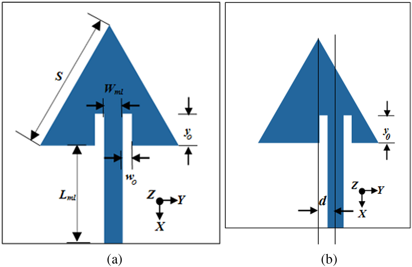
Fig. 1. Schematic representation of the triangular patch antenna with (a) inset feed and (b) asymmetric offset inset feed.

Fig. 2. Schematic representation and step-by-step evolution of the proposed design; (a) case I – Ant_1, (b) case II – Ant_2, (c) case III – Ant_3, (d) case IV – Ant_4, and (e) case V – Ant_5.
Table 1. Design specification of antenna designs along with their metamaterials

Length L ml of the microstrip line is calculated as [Reference Kumar and Ray24, Reference Balanis25]
 $$L_{ml} = \displaystyle{c \over {4f_r\sqrt {\varepsilon _{effml}}}}, $$
where
 $$\; \varepsilon _{effml} = \displaystyle{{\varepsilon _r + 1} \over 2} + \displaystyle{{0.5(\varepsilon _r - 1)} \over {\sqrt {1 + 12(h/W_{ml})}}}, $$
 $$S = S_{eff} - \displaystyle{{4h} \over {\sqrt {\varepsilon _r}}}, $$
where S, S eff, h, and ε r are the edge of the equilateral triangular patch, the effective length of the edge of the equilateral triangular patch, height of the dielectric substrate, and relative dielectric constant of the dielectric substrate, respectively.
Effective length S eff is calculated as [Reference Balanis25]
 $$S_{eff} = \displaystyle{{2C} \over {3f_r\sqrt {\varepsilon _{eff}}}}, $$
where C, ε eff, and f r are the speed of light in free space, effective dielectric constant, and resonance frequency, respectively.
Further, the asymmetric feed is introduced in the equilateral triangular patch as shown in Fig. 1(b). The microstrip line is shifted toward its right by a distance d for asymmetric feed. Offset feed method for triangular patch antenna has been reported for the enhancement of impedance bandwidth [Reference Thomas and Sreenivasan11, Reference Ammann and Chen12]. Asymmetric feed provides directional radiation in the end-fire direction (z-direction) as shown in Fig. 3. It is observed that antenna starts to radiate in the end-fire direction as the offset distance d is increased to the value of S/4.

Fig. 3. The radiation pattern of a triangular patch antenna for different values of offset distance d; (a) E-plane, (b) H-plane.
The schematic representation and step-by-step evolution of the proposed structure are shown in Fig. 2. In case I, offset feeding is introduced in the equilateral triangular patch to achieve the directional radiation pattern and the antenna structure is referred as Ant_1, which is shown in Fig. 1(b).
For case II, a dipole is designed for 2.5 GHz and embedded with a triangular patch, which is referred as Ant_2 and shown in Fig. 2(b). Half-length of the dipole is embedded with a patch on the signal plane, whereas a slot of length (Ln 1 + x 1) is embedded on the ground plane; in which, x 1 is the width of the connecting strip. The length L n1 and width W n1 of the first dipole are calculated from equations (5) and (6), respectively.
Half-length L n/2 of the dipole is the quarter wavelength and calculated as
 $$\displaystyle{{L_n} \over 2} = \displaystyle{{\lambda _{eff}} \over 4} = \displaystyle{c \over {4f_r\sqrt {\varepsilon _{eff}}}}, $$
where c, ε eff, and f r are the speed of light in free space, effective permittivity (εeff ≤ εr), and resonating frequency of dipole, respectively. Resonant frequency f r of the dipole is taken as 2.5 GHz in this study.
Width W n1 of the dipole corresponding to its length L n1 is related to its impedance and calculated by equation (6) [Reference Balanis25]. The impedance of the dipole is matched to the input impedance of the edge of the microstrip patch.
 $$W_n = \displaystyle{{\pi L_n} \over {exp((R_{in}(x = 0)/120) + 2.25)}},$$
where R in (x = 0) is the input impedance at the edge of microstrip patch antenna and calculated by equation (7) [Reference Kumar and Ray24]:
 $$R_{in}(x = 0) = \displaystyle{{50} \over {cos^2(\pi S_0/S)}},$$
where S is the edge of the equilateral triangular patch and S 0 is the length of the transmission line corresponding to 50 Ω impedance.
In case III, one more dipole is embedded and the structure is referred as Ant_3, which is shown in Fig. 2(c). The second dipole is designed for 4 GHz, and the length L n2 and width W n2 are calculated by equations (5) and (6), respectively. Their relevant values are adjusted up to the minimum extent to maintain the resonant peak at the specific frequency by parametric analysis.
In case IV, an inter digital capacitor-loaded loop resonator (IDCLLR) [Reference Tong13, Reference Peng and Zhang14] is embedded below the right corner of the edge of the triangular patch as shown in Fig. 2(d) and the structure is referred as Ant_4.
In case V, a slot and a slit of rectangular split-ring resonators (SRR) [Reference Lin and Cui15, Reference Siddiqui16] are embedded in the left corner of the triangular patch as shown in Fig. 2(e) and the structure is referred as Ant_5. The top and bottom views of a schematic representation of the proposed Ant_5 (case V) are shown in Figs 4(a) and 4(b), respectively. The dimensions of a single unit cell of rectangular SRR and IDCLLR are shown in Fig. 5, and the real permittivity, permeability, and refractive index of the unit cell are shown in Figs 6(a) and 6(b). The detailed dimensions of all the structures are listed in Table 1.

Fig. 4. Schematic representation of the proposed design Ant_5; (a) top view, (b) ground plane, (c) side view, and (d) fabricated prototype.

Fig. 5. Schematic representation of a single unit; (a) rectangle SRR, (b) IDCLLR.

Fig. 6. Metamaterial characteristic of a single unit; (a) rectangular SRR, (b) IDCLLR.
Analysis and result discussion
The FR-4 Epoxy substrate of dimensions 35 mm × 35 mm × 1.5748 mm is used to analyze the proposed antennas. Fabrication is done by standard photolithography process and measurement is done by Agilent™PNA-L Series Network Analyzer and Agilent™ Spectrum Analyzer. A fabricated prototype of Ant_5 is depicted in Fig. 4(d). Figure 7 shows the S 11 variation with the frequencies Ant_1, Ant_2, Ant_3, and Ant_4 corresponding to cases I–IV. Ant_5 shows five resonating frequency bands with very small frequency ratios as shown in Fig. 8. S 11 and VSWR characteristics with the frequency of Ant_5 is shown in Figs 8(a) and 8(b), respectively. All five resonating bands are achieved by the presented mathematical design equations; however, the least parametric analysis is done to achieve sharp resonance for the specific applications. Ant_5 resonates at 2.58, 3.17, 3.42, 4.0, and 5.3 GHz with very small frequency ratios of the values 1.2286, 1.078, 1.169, and 1.325 between two consecutive resonant frequencies, respectively. A comparative study is shown in Table 2.

Fig. 7. S 11 characteristics with the frequency of Ant_1, Ant_2, Ant_3, and Ant_4.

Fig. 8. Measured and simulated characteristics with the frequency of the proposed antenna Ant_5; (a) S 11, (b) VSWR.
Table 2. Frequency ratio of the proposed design Ant_5 in comparison with recent works

The current distribution of the proposed antenna Ant_5 at each resonant frequency is shown in Fig. 9. The working mechanism of the proposed antenna could be defined with the help of the shown current distribution: (i) dipoles embedded in the front of the triangular patch and ground are mainly contributing to generate 2.58 GHz frequency as shown in Fig. 9(a); (ii) 3.17 GHz frequency is achieved due to a slot and a slit of rectangular SRR, which can be clearly observed in Fig. 9(b); (iii) IDCLLR combined with a slit and a slot are playing a role in generating 3.42 GHz frequency; and finally (iv) 4 and 5.3 GHz frequencies are achieved due to the triangular patch with inset feed as shown in Figs 9(d) and 9(e), respectively.

Fig. 9. Current distributions at (a) 2.58 GHz, (b) 3.17 GHz, (c) 3.42 GHz, (d) 4 GHz, and(e) 5.3 GHz.
Radiation patterns of the proposed antenna Ant_5 are shown in Fig. 10. E-plane patterns of Ant_5 are shown in Figs 10(a), 10(c), 10(e), 10(g), and 10(i); whereas H-plane patterns are shown in Figs 10(b), 10(d), 10(f), 10(h), and 10(j) at 2.58, 3.17, 3.42, 4.0, and 5.3 GHz frequencies, respectively. It is observed from Fig. 10 that Ant_5 shows good radiation characteristics in both major planes. Measured results are in good agreement with the simulated results.

Fig. 10a. Measured and simulated normalized radiation pattern of the proposed antenna; (a) E-plane at 2.58 GHz, (b) H-plane at 2.58 GHz, (c) E-plane at 3.17 GHz, (d) H-plane at 3.17 GHz, (e) E-plane at 3.42 GHz, (f) H-plane at 3.42 GHz, (g) E-plane at 4 GHz, (h) H-plane at 4 GHz, (i) E-plane at 5.3 GHz, and (j) H-plane at 5.3 GHz.

Fig. 10b. Continued.
Figure 11 shows the measured gain variation with the frequency of the proposed antenna. Ant_5 shows antenna gain of about 3.23, 2.9, 2.8, 4.01, and 3.49 dBi at frequencies 2.58, 3.17, 3.42, 4, and 5.3 GHz, respectively. Antenna efficiency is shown in Fig. 12, and it is observed that the proposed antenna Ant_5 shows antenna efficiency around 87.5, 83.05, 82.45, 89.35, and 88.93% at respective bands. Performance of proposed Ant_5 is compared in Table 3.
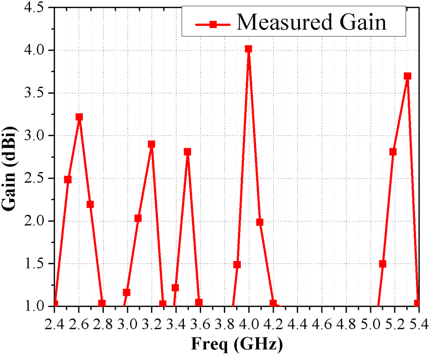
Fig. 11. Measured gain variation with the frequency of the proposed antenna.

Fig. 12. Measured antenna efficiency variation with the frequency of the proposed antenna Ant_5.
Table 3. Performance of the proposed design Ant_5 in comparison with recent works

Conclusion
A novel-shaped penta-resonant antenna is designed and analyzed. The proposed antenna is resonating at 2.58, 3.17, 3.42, 4, and 5.3 GHz with a very small frequency ratio of the values 1.2286, 1.078, 1.169, and 1.325 between two consecutive resonant frequencies, respectively. Simulated results of the designed antenna are verified with measured results of the fabricated antenna. Proposed antenna shows good radiation characteristics and may be used for multiple wireless applications such as 2.58 GHz for NLOS, WISP, and compatible with Navini Networks (2.5–2.690 GHz); 3.17 and 3.42 GHz for WiMAX (3.3/3.7 GHz in Asia); 4 GHz for C-band application such as weather radar systems (3.7–4.2 GHz); and 5.3 GHz for higher WLAN (5.05–5.35 GHz).
 Praveen Chaurasia received his B.E. degree in Electronics and Communication in 2010 from RGPV, Bhopal, India, and M.Tech. degree in Electronics and Communication in 2013 from Malaviya National Institute of Technology, Jaipur, India. Currently, he is pursuing Ph.D. from IIT(ISM), Dhanbad, India. He has published 2 research papers in reputed international journal and conference. His current research interests are on multiband microstrip antenna, microstrip antenna with engineered material like meta-material and microwave components.
 Binod Kumar Kanaujia is currently working as Professor in the School of Computational and Integrative Science, Jawaharlal Nehru University, Delhi-110067, India since 01-Aug-2016. Previously Dr. Kanaujia was working as a Professor in the Department of Electronics & Communication Engineering in Ambedkar Institute of Advanced Communication Technologies & Research (formerly Ambedkar Institute of Technology), Geeta Colony, Delhi from 17-Aug-2012. Dr. Kanaujia joined this institute as Assistant Professor in 2008 through selection by Union Public Service Commission, New Delhi, India and promoted to Associate Professor on 21-Feb-2008. He served on various key portfolios i.e. Head of Department, In-charge Central Library, Head of Office, etc. Before joining this institute, he had served in the M.J.P. Rohilkhand University, Bareilly, India as Reader in the Department of Electronics & Communication Engineering and also as Head of the Department. He has been an active member of Academic Council and Executive Council of the M.J.P. Rohilkhand University and played a vital role in academic reforms. Prior, to his career in academics, Dr. Kanaujia had worked as Executive Engineer in the R&D division of M/s UPTRON India Ltd. Dr. Kanaujia had completed his B.Tech in Electronics Engineering from KNIT Sultanpur, India in 1994. He did his M.Tech and Ph.D. in 1998 and 2004; respectively from Department of Electronics Engineering, Indian Institute of Technology Banaras Hindu University, Varanasi, India. He has been awarded Junior Research Fellowship by UGC Delhi in the year 2001-02 for his outstanding work in the electronics field. He has a keen research interest in design and modeling of the microstrip antenna, dielectric resonator antenna, left-handed metamaterial microstrip antenna, shorted microstrip antenna, ultra-wideband antennas, reconfigurable and circular polarized antenna for wireless communication. He has been credited to publish more than 200 research papers with more than 900 citations with h-index of 15 in peer-reviewed journals and conferences. He had supervised 50 M.Tech and 15 Ph.D. research scholars in the field of microwave engineering. He is a reviewer of several journals of international repute i.e. IET Microwaves, Antennas & Propagation, IEEE Antennas and Wireless Propagation Letters, Wireless Personal Communications, Journal of Electromagnetic Wave and Application, Indian Journal of Radio and Space Physics, IETE Technical Review, International Journal of Electronics, International Journal of Engineering Science, IEEE Transactions on Antennas and Propagation, AEU-International Journal of Electronics and Communication, International Journal of Microwave and Wireless Technologies, etc. Dr. Kanaujia had successfully executed 04 research projects sponsored by several agencies of Government of India i.e. DRDO, DST, AICTE and ISRO. He is also a member of several academic and professional bodies i.e. IEEE, Institution of Engineers (India), Indian Society for Technical Education and The Institute of Electronics and Telecommunication Engineers of India.
 Santanu Dwari was born in Howrah, West Bengal, India. He received his B.Tech and M.Tech degree in Radio Physics and Electronics from University of Calcutta, Kolkata, West Bengal, India in the year of 2000 and 2002 respectively and Ph.D. degree from Indian Institute of Technology, Kharagpur, West Bengal, India in the year of 2009. He joined Indian School of Mines, Dhanbad, Jharkhand, India in 2008 where he is currently an Assistant Professor in the Department of Electronics Engineering. He has published seven research papers in referred International Journals. He is carrying out two sponsored research projects as Principal Investigator. His research interest includes Antennas, RF planar circuits, Computational Electromagnetics.
 Mukesh Kumar Khandelwal was born in Uttar Pradesh, India and received his B.Tech. degree in Electronics & Communication Engineering, M.Tech degree in Digital Communication from GGSIP University, Delhi, India and Ph.D Degree in Electronics Engineering from Indian Institute of Technology ISM, Dhanbad, India. Dr. Khandelwal is working as an Associate Professor in the Department of Electronics & Communication Engineering, Bhagwan Parshuram Institute of Technology, Delhi India which is affiliated to Guru Gobind Singh Indraprastha University Delhi India (Govt of NCT Delhi, India). He has published Twenty Five research papers in referred International Journals. Dr. Khandelwal is serving as a reviewer in various renowned journals i.e. IEEE MTTs (USA), IEEE Access (USA), IET Microwave Antenna and Propagation(UK), IET Electronics Letters (UK), Wireless Personal Communication (Springer, Netherland), International Journal of Electronics and Communications, (Elsevier), Journal of Electromagnetic Waves and Applications, Taylor & Francis (UK) etc. His current research interests focus on microstrip antennas, metamaterials, 5-G antennas, UWB antennas, rectennas, reconfigurable antennas, multiband antennas, circularly polarized antennas, antenna array, defected ground structure and microwave components.


