I. INTRODUCTION
The ultra-wideband (UWB) planar antennas play an increasingly important role in current UWB systems due to its attractive merits, such as small size, low cost and ease of fabrication. Over the commercial frequency band from 3.1 to 10.6 GHz approved by FCC [1] there are some other existing narrowband systems, such as Bluetooth application at center frequency of 2.45 GHz, WiMAX system (3.4–3.7 GHz), C-band satellite (3.7 to 4.2 GHz), and Wireless Local Area Network (WLAN 5.15–5.35 GHz) and “X-band satellite communication systems” (7.25–7.75 GHz downlink and 7.9–8.4 GHz uplink) [1]. To avoid possible interference between UWB system and these bands it is desirable to design UWB antennas with notched bands. Electronic switches were mounted across or along the resonators to activate the corresponding notched band. Microwave switches have been applied in designs to control antennas, filters, phase shifters, and couplers [Reference Flemish and Haupt2–Reference Hindy6]. The research of optically controlled microstrip switches started in 1970s and is continuing throughout to today. Advantage of optically controlled microwave circuits is high level of isolation between the controlling electronic circuit and the microwave circuit [Reference Hindy6–Reference Mehranpour, Nourinia, Ghobadi and Ojaroudi7]. Optical switches were introduced in the designs for achieving frequency and beam reconfigurable antennas [Reference Mehranpour, Nourinia, Ghobadi and Ojaroudi7–Reference Tawk, Albrecht, Hemmady, Balkrishnan and Christodoulou9].
II. COMPLETE SYSTEM OF OPTICALLY CONTROLLED UWB ANTENNA WITH OPTICAL ROUTER
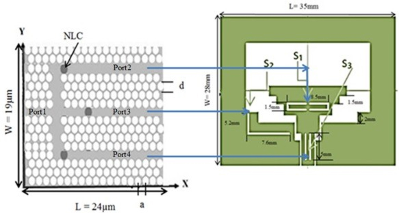
Figure 1 illustrates the designed optically controlled microstrip UWB antenna (UWBA). The proposed UWBA can work at eight modes (as shown in Table 1) using controlled switches (ON and OFF). There are three slots in the resonator; C-, L-, and U-shaped slots. The optical switches are made by placing 0.5 × 0.5 mm2 silicon wafers over the slots of the resonator. When laser is applied to all switches (ON state) the notches disappear and the antenna operates in full UWB frequency range from 2.6 to 11.8 GHz. In case, all switches are OFF, all the three notches are activated.

Fig. 1. The system of optically controlled UWB antenna using optical router.
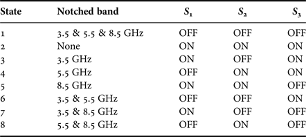
Table 1. The different states of the reconfigurable antenna.

A) Antenna design
Coplanar-fed microstrip UWB antenna was designed on a 35 × 28 mm2 FR4 substrate with relative dielectric constant of 4.6 and thickness of 1.5 mm .This design proposes triple narrow notched bands at center frequencies 3.5 GHz “WiMAX”, 5.5 GHz “WLAN” and 8.4 GHz “X-band satellite communication”. The notched bands can be achieved by adjusting the dimensions of the microstrip structure and by inserting inverted C, L, and U-shaped slots. The coplanar-fed microstrip UWB antenna is shown in Fig. 2(a), while Fig. 2(b) illustrates the inserted optically controlled switches. The proposed UWBA can work at eight modes by controlling these switches (either ON or OFF states). The optical switches are made by placing 0.5 × 0.5 mm2 silicon wafers over the slots of the resonator. When laser is applied to all switches (ON state) the notches disappear and the antenna operates in full UWB frequency range from 2.8 to 11.8 GHz. In case, all switches are OFF, all the three notches are activated. Table 1 explains the eight modes of operation of the proposed antenna. The light was directed to the switches through reconfigurable optical router with the photonic crystal substrate [Reference Areed and Obeyed10], which has one input port and three output ports.
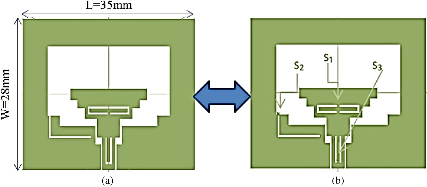
Fig. 2. The geometry of the proposed UWB antenna. (a) The original design. (b) UWB antenna without three switches.
B) Optical reconfigurable router design
The reconfigurable optical router has one input port and three output ports.
The role of the reconfigurable optical router is to direct the light to the optical switches according to the required operating state. The proposed router is composed of three photonic crystal fibers (PCFs) waveguides. Each PCF wave guide has a cavity which is filled with nematic liquid crystal (NLC) of type E7. The NLC cavities permit the optical signal to propagate through the channel by changing the external bias. According to three biasing states of each of the three NLC cavities, the router has eight operating modes. In these operating modes, the router can transmit light from one port, two ports or three ports simultaneously or no light is transmitted at all. The switches that are embedded in the antenna determine the operating mode of the UWBA. The NLCs are anisotropic materials consisting of rod-like molecules. The alignment of the NLC molecules with rotation angle φ can be controlled using two electrodes. In the unbiased state, the NLC molecules are aligned along the x-axis with rotation angle φ = 0°. However, in the biased state, the NLC molecules are oriented along the direction of the electric field in the z-direction with φ = 90° [Reference Areed and Obeyed10–Reference Areed and Obayya12]. According to the biasing state of the cavity, the light is allowed or prohibited to propagate through the switch. In the unbiased state, no light propagates (OFF state). However, in the biased state the light can propagate through the switches (ON state).
The top view of the proposed router is shown in Fig. 1. The proposed design composed of an air-hole array etched in a high-dielectric constant substrate with ε r = 11.7. Each hole has a diameter “d” of 1.2 µm. The holes are arranged in a triangular lattice structure with lattice constant “a” where d/a = 0.97. Three rows of air holes are removed from the lattice in the substrate to form a waveguide without scattering. In the front of each line, there is a hole of the same diameter “d”, which is filled with NLC of type E7.
The parameters of the supposed photonic band gap (PBG) structure are chosen in order to realize the PBG effect (zero transmission) in a certain wavelength range [Reference Areed and Obayya12–Reference Russel17].The transmission characteristics (S 21, S 31, and S 41) for this router are simulated using CST at wavelength λ = 1.55 µm and at the operating state 7 (switch S 1 is ON and switches S 2 and S 3 are OFF).The simulated values are S 21 = 0.884, S 31 = 0.045, and S 41 = 0.047. This shows that the optical power loss in ON and OFF states are 2.2 and 4.7% respectively.
C) Photonic crystal fibers
PCFs are fibers with an internal periodic structure made of capillaries, filled with air, laid to form a certain lattice structure. Light can propagate along the fiber in defects of its crystal structure. A defect is realized by removing one or more central capillaries. PCFs are anew class of optical fiber-combining properties of optical fibers and photonic crystals. They possess a series of unique properties impossible to achieve in classical fibers. The design of PCFs is very flexible. There are several parameters to manipulate: lattice pitch, air-hole shape and diameter, refractive index of the glass, and type of lattice. Freedom of design allows one to obtain endlessly single-mode fibers, which are single mode in all optical range and a cut-off wavelength does not exist. Moreover, there are two guiding mechanisms in PCF: index guiding mechanism (similar to the one in classical optical fiber) and the PBG mechanism [Reference Digge and Narayankhedkar18–Reference Broeng, Mogilevstev, Barkou and Bjarklev21]. Photonic crystal substrates for high-speed THz applications are given in [Reference Singh and Singh22].
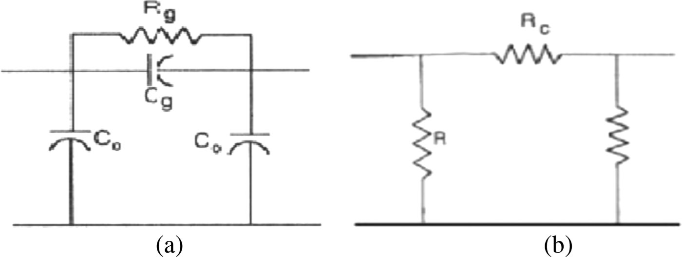
D) The optical switch
The switches are formed by placing 0.5 × 0.5 mm2 silicon wafers, having thickness t = 0.5 µm and ε r = 11.7, over the slots of the resonator. The principle of operation of such an optically controlled switch has been studied in [Reference Hindy6]. During the absence of the controlling optical signal, the model shown in Fig. 3(a) can represent the silicon wafer. The wafer conductance G g, resistance R g and capacitances C g and C o are evaluated using the equations in [Reference Hindy6]. On the other hand, when the wafer area (0.5 × 0.5 mm2) is irradiated by uniform optical power, the switch-equivalent circuit is modeled as shown in Fig. 3(b). For uniform quasi-CW irradiation, and assuming linear recombination, the dynamic wafer resistances R and R c are calculated according to formulas in [Reference Hindy6]. Incident light generates free carriers in the silicon wafer (generated photoconductivity). The switching time depends on the effective carrier lifetime, which will depend on the excess carrier concentration, and the type of recombination process takes place. In this case, the effective carrier lifetime will be in the range from 10−12 to 10−15 s, which is suitable for fast communication systems [Reference Draskovic, Panagamuwa, Vardaxoglou and Budimir5, Reference Hindy6].

Fig. 3. Equivalent circuit of the switch (a) in the absence of laser and (b) with laser.
III. SIMULATION AND EXPERIMENTAL RESULTS
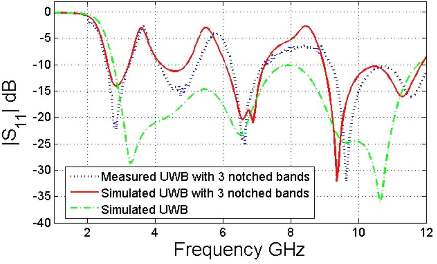
Figure 4 shows the simulated voltage standing wave ratio (VSWR) in two cases, when all switches are either OFF (state 1) or ON (state 2) as shown in Table 1. The bands with center frequencies 3.5, 5.5, and 8.5 GHz are rejected when all switches (S 1, S 2, and S 3) are OFF and consequently the UWB is divided into multiband at center frequencies 2.7, 4.7, 6.72, and 9.69 GHz. When all switches are ON, we obtain the UWB range from 2.6 to 11.8 GHz with return loss less than −10 dB and VSWR of the whole UWB is <2. Figure 5 shows the fabricated antenna, while Fig. 6 presents comparison between measured and simulated return loss (S 11). A measurement of the antenna was performed in the anechoic chamber (using VNA-Rohde&Schwarz-ZVA67) and it fits well with CST & IE3D simulations. Moreover, the average gain of this antenna is 4.5 dBi (Fig. 7).
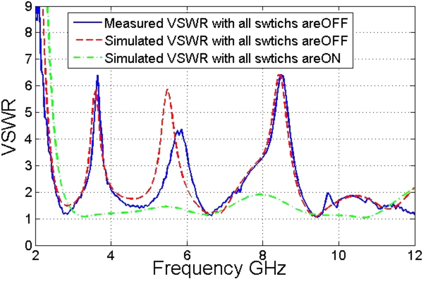
Fig. 4. VSWR of UWBA at “state1” and “state2”.

Fig. 5. Fabricated antenna.

Fig. 6. Measured and simulated S 11 for “states 1 and 2”.
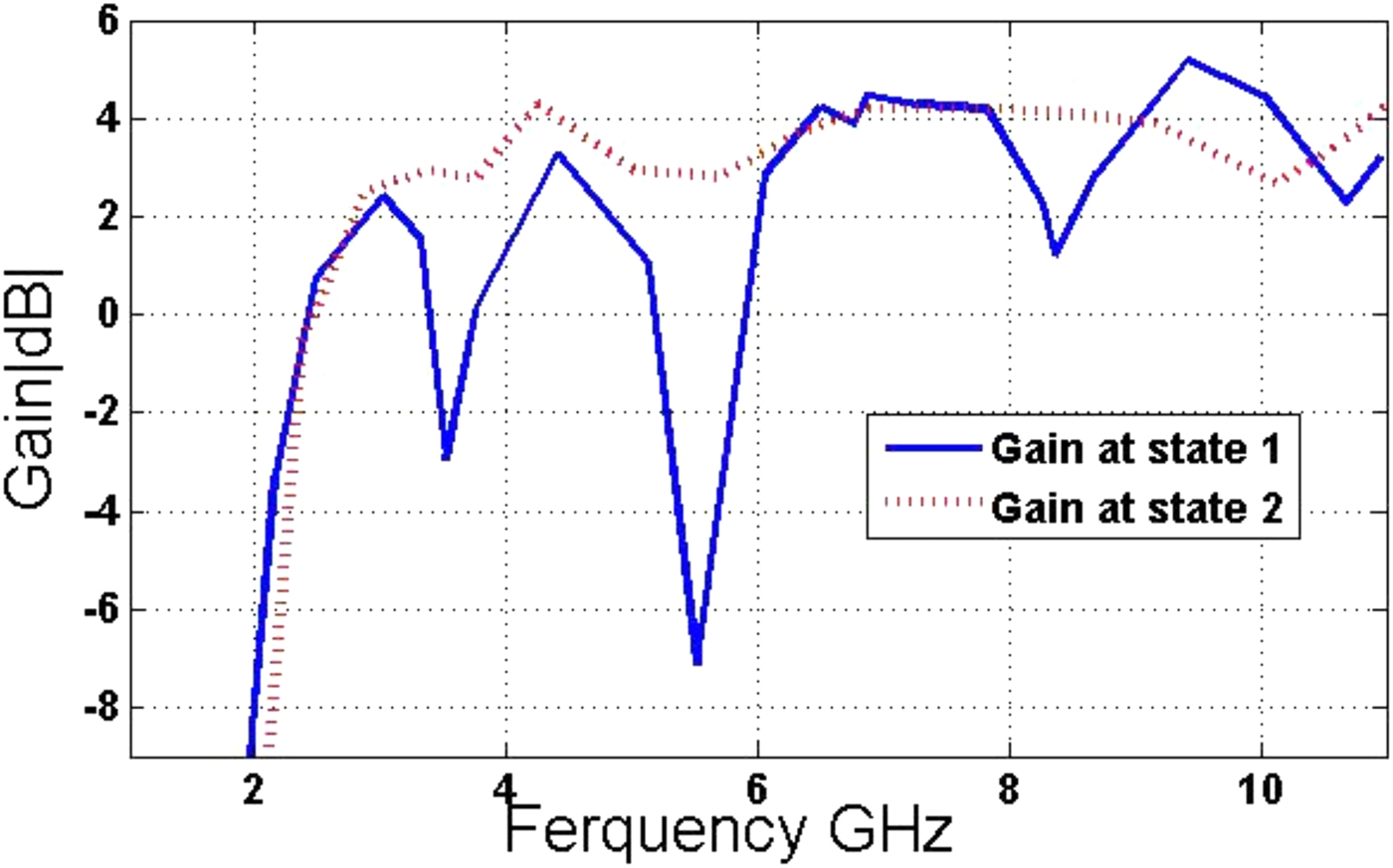
Fig. 7. UWB Antenna gain when all switches are either ON or OFF.
IV. RADIATION PATTERNS
The simulated E- and H-plane normalized radiation patterns at 3.55, 5.5, 8.425, 9.69, and 6.72 GHz for “state 1” are plotted in Fig. 8. Radiation patterns are semi-omni-directional. Three-dimensional (3D) radiation patterns are shown in Fig. 9.

Fig. 8. Radiation patterns at frequencies: (a) 3.55 GHz, (b) 5.5 GHz, (c) 8.425 GHz, (d) 9.69 GHz, and (e) 6.72 GHz.

Fig. 9. 3D Radiation patterns at frequencies 3.475, 5.455, 8.425, 9.69, and 6.72 GHz.
V. CONCLUSIONS
An optically reconfigurable notched bands UWB antenna has been presented. The antenna was designed with etched C-, L-, and U-shaped slots and integrated silicon switches. The proposed antenna has tree optical switches, which can be turned ON or OFF according to the incident light. The incident light is coupled to the switches through an optical router. The reconfigurable optical router has three PCF waveguides with a NLC cavity at the entrance of each one. The router directs the light to the optical switches by changing the external bias of the NLC cavities. The proposed antenna yields an UWB that extends from 2.6 to 11.8 GHz with switchable single notched bands of 3.5, 4.5, or 8.5 GHz for WiMAX, WLAN, and other applications .The measured results of the proposed antenna well agree with the simulated ones. The antenna radiation patterns are almost omni-directional in the pass band ranges with quite satisfactory gain. This proposed design can work on eight modes, which are suitable for multimode, multiband, and UWB radio communications.
 Engineer Heba Z. Afify received the M.Sc. degree from Ain-Shams University, Faculty of Engineering on May 2016 and B.Sc. from Thebes-Academy, Cairo, Egypt, on May 2011. Her area of research is Microwave Engineering and Optical Control.
 Professor Moataza Hindy works at the Electronic Research Institute. She has been a full Professor since 1999 and was an Associate Professor and Researcher in 1989 and 1984, respectively. She received her Ph.D. degree from Moscow University in 1983 in the area of microwaves and optoelectronics, M.Sc. in Electronics and Communications from the Faculty of Engineering Ain-Shams University in 1977. Professor Hindy graduated from the electronics and communications department of the Faculty of Engineering Cairo University in 1972. Her areas of research are Microwaves and Electromagnetics, Optoelectronics, Optical communications, and Optical Control of Microwave Devices. She has published over 95 research papers, and has worked as a reviewer and examiner for M.Sc. and Ph.D. thesis in many universities in Egypt. Professor Hindy has supervised more than 40 graduate thesis/dissertations and worked as ex-Chairman of “Micro strip Department” in Electronics Research Institute, Cairo, Egypt. She has contributed as a speaker in many international conferences. She shared in the development of the courses and programs for communication and electronic engineers (M.Sc. and B.Sc. programs) in the University of Bahrain.
 Adel El Henawy was a Full professor in the Department of Communications and Electronics, Faculty of Engineering, Ain-Shams University. He passed away a few months ago.