


I. INTRODUCTION
As the Federal Communication Commission (FCC) allocated 3.1–10.6 GHz for ultra-wide band (UWB) applications in 2002 [1], an era of high-speed and short-distance communication was coming. However, the bandwidth of the UWB system covers about 7 GHz, and there are many other communication systems in this frequency range. Therefore, UWB antennas with band-notched characteristics are required to filter out interference signals generated by other coexisting communication systems. A lot of UWB antennas, which are designed with different band-notched properties, have been reported in recent research papers [Reference Zhang, Hong, Yu, Kuai, Don and Zhou2–Reference Hong, Ling, Tarn and Chung10].
In [Reference Zhang, Hong, Yu, Kuai, Don and Zhou2], a technique with multiple etched slots on the patch and split ring resonators (SRR) coupled to feed line was proposed to obtain an UWB antenna with triple notch bands. An UWB antenna realized triple notch bands by embedding an Omega-shaped slot on the radiating patch in [Reference Li, Shi and Hei3]. A compact triple notch bands UWB antenna with complementary co-directional split-ring resonator (CSRR) arranged in the middle of the radiating patch close to the feeding strip was presented in [Reference Tang4]. Similarly, dual notch bands UWB antenna with modified complementary CSRR etched on the patch was fabricated in [Reference Li, Zhou, Hong, Wang and Sun5]. Some other UWB antennas realized dual notch bands by using quasi-complementary SRR in [Reference Li, Hei, Feng and Shi6], and by using two nested C-shaped slots in [Reference Chu and Yang7]. Moreover, single notch band UWB antenna realized by stub-loaded SRR was proposed in [Reference Siddiqui, Saha and Antar8]. In [Reference Peng and Ruan9], an UWB antenna was configured by utilizing a mushroom-type electromagnetic-bandgap structure to achieve single notch band. Another single notch band UWB antenna consisting of a patch with arc-shaped edge and a partially modified ground plane was presented in [Reference Hong, Ling, Tarn and Chung10].
All the antennas mentioned above can achieve their band-notch characteristics as expected. Nevertheless, some techniques they adopted are complicated, which may be unsuitable to be applied in low-cost UWB antenna applications. Furthermore, in some single notch band UWB antennas, the notch bands are not wide enough, so they cannot reject unwanted signals in a wide range. The notch band of the UWB antenna in [Reference Siddiqui, Saha and Antar8] nearly ranges from 6.21 to 6.57 GHz, and the notch bandwidth is 0.36 GHz. In [Reference Peng and Ruan9], the notch band has a bandwidth of 0.69 GHz and ranges from 5.62 to 6.31 GHz. The antenna in [Reference Hong, Ling, Tarn and Chung10] has a rejection frequency band of 5.11 to 5.98 GHz (notch bandwidth is 0.87 GHz). In fact, most of the unwanted narrow band signals from other communication systems are actually scattered in a wide range, then an UWB antenna with wide band-notched characteristics is required. Hence, inspired by the SRR structure in [Reference Sanz, Belenguer, Martinez, Borja, Cascon and Boria11], this paper presents a novel coplanar waveguide (CPW) fed UWB antenna with modified SRR to get wide band-notched characteristics. A circular patch with CPW is fabricated on the front surface of the antenna, and the SRR connected by open-ended microstrip lines are fabricated on the back side. This UWB antenna operates from 2.37 to 10.93 GHz, and the notch band is ranging from 4.96 to 6.15 GHz with bandwidth of 1.19 GHz. The relative stopped bandwidth (RSB) of the notch band is 20.42%, and all the frequency bands of the IEEE 802.11.ac are covered in this notch band of the proposed UWB antenna.
II. ANTENNA DESIGN CONSIDERATION
Figure 1(a) shows the structure of a traditional UWB antenna using a circular patch fed by CPW. A modified structure of an UWB antenna, which incorporates etched stubs and loaded SRR in the middle of the CPW, is illustrated in Fig. 1(b). The structure of the UWB antenna proposed in this paper is charted in Fig. 1(c); a pair of microstrip lines is added and connected to the SRR in this work. Figure 2 displays the enlarged view of the SRR and the microstrip line.

Fig. 1. Schematics of different UWB antennas.

Fig. 2. The enlarged view of the SRR and the microstrip line.
The fabricated prototype of the proposed UWB antenna is demonstrated in Fig. 3. On the top side of this UWB antenna in Fig. 3(a), the circular monopole has a radius R of 12.5 mm and is fed with the CPW having ground plane area of W 3 × L 2, the width W 3 is 50 mm and the length L 2 is 22.4 mm. As a result of the current distributes along the ground plane width and the ground plane acts as an impedance matching circuit, the antenna performance is vitally influenced by the ground plane [Reference Liang, Guo, Chiau, Chen and Parini12]. A pair of SRR connected by microstrip lines is printed on the back side of the antenna, which is illustrated in Fig. 3(b). When the EM signal spreads along the CPW, it induces an electromotive force on the SRR, and then induces current oscillating between the two rings of the SRR. These oscillating currents between the two rings generate a resonance, which blocks signal propagation at a specific frequency. The calculation of the specific resonance frequency will be discussed in later section. All parameters of the proposed UWB antenna have been listed in Table 1. This proposed UWB antenna was fabricated on a Taconic substrate with h = 1.575 mm, dielectric constant ε r of 2.33 and a loss tangent of 0.0009 to verify its performance.

Fig. 3. Fabricated prototype of the proposed UWB antenna.
Table 1. Design parameters of the proposed antenna.
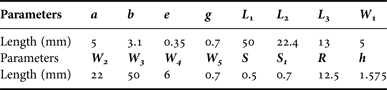
Figure 4 shows the simulated return losses of the traditional, the modified and the proposed UWB antennas. From the simulated results, the traditional UWB antenna has two transmission poles in the UWB frequency, and the modified UWB antenna with band-notched characteristics has three poles. Contrastively, the proposed UWB antenna possesses four poles, and the band-notched behavior is obtained from 4.95 to 6.15 GHz (|S 11| is bigger than −10 dB). Moreover, the notch band of this proposed UWB antenna has two transmission zeros (f 1 and f 2).

Fig. 4. The simulated return losses of the traditional, modified and proposed UWB antennas.
III. RESONANCE FREQUENCY ANALYSIS
According to [Reference Marques, Martin and Sorolla13], the resonance frequency f 1 of the SRR is given as:
 $$f_1 = \displaystyle{1 \over {2\pi}} \sqrt {\displaystyle{1 \over {L_rC_r}}}, $$
where the C r is the total equivalent capacitance of the SRR and can be evaluated as:
 $$C_r = \left( {2a_{avg} - \displaystyle{g \over 2}} \right)C_{pul} + \displaystyle{{\varepsilon _0et_m} \over {2g}},$$
where the e and t m are the width and thickness of the metallic rings, respectively. The ε 0 is the free space permittivity and the average ring dimension a avg can be calculated as:
 $$a_{avg} = \displaystyle{a \over 2} - e - \displaystyle{{a - b} \over 4}.$$
The capacitance of C pul is analyzed in [Reference Bahl and Bhartia14] and it can be given as follow:
 $$C_{pul} = \displaystyle{{\sqrt {\varepsilon _e}} \over {c_0Z_0}},$$
where c 0 = 3 × 10⁸ m/s and Z 0 is the intrinsic impedance of the transmission line. The ε e is the effective permittivity of the medium and can be expressed as:
 $$\varepsilon_e = \displaystyle{{\varepsilon _r + 1} \over 2}.$$
Based on the analysis in [Reference Terman15], the total equivalent inductance L r of the SRR can be evaluated as:
 $$L_r = 0.0002l\left( {2.303{\log} _{10}\displaystyle{{4l} \over e} - \gamma} \right),$$
where the constant γ = 2.853 and the wire length l = 4a–g. Thus, the resonance frequency f 1 of the SRR can be evaluated by using (1)–(6). Moreover, as charted in Fig. 1(c), a pair of microstrip lines connecting to the SRR is designed in this work. Hence, equations (7)–(9) are used to evaluate the resonance frequency f 2 of the microstrip lines:
 $$f_2 = \displaystyle{{c_0} \over {2 \times W_5}}\sqrt {\displaystyle{2 \over {\varepsilon _r + 1}}}, $$
 $$f_2 = \displaystyle{1 \over {(L_3 + 2\Delta L)\sqrt {\varepsilon _e} \sqrt {\varepsilon _0\mu _0}}}, $$
 $$\Delta L = 0.412\displaystyle{{(\varepsilon _e + 0.3)((W_5/h) + 0.264)} \over {(\varepsilon _e - 0.258)((W_5/h) + 0.8)}},$$
where L 3 is the length of microstrip line, and W 5 is the width of it. It is apparent that the f 2 is separately affected by W 5 in (7) and dominated by L 3 in (8). Simulated results for testifying the influence of W 5 and L 3 on f 2 will be demonstrated in Section IV.
IV. RESULTS AND DISCUSSIONS
As two different equations of f 2 have been discussed in Section III, different values of W 5 and L 3 are utilized in simulation to testify their effect on f 2. Figure 5 shows the simulated return losses of the proposed UWB antenna for different L 3. It can be figured out from the curves that the resonance frequency f 2 is decreasing as the length of microstrip line L 3 increases, while the resonance frequency f 1 is nearly unchanged. Meanwhile, the bandwidth of the notch band is increasing along with the increasement of L 3. However, the L 3 cannot be lengthened immoderately, as the whole operating frequency of the antenna will be reduced and fails to cover the UWB bandwidth from 3.1 to 10.6 GHz when L 3 increases. Therefore, the L 3 = 12 mm is selected as the optimized length in this proposed UWB antenna.

Fig. 5. Simulated return losses versus frequency of the proposed UWB antenna for different L 3.
The simulated return losses of the proposed UWB antenna for different W 5 are drawn in Fig. 6. It is denoted in Fig. 6 that the resonance frequency f 1 and f 2 are scarcely changed when the W 5 increases, while the cut-off frequency of the proposed UWB antenna is varied. In accordance with these issues, the width of 0.7 mm is adopted as the optimal option.

Fig. 6. Simulated return losses versus frequency of the proposed UWB antenna for different W 5.
In Fig. 7, the simulated and measured return losses versus frequency of the proposed UWB antenna are presented. It is easy to find out that the simulated and measured results are coincided. The proposed UWB antenna operates in the 2.37–10.93 GHz frequency range with notch band from 4.96 to 6.15 GHz, and the RSB of notch band is about 20.42%. The resonance frequency f 1 of SRR is 5.12 GHz and the resonance frequency f 2 of microstrip line is 5.96 GHz, respectively. Figure 8 draws the simulated and measured gain versus frequency of the proposed UWB antenna. At the notch band of 4.96 to 6.15 GHz, the gain reduces sharply (<0 dBi), whereas the gain for the rest of the operating frequency remains acceptable. The return losses and gain performances of the proposed UWB antenna well validate the theoretical analysis in Section III, and indicate that this antenna can efficiently reject unwanted interference signals in the notch band frequency.

Fig. 7. Simulated and measured return losses versus frequency of the proposed UWB antenna.

Fig. 8. Simulated (solid line) and measured (dotted line) gain versus frequency of the proposed UWB antenna.
Figure 9 shows the measured group delay versus frequency of the proposed UWB antenna. As it can be seen from Fig. 9, the variation of the group delay is relatively stable for the operating frequency, while the variation of the group delay is bigger than 0.5 ns for the notch band. Figure 10 illustrates measured radiation patterns of the E- and H-planes at three different sample frequencies of 3.0, 7.2, and 10.0 GHz. From Fig. 10, it is obvious that the proposed antenna has acceptable omnidirectional radiation patterns at all three specific frequencies, which indicates that signals can be transmitted efficiently by this UWB antenna in the non-notched band. The group delay and radiation patterns performances denote that the proposed UWB antenna is suitable to be applied in most UWB wireless communication systems requiring band-notch characteristics.

Fig. 9. Measured group delay versus frequency of the proposed UWB antenna.

Fig. 10. Measured co-polarization (solid line) and cross-polarization (dotted line) radiation patterns of E- and H-planes of the proposed UWB antenna at different frequencies: (a) 3.0 GHz, (b) 7.2 GHz, and (c) 10.0 GHz.
The performance comparisons of the proposed antenna with other reported antennas are summarized in Table 2. It is clear that the notch band of the proposed UWB antenna ranges wider than other antennas with larger notch bandwidth of 1.19 GHz. The higher RSB percentage shows that the proposed UWB antenna has wider band-notched characteristics.
Table 2. Comparison of this work with other UWB antennas.

V. CONCLUSION
This paper presents a novel SRR-loaded CPW-fed antenna with wide band-notched characteristics for UWB applications. Some designing parameters are optimized by CST and HFSS software. The proposed antenna operates in the range from 2.37 to 10.93 GHz with a wide notch band frequency from 4.96 to 6.15 GHz, and the RSB of notch band is up to 20.42%. Theoretical analysis and experimental results both indicate that this proposed UWB antenna can be utilized in many UWB applications.
ACKNOWLEDGEMENTS
The authors thank the editors and anonymous reviewers for their valuable comments which helped in improving this manuscript. The authors also thank Dr. David and Dr. Hu for the English improvements of this paper. This research was supported by the National Natural Science Foundation of China (Grants No. 61274020, 61571185 and 61561022) and the Open Fund Project of Key Laboratory in Hunan Universities (Grant No. 15K027).
 Haijun Peng was born in 1991 in Yongzhou, China. He received the B.S. degree in the major of Information and Communication Engineering from Hunan Institute of Science and Technology, Yueyang, China and his post-graduation is in the field of integrated circuit from the College of Information Science and Engineering, Hunan University, Changsha, China. His research interests are mainly in wireless communication circuit, ultra-low power, and UWB RFIC design.
 Chunhua Wang was born in Yongzhou, China, in 1963. He received the B.S. degree from Hengyang Normal College, Hengyang, China, in 1983; the M.S. degree from Physics Department, Zheng Zhou University, Zheng Zhou, China, in 1994; and the Ph.D. degree from the School of Electronic Information and Control Engineering, Beijing University of Technology, Beijing, China, in 2003. He is currently a Professor of College of Information Science and Engineering, Hunan University, Changsha, China. His research interests include current-mode circuit design, filtering, radio frequency circuit, and wireless communications.
 Lv Zhao was born in Xiangtan, China, in 1986. He received the B.S. degree from Hunan University of Science and Technology, Xiangtan, China, in 2008; and the M.S. degree from College of Information Science and Engineering in Guangxi University, in 2012. He is currently studying in Hunan University for the Ph.D. degree. His research interests are focused on RF front-end circuits design and wireless communications.
 Jun Liu was born in 1974, received his Ph.D., and was the Professor of Engineering. Currently, he is an engineer at the STATE GRID HUNAN Electric Power Company. His main research interests include optical communications, wireless communications, next-generation networking, and Internet.


